RECENT ADVANCES IN DISPLAY TECHNOLOGIES RAMACHANDRA RAO DASARI

- Slides: 43

RECENT ADVANCES IN DISPLAY TECHNOLOGIES RAMACHANDRA RAO DASARI DISTINGUISHED LECTURE SERIES ON LASER TECHNOLOGY, LASER SPECTROSCOPY & OPTOELECTRONICS Dr. K. R. Sarma Adviser Technology Samtel Group

ATTRIBUTES HIGH RESOLUTION HIGH BRIGHTNESS LARGE VIEWING ANGLE HIGH WRITING SPEEDS LARGE COLOUR GAMUT HIGH CONTRAST LESS WEIGHT AND SIZE LOW POWER CONSUMPTION LOW COST

TECHNOLOGIES CATHODE RAY TUBE (CRT) VACUUM FLOURECENT DISPLAY (VFD) FIELD EMISSION DISPLAY (FED) LIQUID CRYSTAL DISPLAY (LCD) PLASMA DISPLAY PANEL (PDP) ELECTROLUMINISCENT DISPLAY (EL) ORGANIC LIGHT EMITTING DIODE (OLED)

CRT 100 YEAR OLD WORKHORSE CATHODOLUMINISCENT BEAM SCAN DEVICE LARGE VIEWING ANGLE HIGH BRIGHTNESS HIGH RESOLUTION GOOD COLOUR GAMUT BEST PERFORMANCE TO COST BULKY HEAVY UNIMPLEMENTABLE IN LARGE SIZES OBSOLESCENCE STILL ENJOYS 70% MARKET

VFD Earliest Flat technology Low Cost Good Luminance Excellent Viewing Angle Long Life Matrix Addressing Wire Emitters Cathodoluminescent Mechanical Complexity Low Resolution High Filament Power

FED MATRIX DISPLAY LARGE VIEWING ANGLE HIGH BRIGHTNESS, HIGH RESOLUTION EXCELLENT COLOUR GAMUT TECHNOLOGY NOT MATURE

FIELD EMISSION SPINDT STRUCTURE MIM SURFACE EMISSION CARBON DIAMOND LIKE FILMS CARBON NANOTUBES

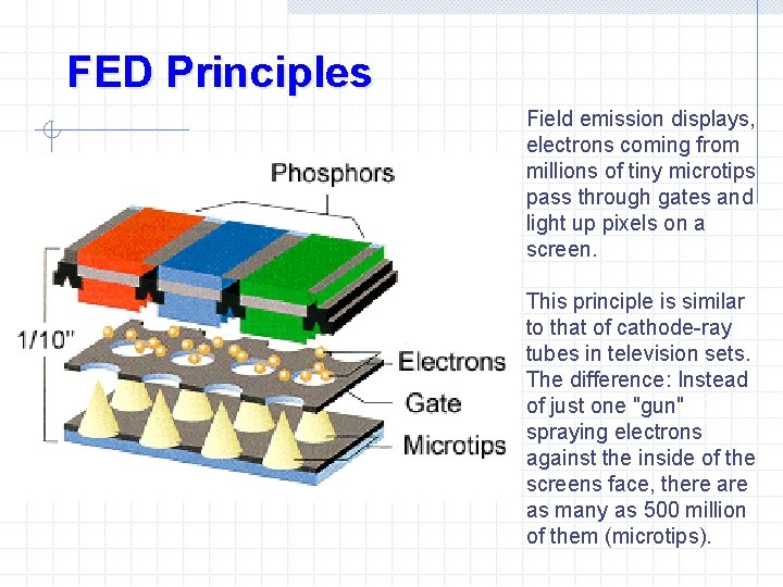
FED Principles Field emission displays, electrons coming from millions of tiny microtips pass through gates and light up pixels on a screen. This principle is similar to that of cathode-ray tubes in television sets. The difference: Instead of just one "gun" spraying electrons against the inside of the screens face, there as many as 500 million of them (microtips).

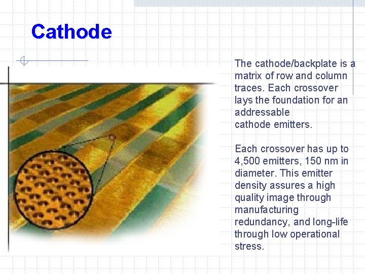
Cathode The cathode/backplate is a matrix of row and column traces. Each crossover lays the foundation for an addressable cathode emitters. Each crossover has up to 4, 500 emitters, 150 nm in diameter. This emitter density assures a high quality image through manufacturing redundancy, and long-life through low operational stress.

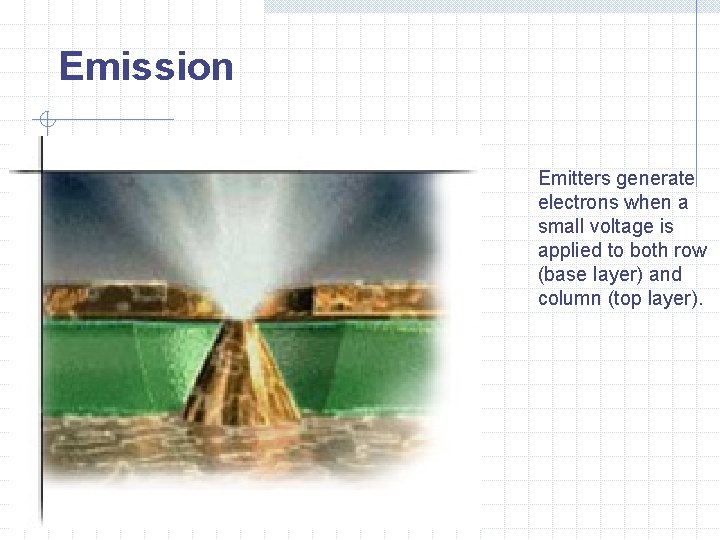
Emission Emitters generate electrons when a small voltage is applied to both row (base layer) and column (top layer).

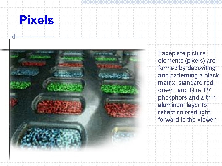
Pixels Faceplate picture elements (pixels) are formed by depositing and patterning a black matrix, standard red, green, and blue TV phosphors and a thin aluminum layer to reflect colored light forward to the viewer.

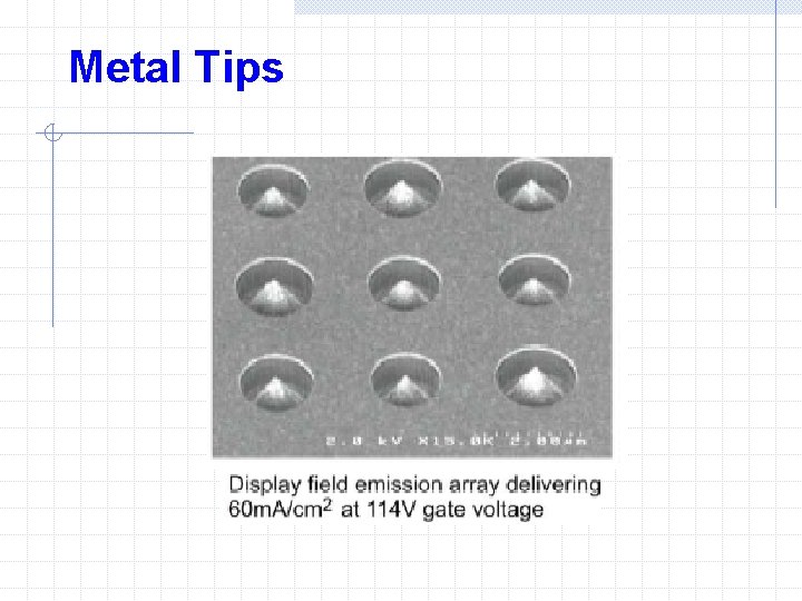
Metal Tips

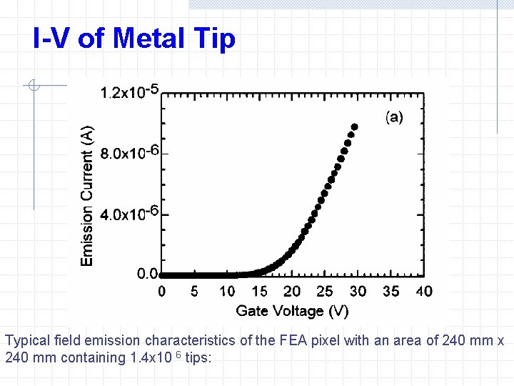
I-V of Metal Tip Typical field emission characteristics of the FEA pixel with an area of 240 mm x 240 mm containing 1. 4 x 10 6 tips:

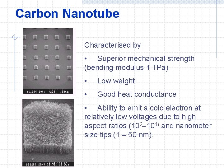
Carbon Nanotube Characterised by • Superior mechanical strength (bending modulus 1 TPa) • Low weight • Good heat conductance • Ability to emit a cold electron at relatively low voltages due to high aspect ratios (102– 104) and nanometer size tips (1 – 50 nm).

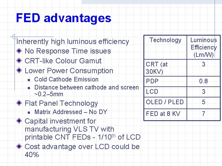
FED advantages Inherently high luminous efficiency No Response Time issues CRT-like Colour Gamut Lower Power Consumption n n Cold Cathode Emission Distance between cathode and screen ~0. 2– 5 mm Flat Panel Technology n Matrix Addressed – No DY Capital investment for manufacturing VLS TV with printable CNT FEDs - 1/10 th of LCD Cost advantage over LCD could be 40% Technology CRT (at 30 KV) Luminous Efficiency (Lm/W) 3 PDP 0. 8 LCD 3 OLED / PLED 5 FED at 8 KV 7

FED Technology Roadblocks Spindt type FED n n n Yield problems – Tip wear off, high vacuum High cost of submicron technology for Spindt type emitters High Voltage Breakdown due to electron bombardment and spacer charging Phosphor decay in case anode is at low voltage to counter the above problem Backscatter from anodes at high anode voltages leading to cross talk

FED – Technology Options Spindt Type Emitters n Oldest, Expensive and Yield problems Carbon Nanotube Emitters (Max R&D funds) n n n Japanese funding lot of research for display application Has problems with Short range uniformity Potential of low cost printing for manufacture SED (Surface-Conduction Electron-Emitter Display) n n Does not have emitting tips, uses electron tunneling Being pursued by Toshiba – Canon (IPR bought from Candescent) for commercialisation (50” prototype by 2005)

EL The structure consists of two thin layers of dielectric with phosphor sandwitched between them. A thin Al layer on the top and thin ITO layer on the bottom completes EL. When voltage of order of 200 V is applied the resultant high electric field (1 MV/cm) tunnels electrons through dielectric on to phosphor. The high energy of electrons impact the colour centres to emit visible light. High brightness, high resolution, Blue phosphor improvement required High voltage switching High purity materials Small sizes Expensive

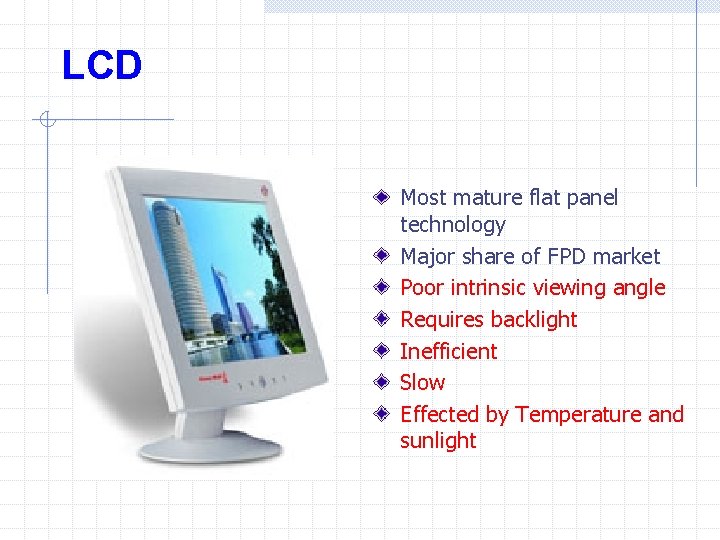
LCD Most mature flat panel technology Major share of FPD market Poor intrinsic viewing angle Requires backlight Inefficient Slow Effected by Temperature and sunlight

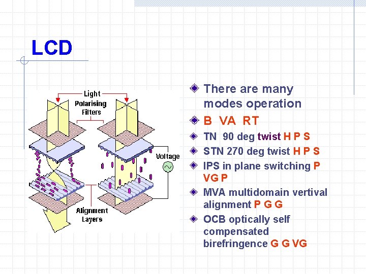
LCD There are many modes operation B VA RT TN 90 deg twist H P S STN 270 deg twist H P S IPS in plane switching P VG P MVA multidomain vertival alignment P G G OCB optically self compensated birefringence G G VG

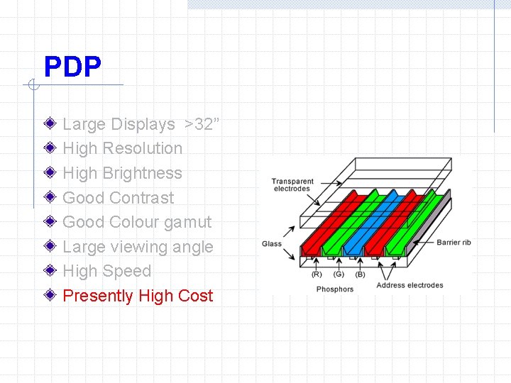
PDP Large Displays >32” High Resolution High Brightness Good Contrast Good Colour gamut Large viewing angle High Speed Presently High Cost

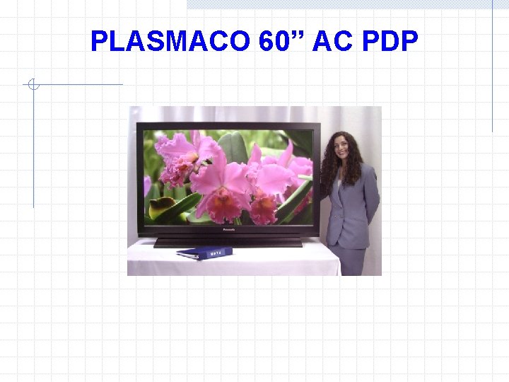
PLASMACO 60” AC PDP

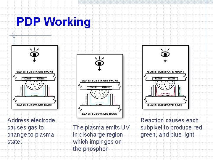
PDP Working Address electrode causes gas to change to plasma state. The plasma emits UV in discharge region which impinges on the phosphor Reaction causes each subpixel to produce red, green, and blue light.

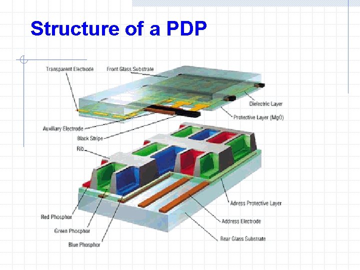
Structure of a PDP

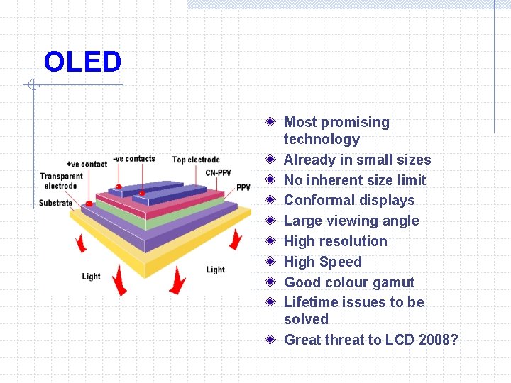
OLED Most promising technology Already in small sizes No inherent size limit Conformal displays Large viewing angle High resolution High Speed Good colour gamut Lifetime issues to be solved Great threat to LCD 2008?

OLED advantages Colour Gamut comparable to CRT, with potential to get better – Striking visual appeal Thinner – No backlight Less Expensive than LCD due to lesser components n White + Color Filter route takes away some of this advantage Potential for printing in manufacturing. Flexible and Conformal Displays

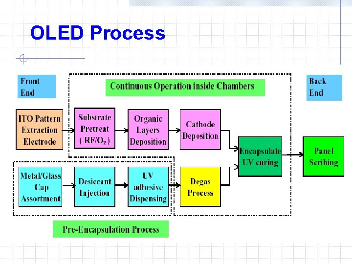
OLED Process

OLED Roadblocks Materials n Small molecule lifetimes still not OK for TV applications, although robust for mobile phones n Polymers struggling with material stability Manufacturing n UHV process not easily scalable to larger Mother Glass. Currently, manufacturing restricted to 370 x 470 mm n Printing (Polymers) still in R&D stage Active Matrix Back plane n Incompatible with the existing a: Si technology n LTPS technology (considered suitable for current driven devices) suffers from uniformity problems and restricted to displays < 8”


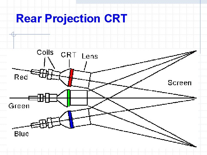
Rear Projection CRT

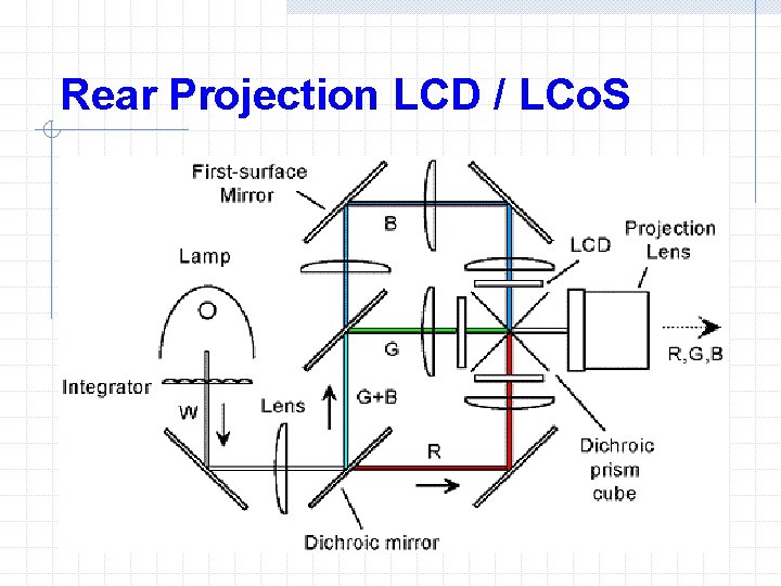
Rear Projection LCD / LCo. S

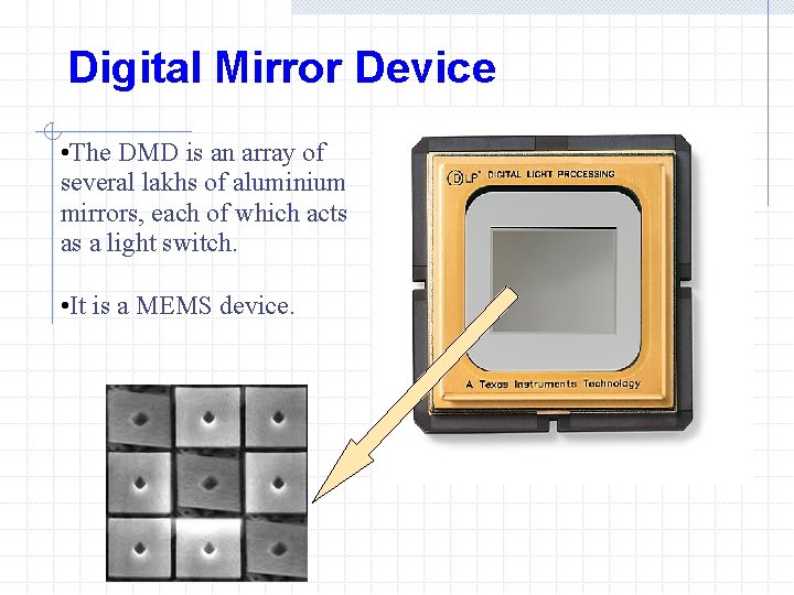
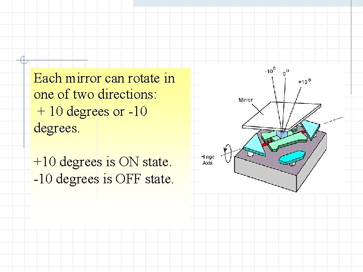
Digital Mirror Device • The DMD is an array of several lakhs of aluminium mirrors, each of which acts as a light switch. • It is a MEMS device.

Each mirror can rotate in one of two directions: + 10 degrees or -10 degrees. +10 degrees is ON state. -10 degrees is OFF state.

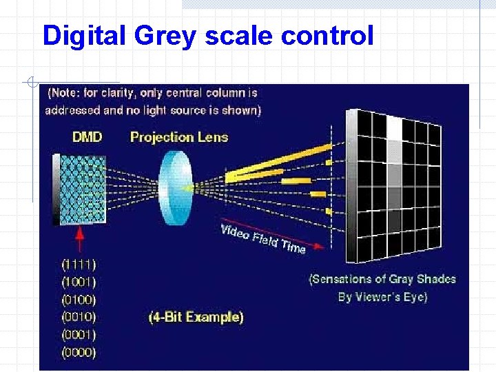
Digital Grey scale control

Grating Light Valve Originally developed and patented by Professor David Bloom and his students at Stanford University. Further work done by Silicon Light Machines. GLV technology acquired by SONY for applications in display devices => Expect rapid growth. In the high-end display market (simulation, planetarium) Silicon Light Machines is partnered with Evans & Sutherland. Silicon Light Machines acquired by Cypress Semiconductor Corporation - GLV technology for optical communication.

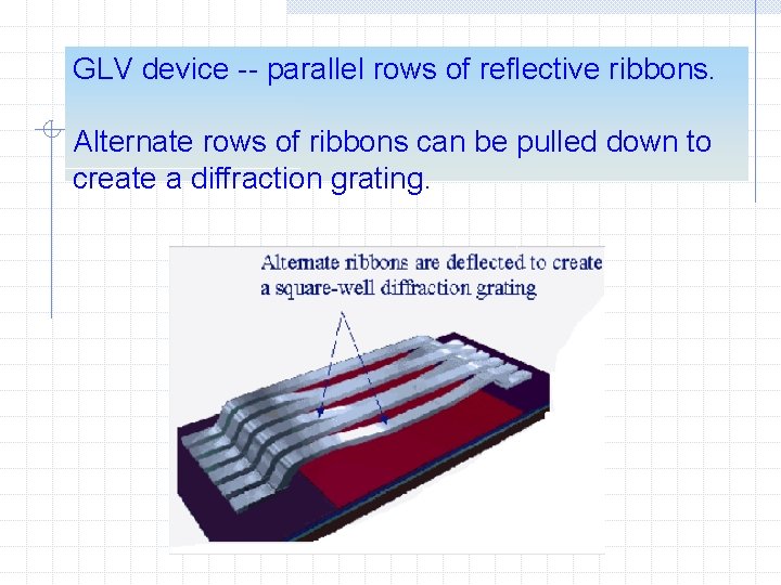
GLV device -- parallel rows of reflective ribbons. Alternate rows of ribbons can be pulled down to create a diffraction grating.

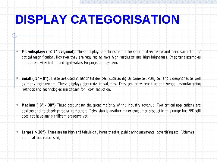
DISPLAY CATEGORISATION

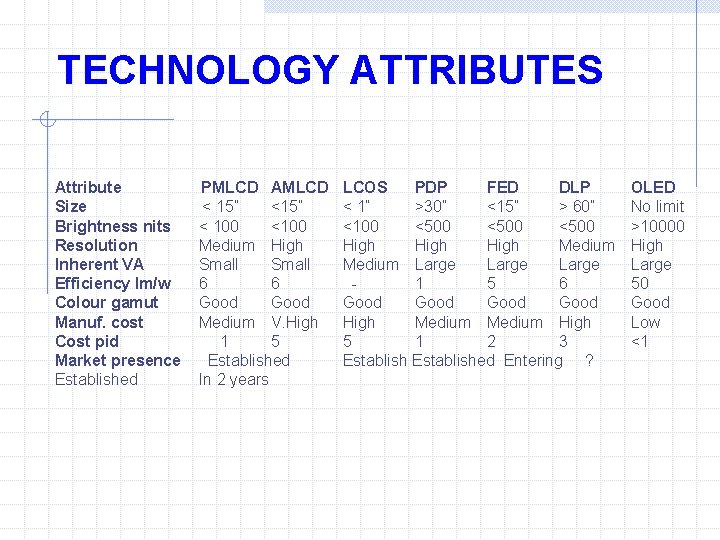
TECHNOLOGY ATTRIBUTES Attribute Size Brightness nits Resolution Inherent VA Efficiency lm/w Colour gamut Manuf. cost Cost pid Market presence Established PMLCD AMLCD < 15” < 100 <100 Medium High Small 6 6 Good Medium V. High 1 5 Established In 2 years LCOS PDP FED DLP < 1” >30” <15” > 60” <100 <500 High Medium Large 1 5 6 Good High Medium High 5 1 2 3 Established Entering ? OLED No limit >10000 High Large 50 Good Low <1

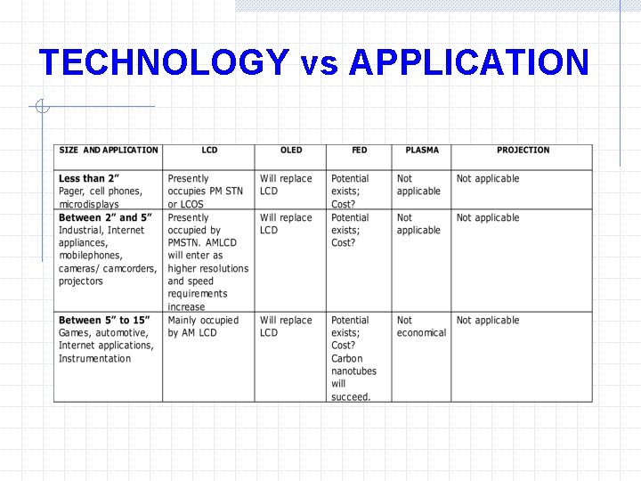
TECHNOLOGY vs APPLICATION

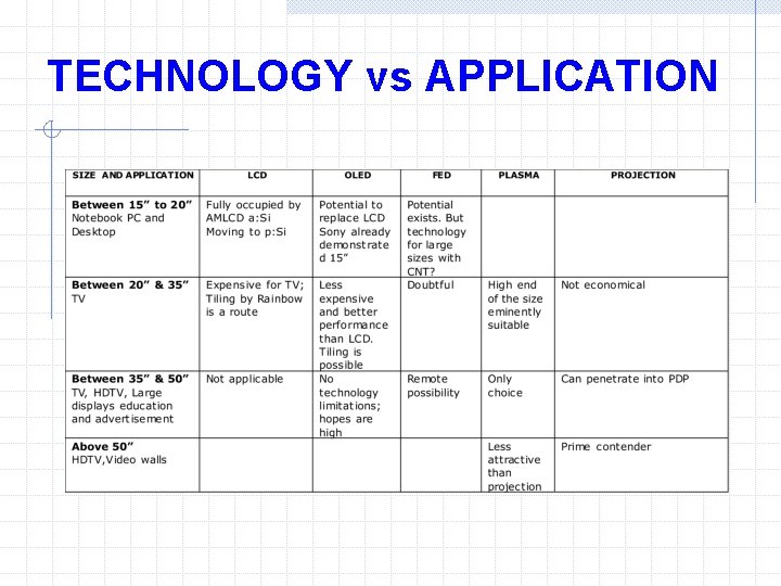
TECHNOLOGY vs APPLICATION

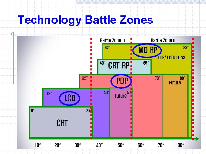
Technology Battle Zones

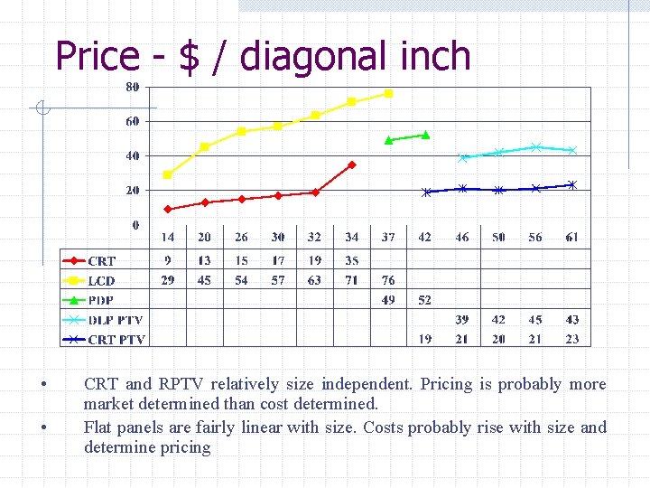
Price - $ / diagonal inch • • CRT and RPTV relatively size independent. Pricing is probably more market determined than cost determined. Flat panels are fairly linear with size. Costs probably rise with size and determine pricing

Thank you