Readout System of the CMS Pixel Detector JC

- Slides: 1

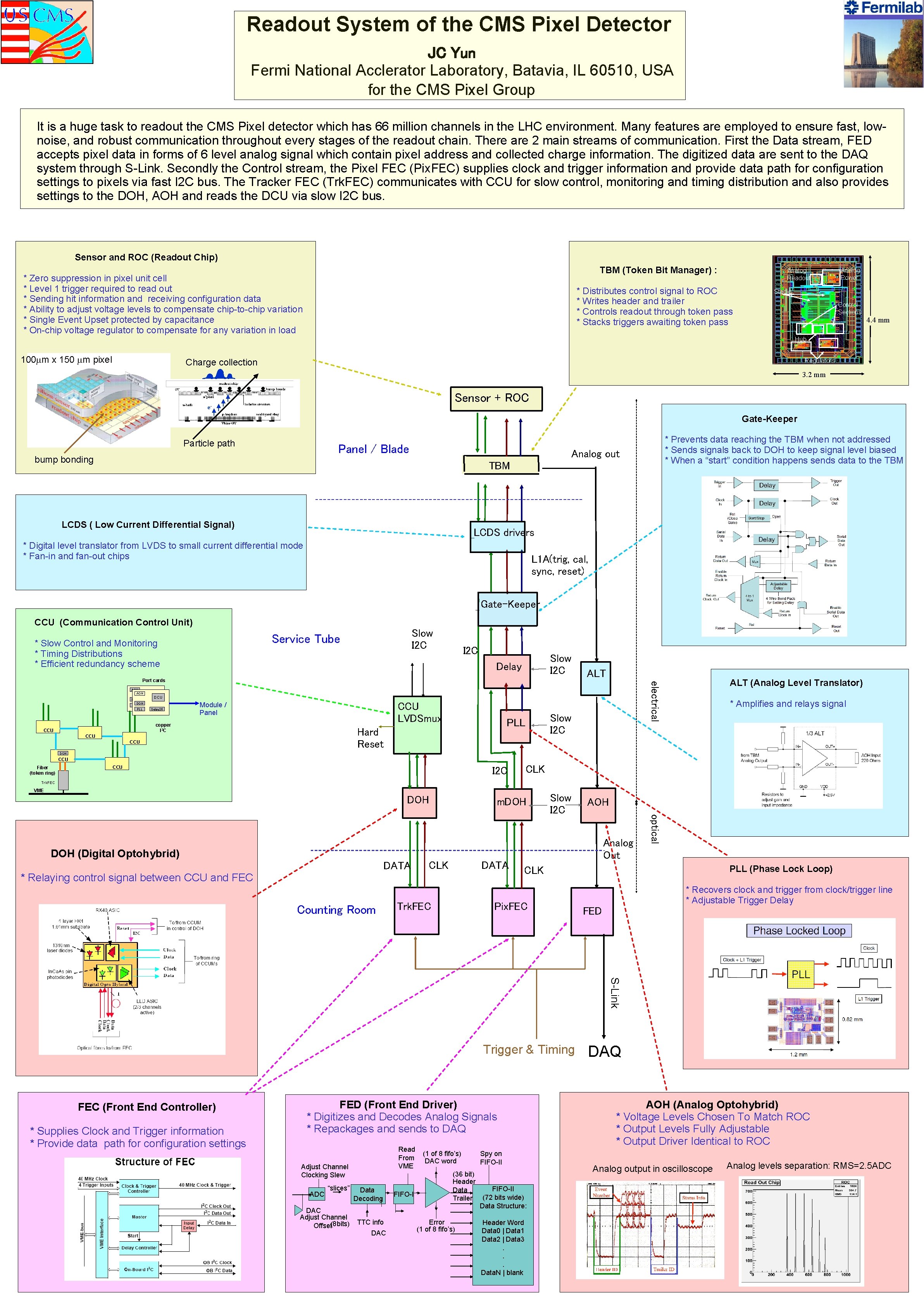
Readout System of the CMS Pixel Detector JC Yun Fermi National Acclerator Laboratory, Batavia, IL 60510, USA for the CMS Pixel Group J. C. Youth It is a huge task to readout the CMS Pixel detector which has 66 million channels in the LHC environment. Many features are employed to ensure fast, lownoise, and robust communication throughout every stages of the readout chain. There are 2 main streams of communication. First the Data stream, FED accepts pixel data in forms of 6 level analog signal which contain pixel address and collected charge information. The digitized data are sent to the DAQ system through S-Link. Secondly the Control stream, the Pixel FEC (Pix. FEC) supplies clock and trigger information and provide data path for configuration settings to pixels via fast I 2 C bus. The Tracker FEC (Trk. FEC) communicates with CCU for slow control, monitoring and timing distribution and also provides settings to the DOH, AOH and reads the DCU via slow I 2 C bus. Sensor and ROC (Readout Chip) TBM (Token Bit Manager) : * Zero suppression in pixel unit cell * Level 1 trigger required to read out * Sending hit information and receiving configuration data * Ability to adjust voltage levels to compensate chip-to-chip variation * Single Event Upset protected by capacitance * On-chip voltage regulator to compensate for any variation in load Analog Readout * Distributes control signal to ROC * Writes header and trailer * Controls readout through token pass * Stacks triggers awaiting token pass Analog Power Stacks Control Sections 4. 4 mm Hub 100 m x 150 m pixel Charge collection Regulators 3. 2 mm Sensor + ROC e- Gate-Keeper Particle path Panel / Blade bump bonding * Prevents data reaching the TBM when not addressed * Sends signals back to DOH to keep signal level biased * When a “start” condition happens sends data to the TBM Analog out TBM LCDS ( Low Current Differential Signal) LCDS drivers * Digital level translator from LVDS to small current differential mode * Fan-in and fan-out chips L 1 A(trig, cal, sync, reset) Gate-Keeper CCU (Communication Control Unit) Slow I 2 C Service Tube * Slow Control and Monitoring * Timing Distributions * Efficient redundancy scheme I 2 C Slow I 2 C Delay AOH DCU DOH PLL Delay 25 CCU LVDSmux Module / Panel copper I 2 C CCU Hard Reset CCU Slow I 2 C PLL ALT (Analog Level Translator) electrical Port cards ALT * Amplifies and relays signal DOH CCU Fiber (token ring) CCU CLK I 2 C Trk. FEC VME DOH m. DOH Analog Out DOH (Digital Optohybrid) DATA CLK DATA * Relaying control signal between CCU and FEC Counting Room Trk. FEC optical Slow I 2 C PLL (Phase Lock Loop) CLK Pix. FEC * Recovers clock and trigger from clock/trigger line * Adjustable Trigger Delay FED S-Link Trigger & Timing FEC (Front End Controller) * Supplies Clock and Trigger information * Provide data path for configuration settings FED (Front End Driver) * Digitizes and Decodes Analog Signals * Repackages and sends to DAQ Read From VME Adjust Channel Clocking Slew ADC “slices” DAC Adjust Channel Offset(8 bits) Data Decoding TTC info DAC FIFO-I (1 of 8 fifo’s) DAC word Spy on FIFO-II (36 bit) Header FIFO-II Data Trailer (72 bits wide) Data Structure: Error (1 of 8 fifo’s) Header Word Data 0 | Data 1 Data 2 | Data 3. . . Data. N | blank DAQ AOH (Analog Optohybrid) * Voltage Levels Chosen To Match ROC * Output Levels Fully Adjustable * Output Driver Identical to ROC Analog output in oscilloscope Analog levels separation: RMS=2. 5 ADC