
Readout Electronics for Pixel Sensors Integrating ASICs for
- Slides: 22
Readout Electronics for Pixel Sensors • Integrating ASICs for Scintillator-coated X-ray pixel sensors. • Integrating ASICs for Ion beam profiling. • Pixel electronics for photon counting. Platform meeting June 11, 2001 - Sundsvall Sensor Technology Group Munir A. Abdalla 1
ASICs for scintillator-coated X-ray pixel sensor • Pixel sensor based on p-diffusion/n-well photodiode with in-pixel preamplifier (NIM-A) – Improved optical sensitivity. – Low direct X-ray absorption. • Phototransistor-based pixel sensor, (IEEE ICECS’ 2 k 1) – Cancellation of the dark current was achieved. – Work should be done to improve the FPN. • Monte Carlo simulation of imaging properties, (NSS’ 2000). Platform meeting June 11, 2001 - Sundsvall Sensor Technology Group Munir A. Abdalla 2
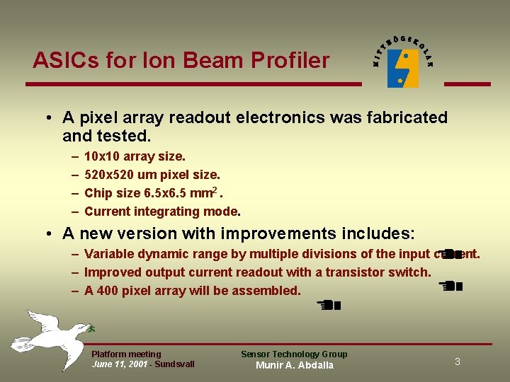
ASICs for Ion Beam Profiler • A pixel array readout electronics was fabricated and tested. – – 10 x 10 array size. 520 x 520 um pixel size. Chip size 6. 5 x 6. 5 mm 2. Current integrating mode. • A new version with improvements includes: – Variable dynamic range by multiple divisions of the input current. – Improved output current readout with a transistor switch. – A 400 pixel array will be assembled. Platform meeting June 11, 2001 - Sundsvall Sensor Technology Group Munir A. Abdalla 3
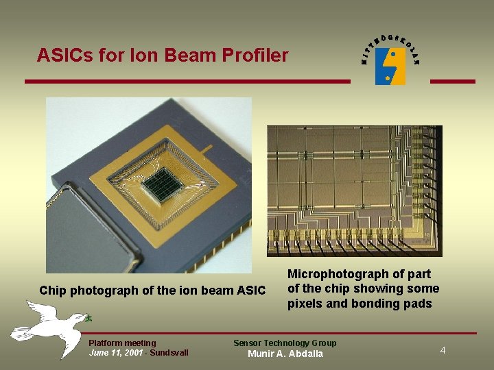
ASICs for Ion Beam Profiler Chip photograph of the ion beam ASIC Platform meeting June 11, 2001 - Sundsvall Microphotograph of part of the chip showing some pixels and bonding pads Sensor Technology Group Munir A. Abdalla 4
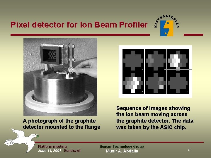
Pixel detector for Ion Beam Profiler A photograph of the graphite detector mounted to the flange Platform meeting June 11, 2001 - Sundsvall Sequence of images showing the ion beam moving across the graphite detector. The data was taken by the ASIC chip. Sensor Technology Group Munir A. Abdalla 5
Pixel Electronics for Photon Counting • A new biasing method for preamplifier-shapers, (IEEE ICECS’ 2 k). • An all-analogue time-walk free SCA for photon counting pixel sensors, (WSES/IEEE CSCC’ 2 k 1) • An All-digital window discriminator, (IEE Letters) • Low digital interference counter for photon counting pixels. Platform meeting June 11, 2001 - Sundsvall Sensor Technology Group Munir A. Abdalla 6
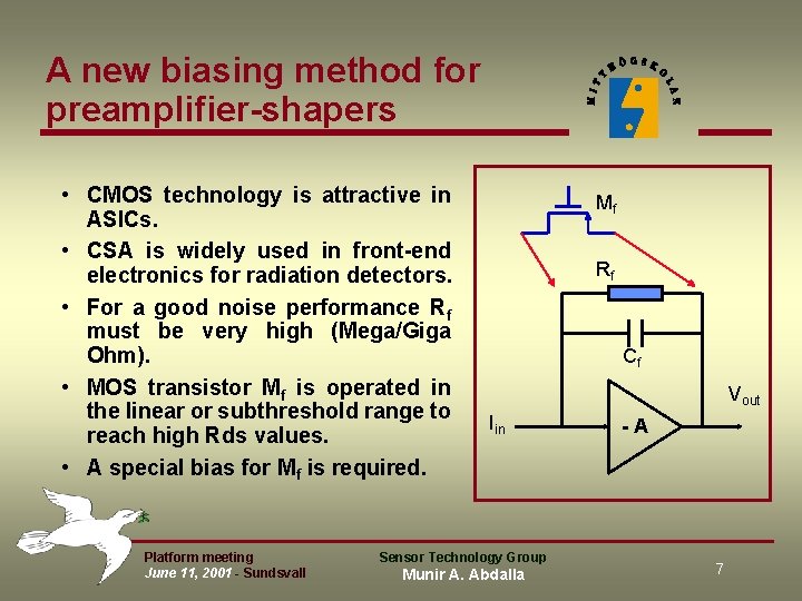
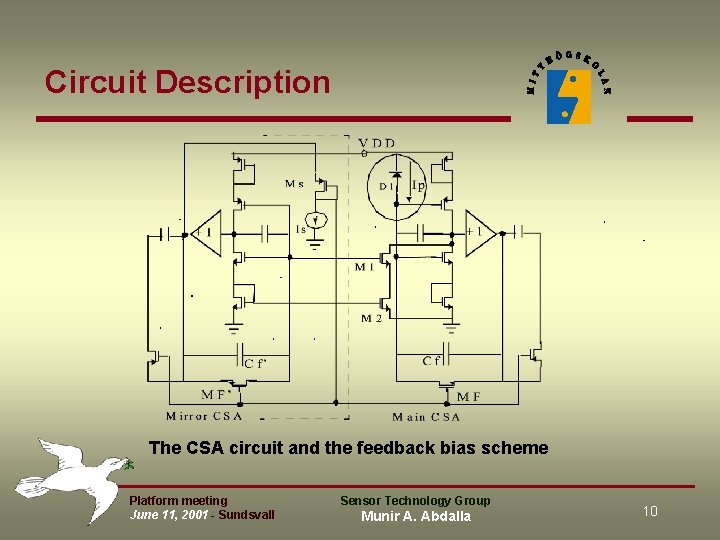
A new biasing method for preamplifier-shapers • CMOS technology is attractive in ASICs. • CSA is widely used in front-end electronics for radiation detectors. • For a good noise performance Rf must be very high (Mega/Giga Ohm). • MOS transistor Mf is operated in the linear or subthreshold range to reach high Rds values. • A special bias for Mf is required. Platform meeting June 11, 2001 - Sundsvall Mf Rf Cf Vout Iin Sensor Technology Group Munir A. Abdalla -A 7
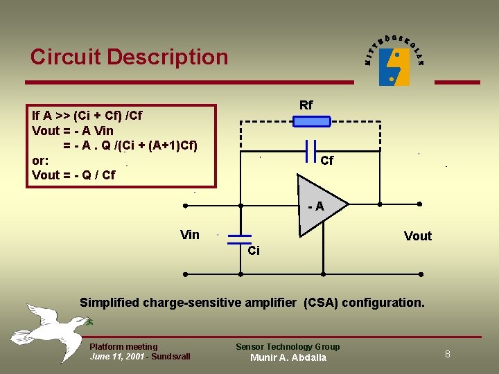
Circuit Description Rf If A >> (Ci + Cf) /Cf Vout = - A Vin = - A. Q /(Ci + (A+1)Cf) or: Vout = - Q / Cf Cf -A Vin Vout Ci Simplified charge-sensitive amplifier (CSA) configuration. Platform meeting June 11, 2001 - Sundsvall Sensor Technology Group Munir A. Abdalla 8
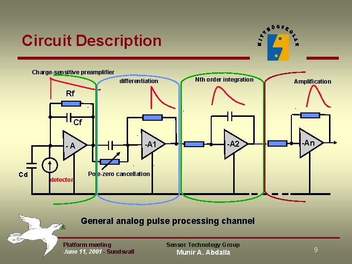
Circuit Description Charge-sensitive preamplifier differentiation Nth order integration Amplification Rf Cf -A 1 -A Cd detector -A 2 -An Pole-zero cancellation General analog pulse processing channel Platform meeting June 11, 2001 - Sundsvall Sensor Technology Group Munir A. Abdalla 9
Circuit Description The CSA circuit and the feedback bias scheme Platform meeting June 11, 2001 - Sundsvall Sensor Technology Group Munir A. Abdalla 10
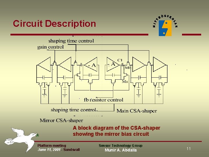
Circuit Description A block diagram of the CSA-shaper showing the mirror bias circuit Platform meeting June 11, 2001 - Sundsvall Sensor Technology Group Munir A. Abdalla 11
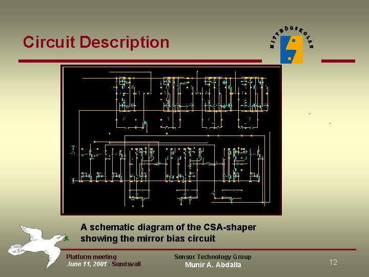
Circuit Description A schematic diagram of the CSA-shaper showing the mirror bias circuit Platform meeting June 11, 2001 - Sundsvall Sensor Technology Group Munir A. Abdalla 12
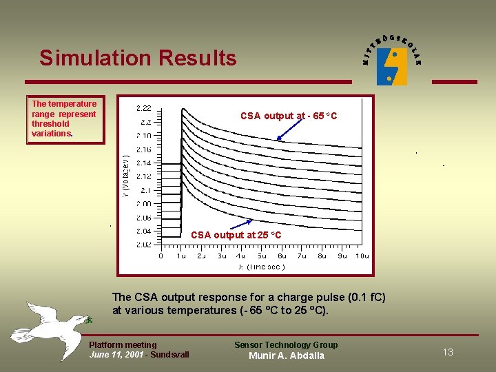
Simulation Results The temperature range represent threshold variations. CSA output at - 65 o. C CSA output at 25 o. C The CSA output response for a charge pulse (0. 1 f. C) at various temperatures (- 65 o. C to 25 o. C). Platform meeting June 11, 2001 - Sundsvall Sensor Technology Group Munir A. Abdalla 13
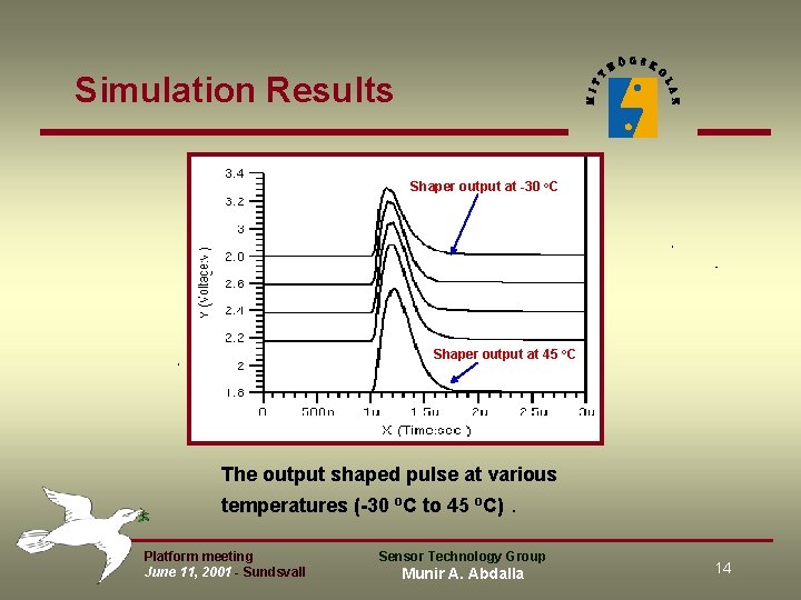
Simulation Results Shaper output at -30 o. C Shaper output at 45 o. C The output shaped pulse at various temperatures (-30 o. C to 45 o. C) Platform meeting June 11, 2001 - Sundsvall . Sensor Technology Group Munir A. Abdalla 14
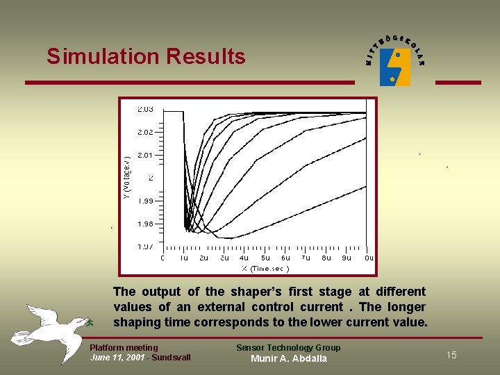
Simulation Results The output of the shaper’s first stage at different values of an external control current. The longer shaping time corresponds to the lower current value. Platform meeting June 11, 2001 - Sundsvall Sensor Technology Group Munir A. Abdalla 15
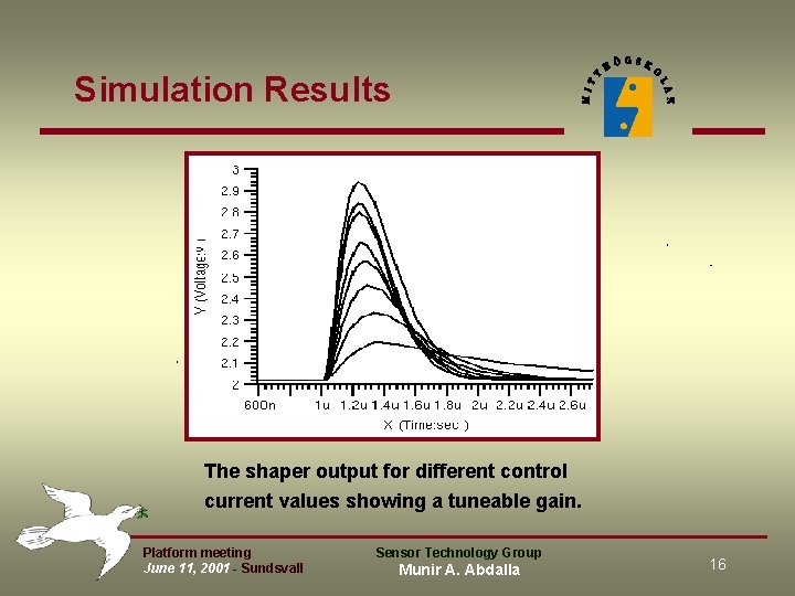
Simulation Results The shaper output for different control current values showing a tuneable gain. Platform meeting June 11, 2001 - Sundsvall Sensor Technology Group Munir A. Abdalla 16
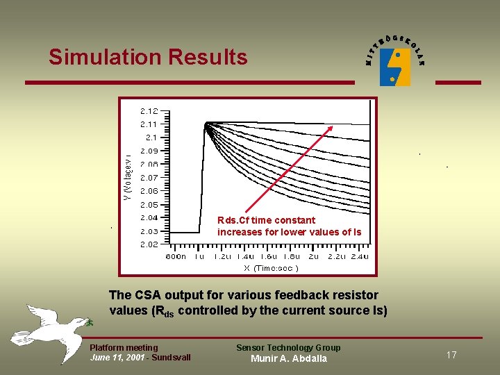
Simulation Results Rds. Cf time constant increases for lower values of Is The CSA output for various feedback resistor values (Rds controlled by the current source Is) Platform meeting June 11, 2001 - Sundsvall Sensor Technology Group Munir A. Abdalla 17
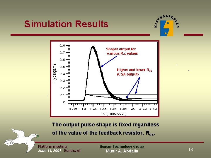
Simulation Results Shaper output for various Rds values Higher and lower Rds (CSA output) The output pulse shape is fixed regardless of the value of the feedback resistor, Rds. Platform meeting June 11, 2001 - Sundsvall Sensor Technology Group Munir A. Abdalla 18
An all-analogue SCA for photon counting pixels Schematic diagram of the all-analog SCA Platform meeting June 11, 2001 - Sundsvall Sensor Technology Group Munir A. Abdalla 19
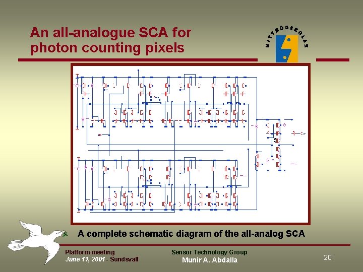
An all-analogue SCA for photon counting pixels A complete schematic diagram of the all-analog SCA Platform meeting June 11, 2001 - Sundsvall Sensor Technology Group Munir A. Abdalla 20
Conclusions • The scintillator-coated pixel sensor using a p-diff/n-well photosensor with an in-pixel preamplifier has the best performance (good sensitivity and low noise). • The ASIC chip for ion beam profiling will be modified to allow a flexible dynamic range by employing a current gain control. A better output current readout control will be implemented. • Circuit mirroring is an efficient method for achieving a stable operation of MOS transistors in the non-saturation mode by providing respectively adaptive nodes that vary in the same manner as the main circuit. Platform meeting June 11, 2001 - Sundsvall Sensor Technology Group Munir A. Abdalla 21
Conclusions • An all-analog pixel design would result in a reduced pixel size and low electronic noise. It will also result in a higher readout speed since the serial data shifting of the traditional in-pixel counter is eliminated. • The implementation of an asynchronous design of the window discriminator logic will achieve an overall areaefficient photon counting pixel. . • The design of a prescaled shift-counter in a photon counting pixel significantly reduces the noise caused by the switching activity of the digital part in the pixel circuit. Platform meeting June 11, 2001 - Sundsvall Sensor Technology Group Munir A. Abdalla 22