Rapid Prototyping Using Field Programmable Devices Allen C

Rapid Prototyping Using Field Programmable Devices Allen C. -H. Wu Department of Computer Science Tsing Hua University Hsinchu, Taiwan 30043, ROC email: chunghaw@cs. nthu. edu. tw 1
Outline Introduction to programmable logic devices and rapid prototyping. l FPGA design technologies and applications. l Logic emulation. l Reconfigurable computing and systems. l 2
Part I Introduction to Programmable Logic Devices and Rapid Prototyping 3
Programmable Logic Devices SPLDs (simple PLDs). l CPLDs (complex PLDs). l FPGAs (field programmable gate arrays). l SPGAs (system-programmable gate arrays). l 4
Programmable Interconnect Components FPID: I-Cube. - Dynamic switching. - Communication switches, network routes. - 32 -320 programmable I/O ports. - Up to 150 MHz clock frequency. l FPIC: Aptix. - 1024 programmable I/O ports. l 5
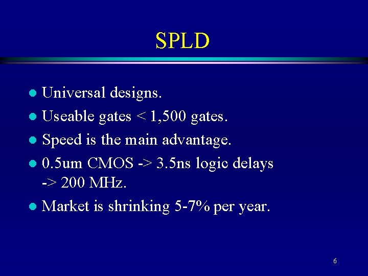
SPLD Universal designs. l Useable gates < 1, 500 gates. l Speed is the main advantage. l 0. 5 um CMOS -> 3. 5 ns logic delays -> 200 MHz. l Market is shrinking 5 -7% per year. l 6
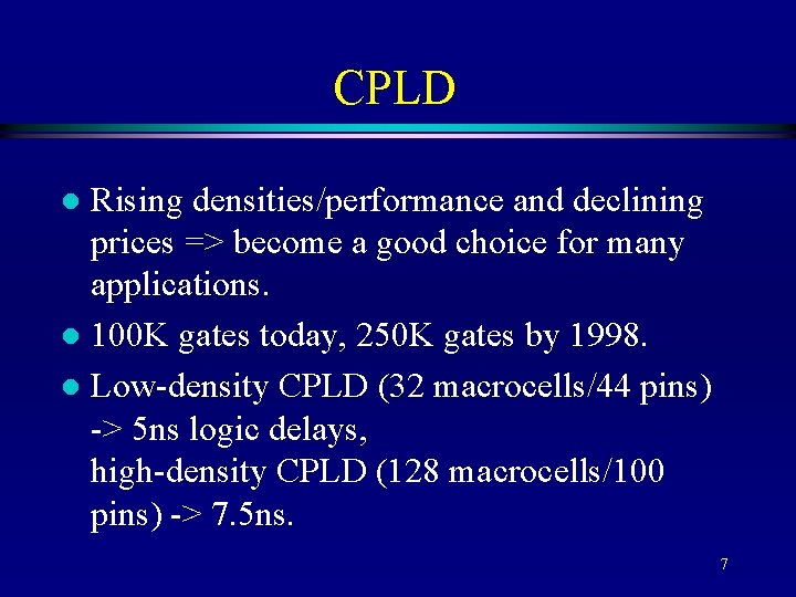
CPLD Rising densities/performance and declining prices => become a good choice for many applications. l 100 K gates today, 250 K gates by 1998. l Low-density CPLD (32 macrocells/44 pins) -> 5 ns logic delays, high-density CPLD (128 macrocells/100 pins) -> 7. 5 ns. l 7
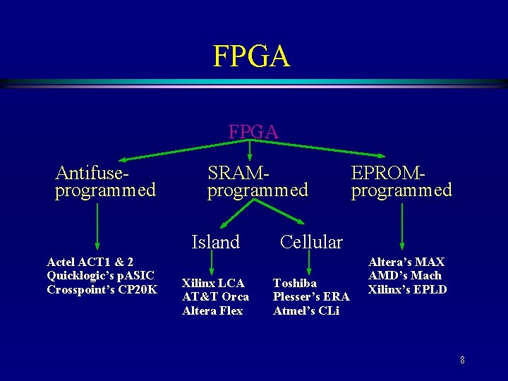
FPGA Antifuseprogrammed SRAMprogrammed Island Actel ACT 1 & 2 Quicklogic’s p. ASIC Crosspoint’s CP 20 K Xilinx LCA AT&T Orca Altera Flex EPROMprogrammed Cellular Toshiba Plesser’s ERA Atmel’s CLi Altera’s MAX AMD’s Mach Xilinx’s EPLD 8
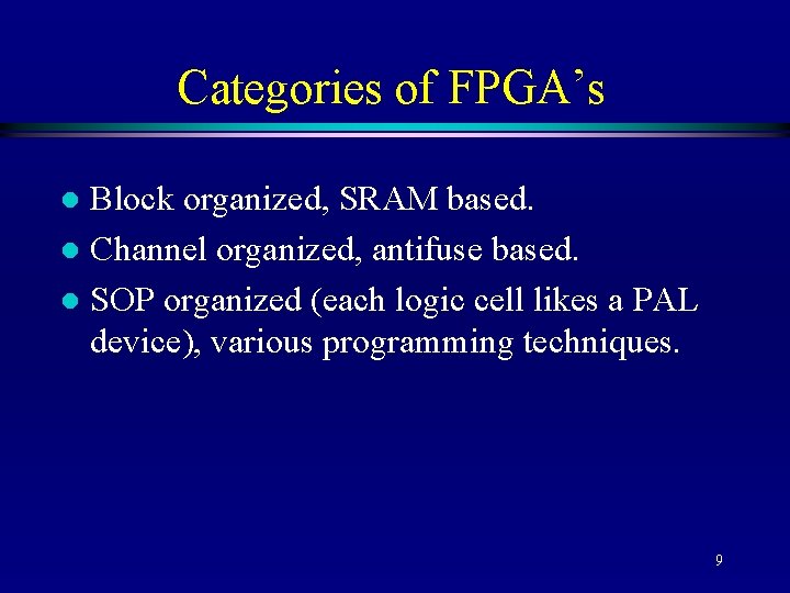
Categories of FPGA’s Block organized, SRAM based. l Channel organized, antifuse based. l SOP organized (each logic cell likes a PAL device), various programming techniques. l 9
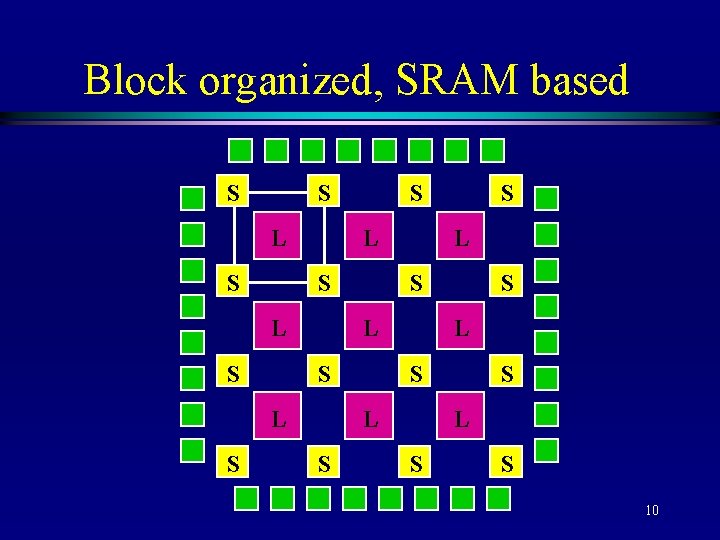
Block organized, SRAM based S S L S L S S L L L S S S L S S 10
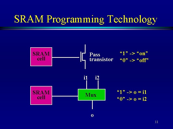
SRAM Programming Technology SRAM cell Pass transistor i 1 SRAM cell “ 1” -> “on” “ 0” -> “off” i 2 Mux “ 1” -> o = i 1 “ 0” -> o = i 2 o 11
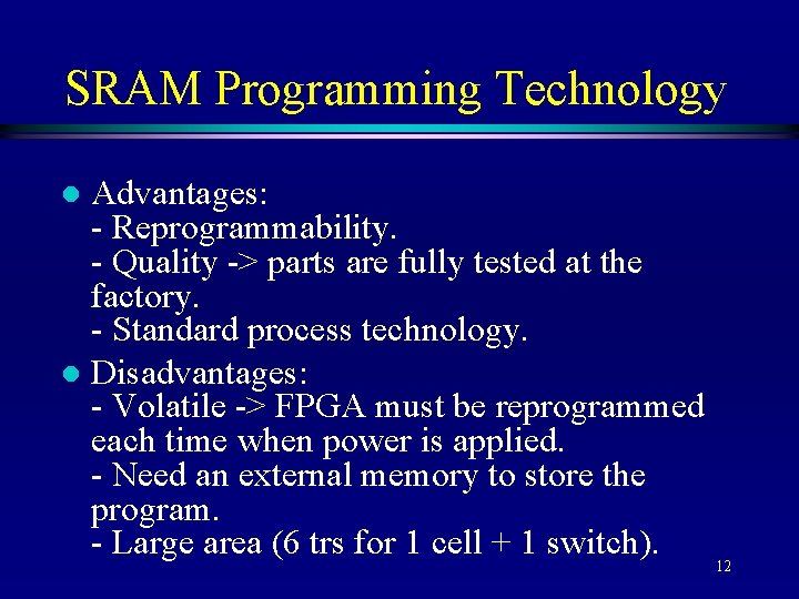
SRAM Programming Technology Advantages: - Reprogrammability. - Quality -> parts are fully tested at the factory. - Standard process technology. l Disadvantages: - Volatile -> FPGA must be reprogrammed each time when power is applied. - Need an external memory to store the program. - Large area (6 trs for 1 cell + 1 switch). l 12
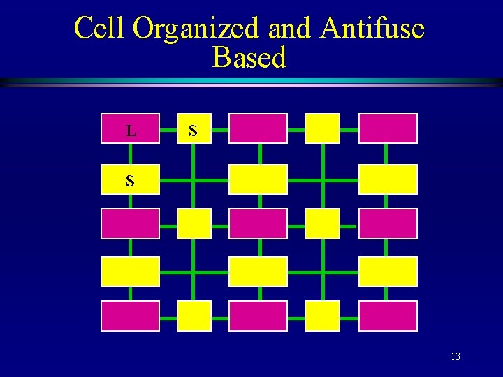
Cell Organized and Antifuse Based L S S 13
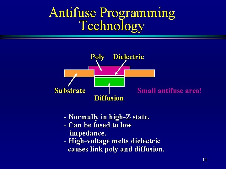
Antifuse Programming Technology Poly Substrate Dielectric Diffusion Small antifuse area! - Normally in high-Z state. - Can be fused to low impedance. - High-voltage melts dielectric causes link poly and diffusion. 14
EPROM/EEPROM Technology EPROM can be reprogrammed, no need for external storage. l EPROM can not be re-programmed in circuit. l EEPROM can be re-programmed in circuit. l EEPROM consumes 2 X more area as EPROM. l 15
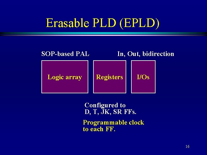
Erasable PLD (EPLD) SOP-based PAL Logic array In, Out, bidirection Registers I/Os Configured to D, T, JK, SR FFs. Programmable clock to each FF. 16
Programming the FPGA Configuration. l Readback - design verification and debugging. l Security - a security-bit to prevent readback. l 17
Advantages and Disadvantages of FPGA Fast turnaround. l Low NRE (non-recurring engineering) changes. l Low risk. l Effective design verification. l low testing cost. l Chip size & cost. l Slow speed. l 18
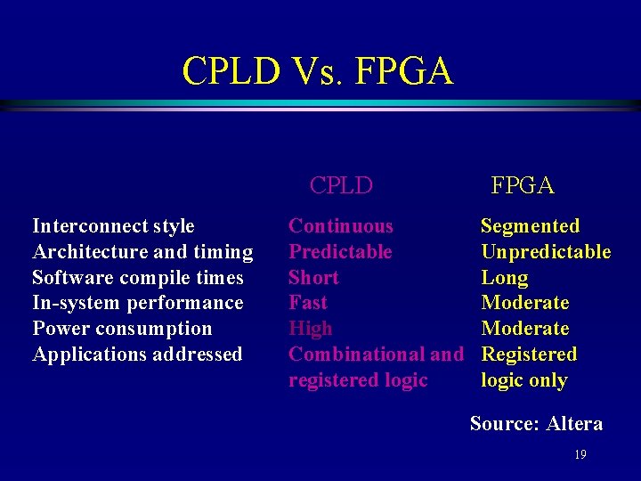
CPLD Vs. FPGA CPLD Interconnect style Architecture and timing Software compile times In-system performance Power consumption Applications addressed Continuous Predictable Short Fast High Combinational and registered logic FPGA Segmented Unpredictable Long Moderate Registered logic only Source: Altera 19
FPGA Selection Criteria Density. l Speed. l Price. l Flexibility. l 20
SPGA Allow multiple building blocks. l Logic. l Memory. l Data path. l 21
Applications Using SPGAs Intellectual property (IP). l Communication & networking. l Graphical processing. l Embedded processing. l 22
Designing with SPGAs A team-based approach. l Understanding how to use SPGA system features will be the key to pulling the entire design into a single device. l 23
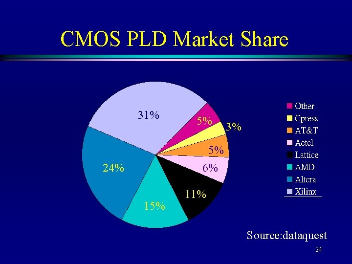
CMOS PLD Market Share 31% 5% 3% 5% 6% 24% 15% 11% Source: dataquest 24
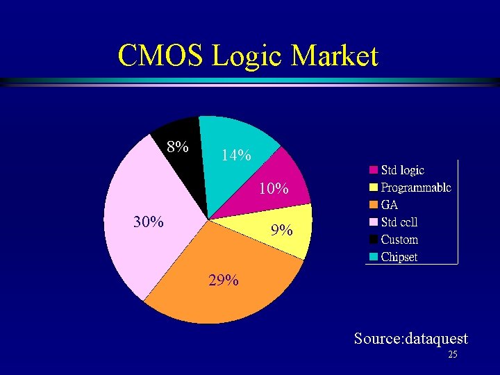
CMOS Logic Market 8% 14% 10% 30% 9% 29% Source: dataquest 25
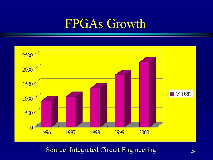
FPGAs Growth Source: Integrated Circuit Engineering 26
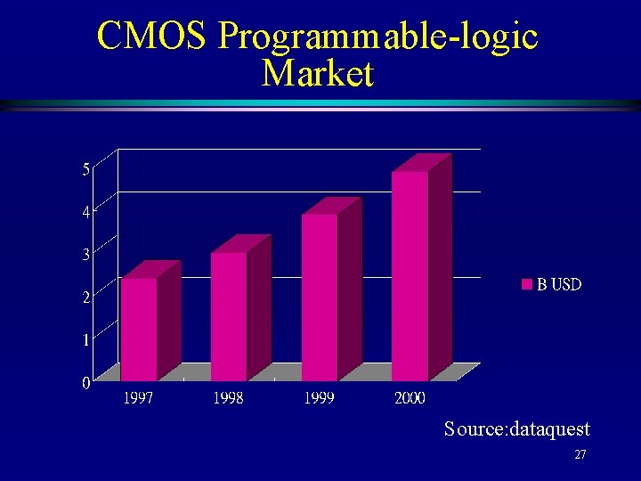
CMOS Programmable-logic Market Source: dataquest 27
Rapid Prototyping What? l Why? l How? l 28
What is prototyping? Basic components: FPGAs and FPICs. l Hardware : boards, boxes, and cabinets. l Software: methodologies and CAD tools. l 29
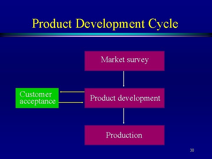
Product Development Cycle Market survey Customer acceptance Product development Production 30
Pressures on Today’s Product Development Time-to-market! l Design complexity! l 31
Why Needs Prototyping? Design verification. l Limited production. l Concurrent engineering. l 32
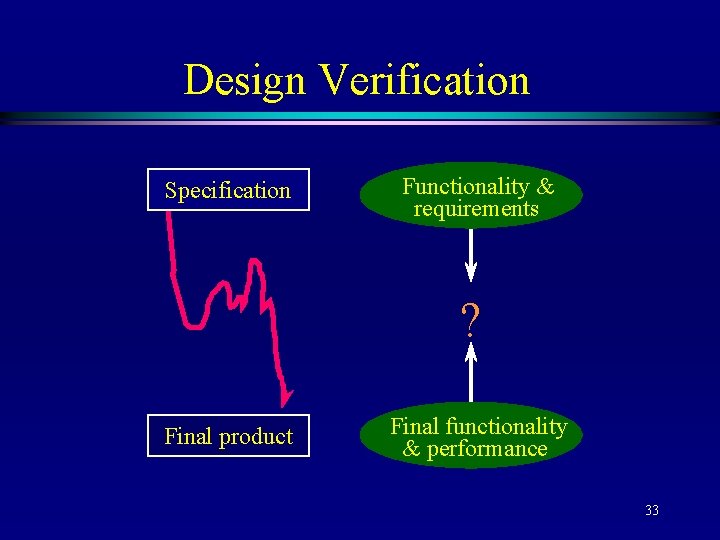
Design Verification Specification Functionality & requirements ? Final product Final functionality & performance 33
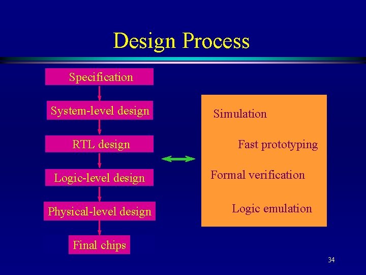
Design Process Specification System-level design RTL design Logic-level design Physical-level design Simulation Fast prototyping Formal verification Logic emulation Final chips 34
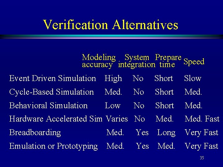
Verification Alternatives Modeling System Prepare accuracy integration time Speed Event Driven Simulation High No Short Slow Cycle-Based Simulation Med. No Short Med. Behavioral Simulation Low No Short Med. Hardware Accelerated Sim Varies No Med. Fast Breadboarding Med. Yes Long Very Fast Emulation or Prototyping Med. Yes Med. Very Fast 35
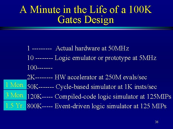
A Minute in the Life of a 100 K Gates Design 1 ----- Actual hardware at 50 MHz 10 ---- Logic emulator or prototype at 5 MHz 100 ------2 K---- HW accelerator at 250 M evals/sec 1 Mon. 50 K------- Cycle-based simulator at 1 K insts/sec 3 Mon. 120 K----- Compiled-code logic simulator at 125 MIPs 1. 5 Yr. 800 K----- Event-driven logic simulator at 125 MIPs 36
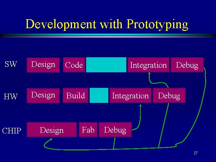
Development with Prototyping SW Design Code HW Design Build CHIP Design Fab Integration Debug 37
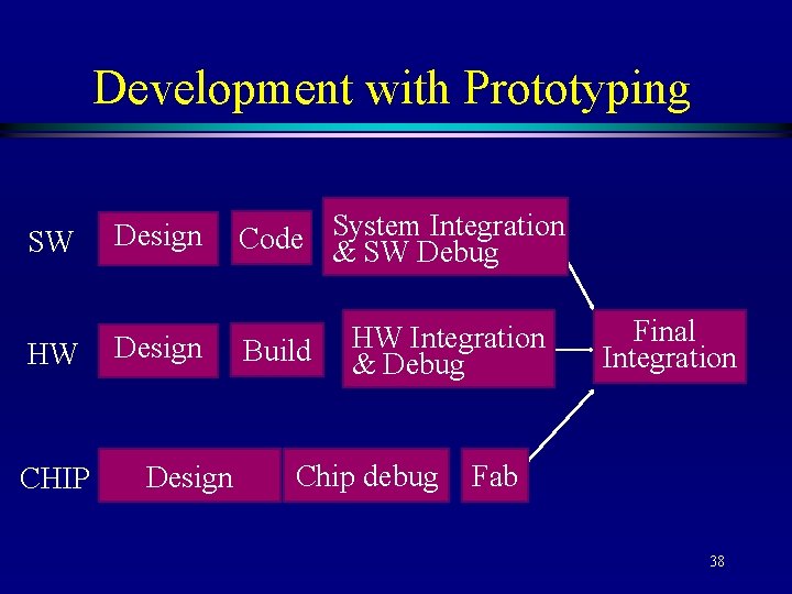
Development with Prototyping SW HW CHIP Design Integration Code System & SW Debug Build HW Integration & Debug Chip debug Final Integration Fab 38
How to Develop a Prototyping using FPDs Custom-designed prototyping board. l Logic-emulation systems. l Field-programmable printed-circuit-boards. l 39
Part II FPGA Design Technologies and Applications 40
FPGAs What? - Programmable logic + programmable routing = FPGAs. l Why? - Zero NREs, easy bug fixes, and short time-to-market. l How? l 41
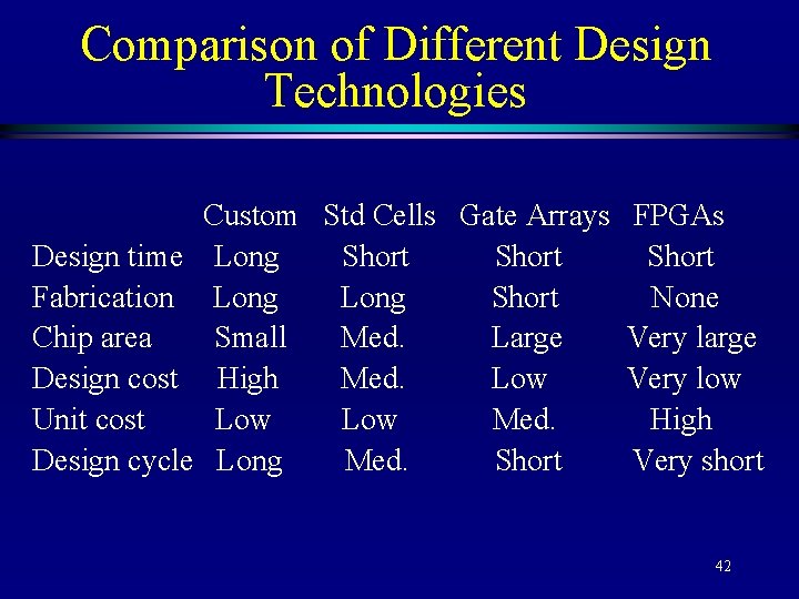
Comparison of Different Design Technologies Design time Fabrication Chip area Design cost Unit cost Design cycle Custom Std Cells Gate Arrays Long Short Small Med. Large High Med. Low Low Med. Long Med. Short FPGAs Short None Very large Very low High Very short 42
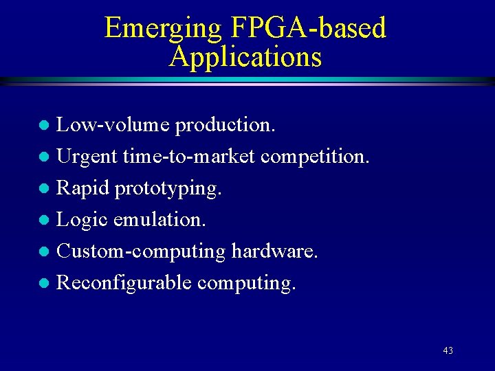
Emerging FPGA-based Applications Low-volume production. l Urgent time-to-market competition. l Rapid prototyping. l Logic emulation. l Custom-computing hardware. l Reconfigurable computing. l 43
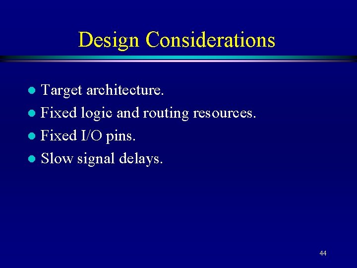
Design Considerations Target architecture. l Fixed logic and routing resources. l Fixed I/O pins. l Slow signal delays. l 44
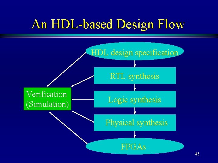
An HDL-based Design Flow HDL design specification RTL synthesis Verification (Simulation) Logic synthesis Physical synthesis FPGAs 45
Design Specification HDLs - VHDL and Verilog. l Why needs an HDL-based design methodology? l Target Applications. l Coding Styles. l Design representation. l Design entry. l 46
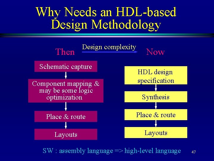
Why Needs an HDL-based Design Methodology Then Design complexity Schematic capture Component mapping & may be some logic optimization Now HDL design specification Synthesis Place & route Layouts SW : assembly language => high-level language 47
Target Applications and Layout Architectures l l l Datapath dominated designs : DSPs and processors. Control dominated designs: controllers and communication chips. Mixed type of designs. l l Bit-sliced stacks. Standard cells. Macro-cell-based. FPGAs. 48
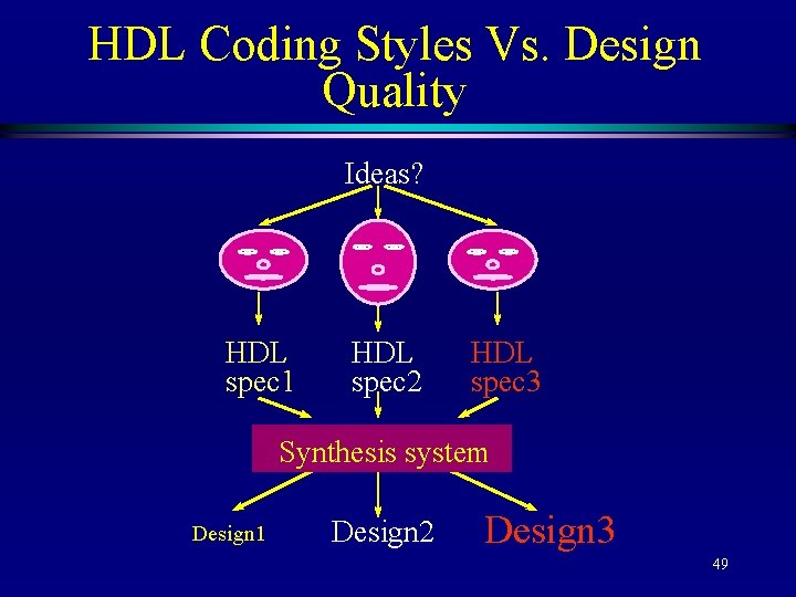
HDL Coding Styles Vs. Design Quality Ideas? HDL spec 1 HDL spec 2 HDL spec 3 Synthesis system Design 1 Design 2 Design 3 49
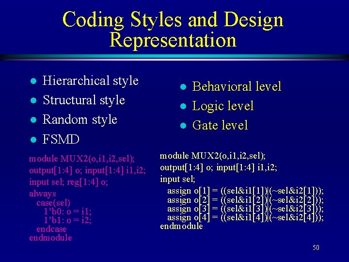
Coding Styles and Design Representation l l Hierarchical style Structural style Random style FSMD module MUX 2(o, i 1, i 2, sel); output[1: 4] o; input[1: 4] i 1, i 2; input sel; reg[1: 4] o; always case(sel) 1’b 0: o = i 1; 1’b 1: o = i 2; endcase endmodule l l l Behavioral level Logic level Gate level module MUX 2(o, i 1, i 2, sel); output[1: 4] o; input[1: 4] i 1, i 2; input sel; assign o[1] = ((sel&i 1[1])|(~sel&i 2[1])); assign o[2] = ((sel&i 1[2])|(~sel&i 2[2])); assign o[3] = ((sel&i 1[3])|(~sel&i 2[3])); assign o[4] = ((sel&i 1[4])|(~sel&i 2[4])); endmodule 50
RTL Synthesis HDL compilation. l Design representation. l Component selection. l Component generation. l Resource sharing. l 51
Logic Synthesis Logic minimization. l Technology dependent/independent minimization. l Technology mapping. l 52
Physical Synthesis Placement. l Routing. l 53
Logic Synthesis Problems for FPGAs How to synthesize a logic network to realize a given function. l How to realize a logic network using FPGAs. l How to optimize a given network for area and timing. l How to synthesize routable circuits. l How to solve these problems efficiently. l 54
Representation of Boolean Functions Truth tables. l Factored forms: SOP and POS. l BDD. l Boolean networks. l 55
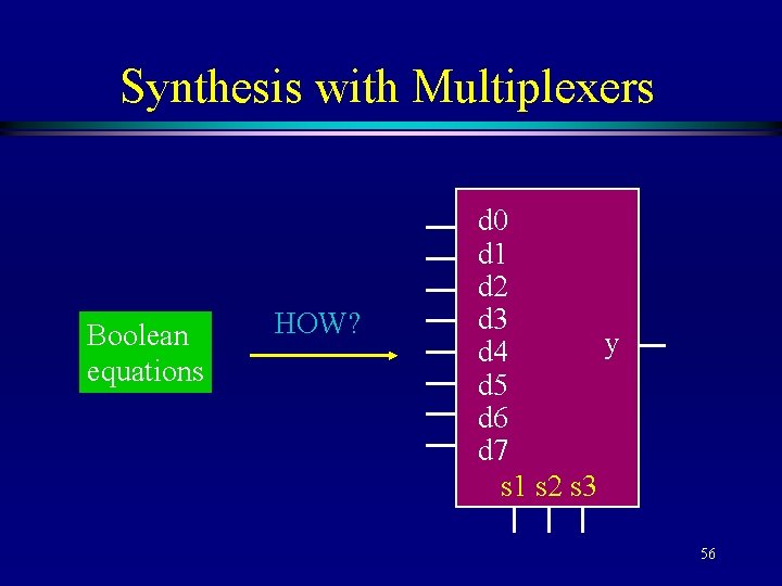
Synthesis with Multiplexers Boolean equations HOW? d 0 d 1 d 2 d 3 y d 4 d 5 d 6 d 7 s 1 s 2 s 3 56
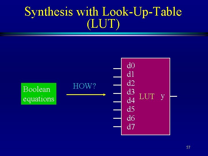
Synthesis with Look-Up-Table (LUT) Boolean equations HOW? d 0 d 1 d 2 d 3 LUT y d 4 d 5 d 6 d 7 57
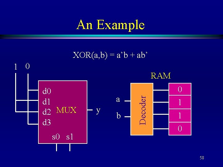
An Example XOR(a, b) = a’b + ab’ 1 0 d 1 d 2 MUX d 3 s 0 s 1 a y b Decoder RAM 0 1 1 0 58
Multilevel Logic Minimization MIS and SIS by UC Berkeley. l Optimization for timing, area, and power. l Technology independent. l 59
Technology Mapping for FPGAs Technology mapping is the process of binding technology dependent circuits to technology independent circuits. l Technology mapping for FPGAs consists of two steps: (1) decomposition and (2) covering. l Technology mapper optimizes the final circuit by selecting sub-networks which are covered by LUTs. l 60
Technology Mapping for FPGAs LUTs have fixed number of inputs, k-input, which can implement logic functions up to k variables. l Nodes and sub-networks with at most k inputs in a Boolean network are referred to feasible nodes and sub-networks else infeasible. l Infeasible nodes need to be decomposed into a set of feasible nodes so that a circuit covering the network exists. 61 l
Technology Mapping for FPGAs l An FPGA-based technology mapper performs three tasks: 1. Decomposition - It decomposes infeasible expressions into feasible ones. 2. Reduction - It groups small expressions into CLBs to promote sharing of resources. 3. Packing - It allocates CLBs to expressions that cannot be shared. 62
Technology Mapping for FPGAs l The optimization goals for FPGA-based technology mapping include: 1. The number of CLBs, 2. The number of levels of CLB circuits, and 3. Routable designs. 63
Decomposition l Decomposition consists of three steps: 1. Identify divisors which are common to many functions. 2. Introduce the divisor as a new node. 3. Re-express existing nodes using the new nodes. 64
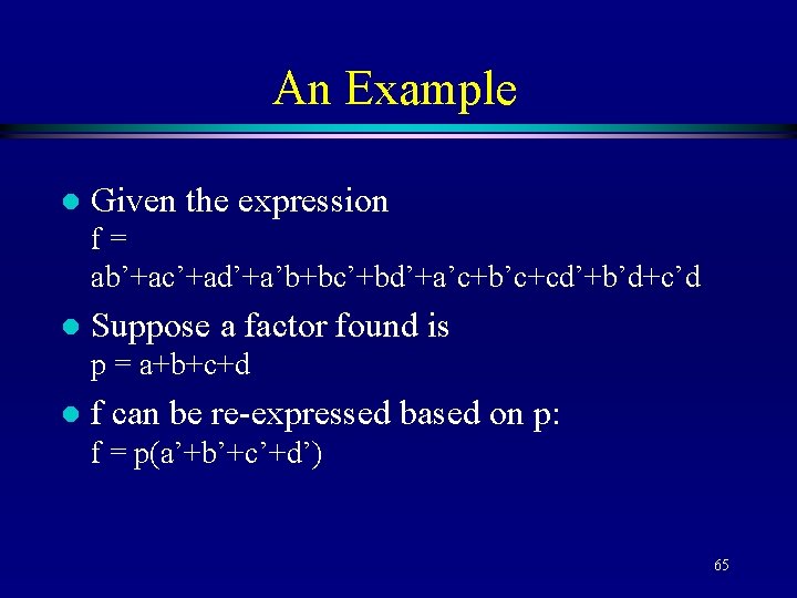
An Example l Given the expression f= ab’+ac’+ad’+a’b+bc’+bd’+a’c+b’c+cd’+b’d+c’d l Suppose a factor found is p = a+b+c+d l f can be re-expressed based on p: f = p(a’+b’+c’+d’) 65
Decomposition Techniques Disjoint decomposition. l Shannon cofactoring. l Roth-Karp decomposition. l Algebraic decomposition. l AND-OR decomposition. l 66
Disjoint Decomposition Disjoint decomposition can be found by searching through all possible partitions of inputs to the infeasible nodes, and using well known methods, such as residues, to determine if each partition leads to a disjoint decomposition. l Disadvantage: the number of partitions grows exponentially with number of inputs to the infeasible nodes. l 67
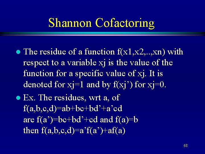
Shannon Cofactoring The residue of a function f(x 1, x 2, . . , xn) with respect to a variable xj is the value of the function for a specific value of xj. It is denoted for xj=1 and by f(xj’) for xj=0. l Ex. The residues, wrt a, of f(a, b, c, d)=ab+bc+bd’+a’cd are f(a’)=bc+bd’+cd and f(a)=b then f(a, b, c, d)=a’f(a’)+af(a) l 68
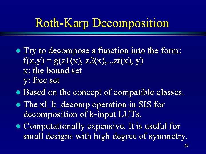
Roth-Karp Decomposition Try to decompose a function into the form: f(x, y) = g(z 1(x), z 2(x), . . , zt(x), y) x: the bound set y: free set l Based on the concept of compatible classes. l The xl_k_decomp operation in SIS for decomposition of k-input LUTs. l Computationally expensive. It is useful for small designs with high degree of symmetry. l 69
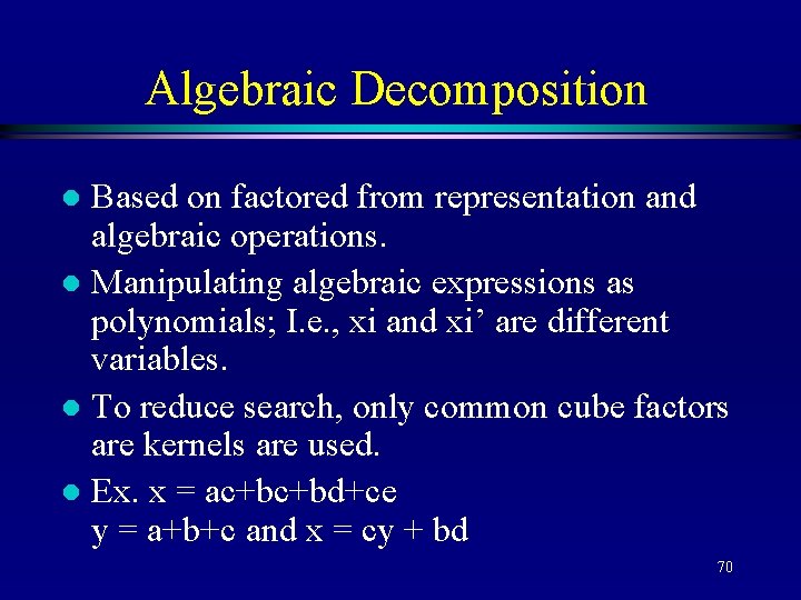
Algebraic Decomposition Based on factored from representation and algebraic operations. l Manipulating algebraic expressions as polynomials; I. e. , xi and xi’ are different variables. l To reduce search, only common cube factors are kernels are used. l Ex. x = ac+bc+bd+ce y = a+b+c and x = cy + bd l 70
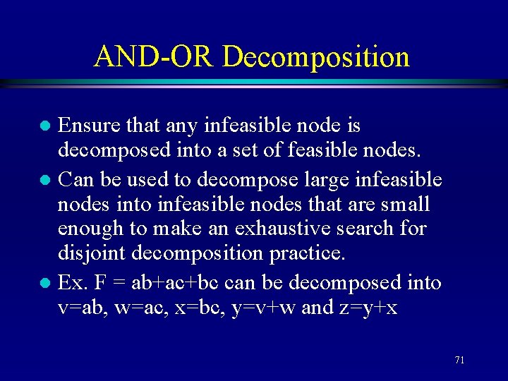
AND-OR Decomposition Ensure that any infeasible node is decomposed into a set of feasible nodes. l Can be used to decompose large infeasible nodes into infeasible nodes that are small enough to make an exhaustive search for disjoint decomposition practice. l Ex. F = ab+ac+bc can be decomposed into v=ab, w=ac, x=bc, y=v+w and z=y+x l 71
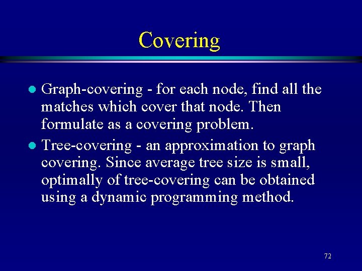
Covering Graph-covering - for each node, find all the matches which cover that node. Then formulate as a covering problem. l Tree-covering - an approximation to graph covering. Since average tree size is small, optimally of tree-covering can be obtained using a dynamic programming method. l 72
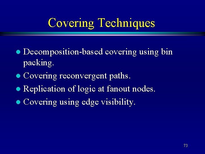
Covering Techniques Decomposition-based covering using bin packing. l Covering reconvergent paths. l Replication of logic at fanout nodes. l Covering using edge visibility. l 73
Tree-based Technology Mapping Methods Chortle, Chortle-crf, and Chortle-d. l Hydra. l TM-based on edge visibility. l mis-PGA. l 74
Graph-Based Technology Mapping Methods DAG-Map. l Flow-Map. l Area/depth trade-off. l 75
Layout-Driven FPGA Synthesis Mapping directed synthesis. l Mapping with resynthesis. l Combining technology mapping and placement. l Routability-driven technology mapping. l 76
Performance-Driven Methods mis-pga (xln_p) - mapping with synthesis. Logic synthesis during a timing driven placement. l M. map - interwinded mapping and placement procedures by taking into account wiring delays. l 77
Routability-Driven Methods Alternative wires - attempt to identify alternative wires and alternative functions for wires that cannot be routed due to the limited routing resources. l Balanced routing resources and cell resources by trading off the routability with the compactness of a design. Try to deliver routable designs by controlling directly the pins-per-cell ratio of the design. l 78
Sequential Synthesis for FPGAs Each CLB has two FFs. l Not much work has done in this area. WHY? l Two attempts were conducted by the UCB group: map combinational and sequential circuits simultaneously and separately. l How the Xilinx’s APR handles the sequential circuits? l 79
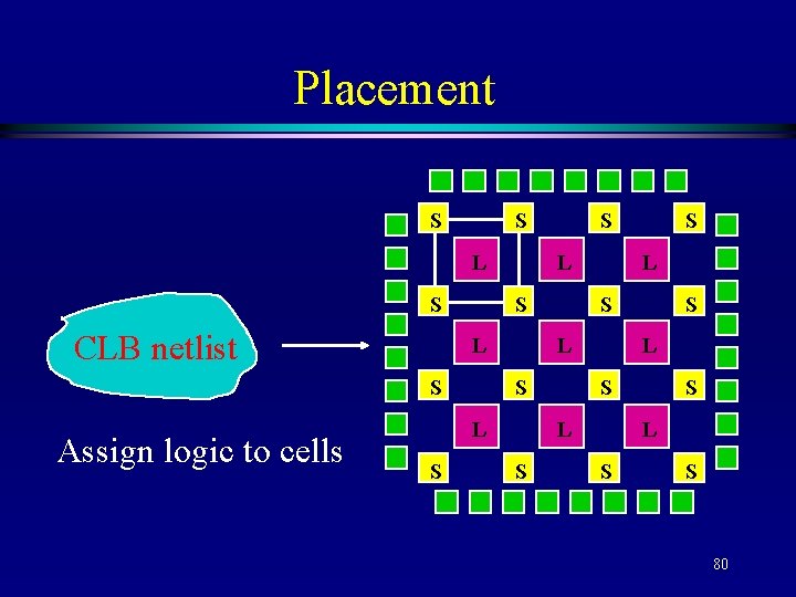
Placement S S L S CLB netlist L S Assign logic to cells S S S L L L S S S L S S 80
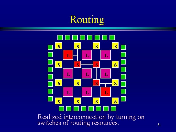
Routing S S L S L S S L L L S S S L S S Realized interconnection by turning on switches of routing resources. 81
Placement & Routing Methods Placement - simulated annealing is the commonly used method. l Routing - routability-driven and timingdriven. l Time-consuming design tasks. l Architectural dependent. l 82
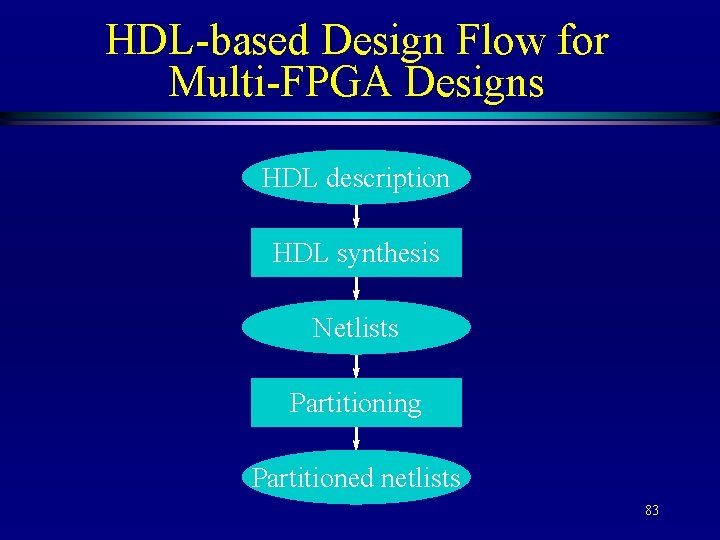
HDL-based Design Flow for Multi-FPGA Designs HDL description HDL synthesis Netlists Partitioning Partitioned netlists 83
Basic Partitioning Techniques The min-cut partitioning: The Kernighan-Lin algorithm. The Fiduccia and Mattheyses algorithm. The Krishnamurthy algorithm. l The ratio-cut algorithm. l A variety of clustering algorithms. l . . . 84
Multi-FPGA Partitioning Constraints: 1. Fixed number of I/O pins. 2. Fixed number of CLBs. 3. Utilization. l Objectives: 1. Cost minimization. 2. Delay minimization. l 85
Circuit-Level Partitioning Methods Multiway partitioning methods based on the min-cut algorithm. l Interconnect minimization by cell replication. l Clustering-based partitioning methods - cone. l Combining top-down partitioning and bottom-up clustering methods. l 86
Considerations for Multi-FPGA Partitioning Limited IO-pin and logic resources. l Logic utilization is predominated by IO-pin limitation. l How to alleviate the IO-limitation problem is the key to improve the logic utilization of FPGA chips. l 87
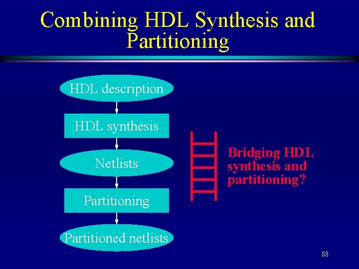
Combining HDL Synthesis and Partitioning HDL description HDL synthesis Netlists Bridging HDL synthesis and partitioning? Partitioning Partitioned netlists 88
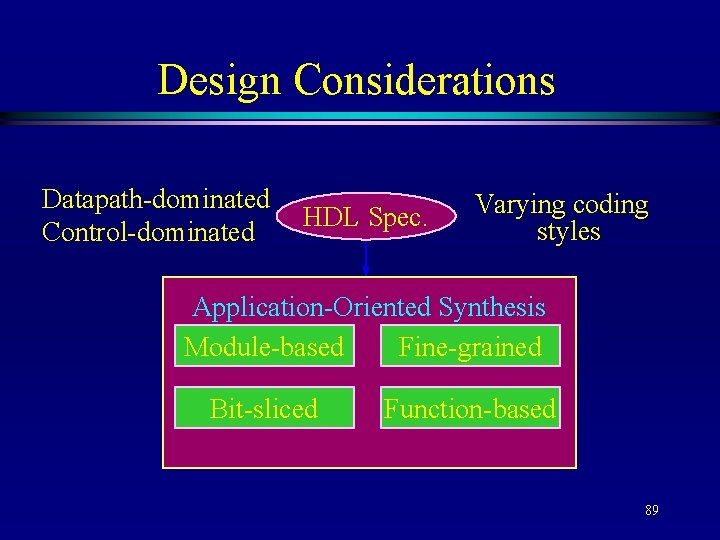
Design Considerations Datapath-dominated Control-dominated HDL Spec. Varying coding styles Application-Oriented Synthesis Module-based Fine-grained Bit-sliced Function-based 89
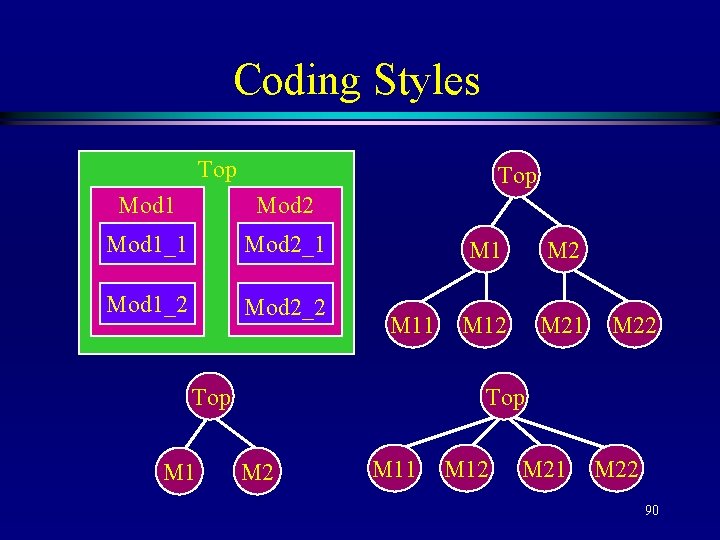
Coding Styles Top Mod 1 Mod 2 Mod 1_1 Mod 2_1 Mod 1_2 Mod 2_2 M 11 Top M 1 M 2 M 12 M 21 M 22 Top M 2 M 11 M 12 M 21 M 22 90
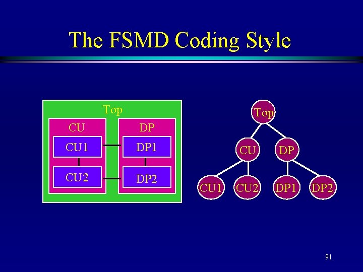
The FSMD Coding Style Top CU DP CU 1 DP 1 CU 2 DP 2 CU 1 CU DP CU 2 DP 1 DP 2 91
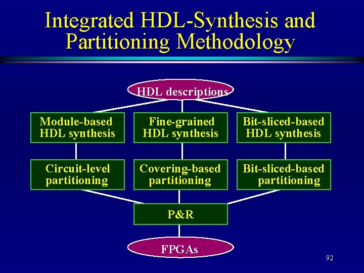
Integrated HDL-Synthesis and Partitioning Methodology HDL descriptions Module-based HDL synthesis Fine-grained HDL synthesis Bit-sliced-based HDL synthesis Circuit-level partitioning Covering-based partitioning Bit-sliced-based partitioning P&R FPGAs 92
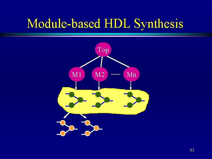
Module-based HDL Synthesis Top M 1 M 2 Mn 93
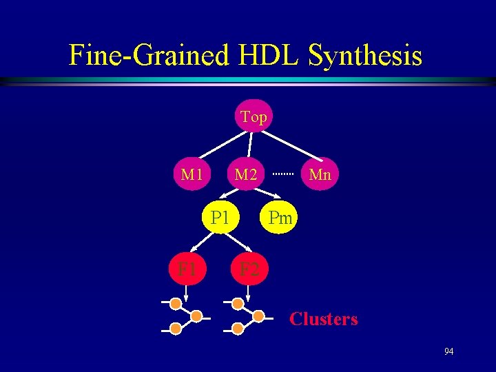
Fine-Grained HDL Synthesis Top M 1 M 2 P 1 F 1 Mn Pm F 2 Clusters 94
![A Process Example Process{P 1} input[0: 3] i 1, i 2; input i 3; A Process Example Process{P 1} input[0: 3] i 1, i 2; input i 3;](http://slidetodoc.com/presentation_image_h/1cc0b5f8095983417951fbbaa9a748df/image-95.jpg)
A Process Example Process{P 1} input[0: 3] i 1, i 2; input i 3; output[0: 3] o 1; output o 2; o 1 = i 1 + i 2; o 2 = i 1[0] & i 3; i 2 i 1 P 1 o 2 i 3 o 1[0] o 1[3] f 1. 0 f 1. 3 f 2 4 4 + & o 1 o 2 4 95
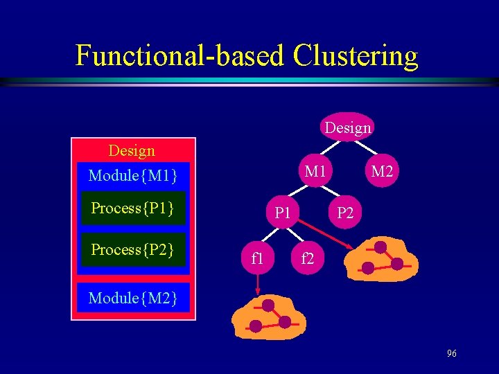
Functional-based Clustering Design Module{M 1} M 1 Process{P 1} Process{P 2} P 1 f 1 M 2 P 2 f 2 Module{M 2} 96
![Bit-Sliced-Based Synthesis [0] Mux[0: 7] Mux[0: 5] Adder[0: 7] [5] [7] Mux Adder 97 Bit-Sliced-Based Synthesis [0] Mux[0: 7] Mux[0: 5] Adder[0: 7] [5] [7] Mux Adder 97](http://slidetodoc.com/presentation_image_h/1cc0b5f8095983417951fbbaa9a748df/image-97.jpg)
Bit-Sliced-Based Synthesis [0] Mux[0: 7] Mux[0: 5] Adder[0: 7] [5] [7] Mux Adder 97
![Functional Clustering DP Mux [0] [7] Mux Adder DP[0] DP Mux[0] [0] Adder[0] [5] Functional Clustering DP Mux [0] [7] Mux Adder DP[0] DP Mux[0] [0] Adder[0] [5]](http://slidetodoc.com/presentation_image_h/1cc0b5f8095983417951fbbaa9a748df/image-98.jpg)
Functional Clustering DP Mux [0] [7] Mux Adder DP[0] DP Mux[0] [0] Adder[0] [5] Mux[7] [0] [7] DP[7] Adder[7] 98
Part III Logic Emulation 99
What is a Logic Emulation System A programmable hardware built with programmable logic and programmable interconnect devices. l A software which automatically programs the hardware according to the circuit under design. l Control HW/SW to support operation of the emulated design as a hardware component operating in real time. l 100
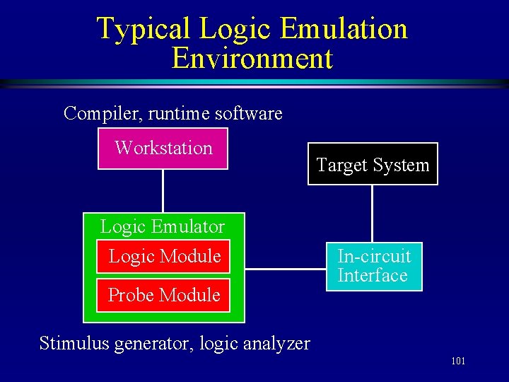
Typical Logic Emulation Environment Compiler, runtime software Workstation Logic Emulator Logic Module Probe Module Target System In-circuit Interface Stimulus generator, logic analyzer 101
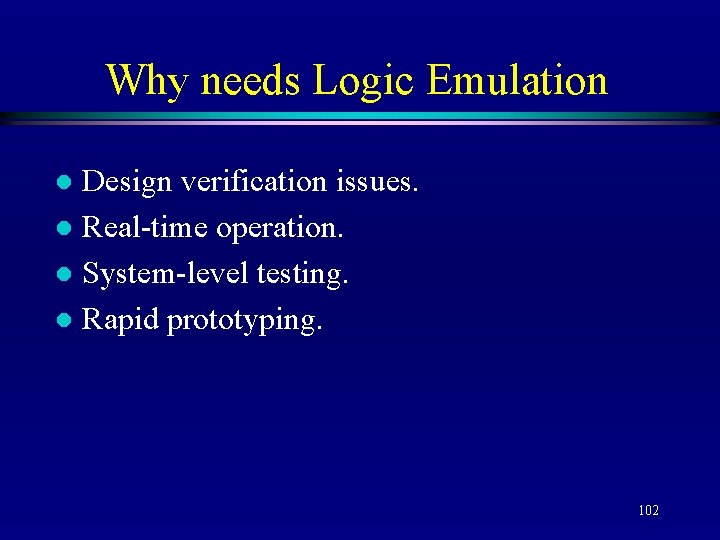
Why needs Logic Emulation Design verification issues. l Real-time operation. l System-level testing. l Rapid prototyping. l 102
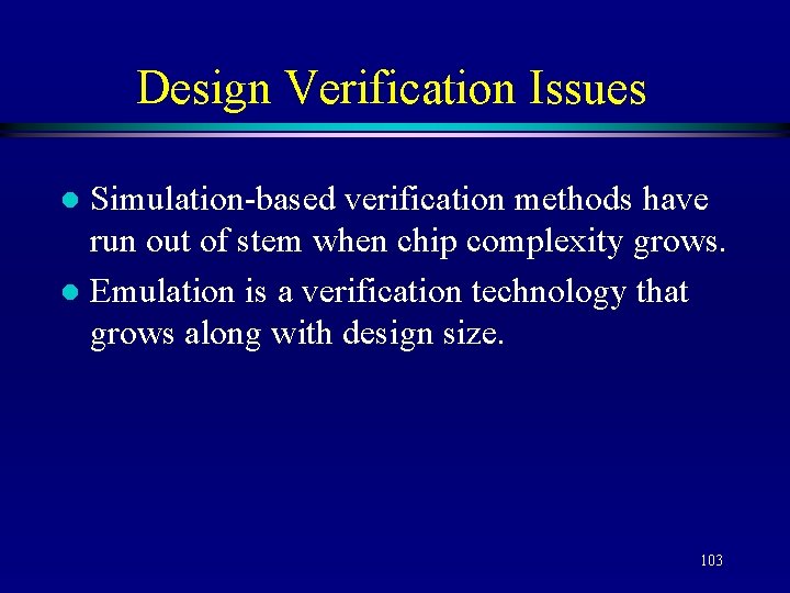
Design Verification Issues Simulation-based verification methods have run out of stem when chip complexity grows. l Emulation is a verification technology that grows along with design size. l 103
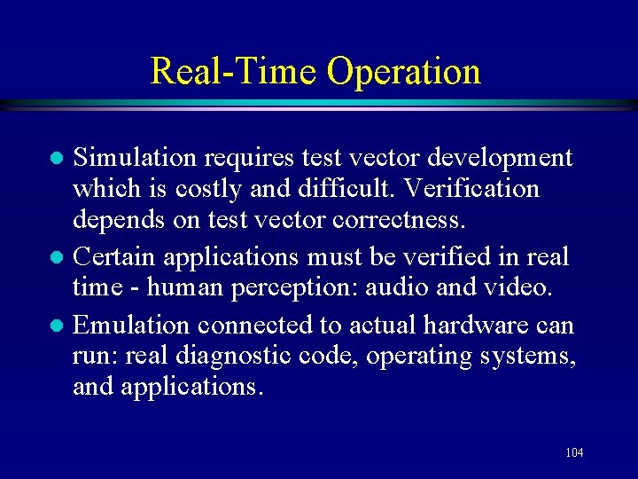
Real-Time Operation Simulation requires test vector development which is costly and difficult. Verification depends on test vector correctness. l Certain applications must be verified in real time - human perception: audio and video. l Emulation connected to actual hardware can run: real diagnostic code, operating systems, and applications. l 104
System-Level Testing Often the chip meets spec but fails in the system. l System-level interactions between the chip and other components. l Internal probing is impossible when the chip is fabbed and placed in a system, but it is possible using emulation. l 105
Rapid Prototyping Once emulated design is debugged it is available for immediate use by software developers for software debugging. l Emulated design is available for demo and experiments with architecture on real applications and data. l 106
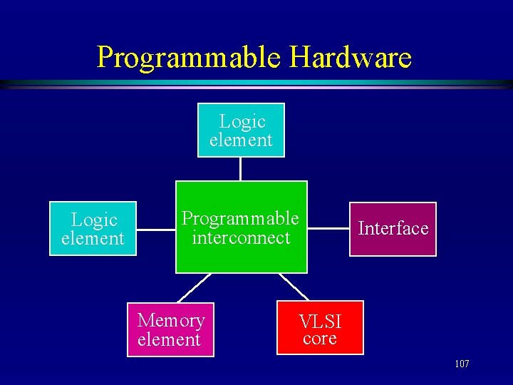
Programmable Hardware Logic element Programmable interconnect Memory element Interface VLSI core 107
Considerations The capacity of logic and interconnection depends on package constraints. This forces a hierarchical system. Chips => boards => boxes => system l The interconnect structure must: 1. Provide successful connectivity, 2. Maximize FPGA utilization, and 3. Minimize delay and skew. l Rent’s rule applies to predict interconnect needs. l 108
Multi-FPGA Systems Topologies: Mesh - nearest neighboring. - Crossbar - full and partial. l Interconnect scheme: - Circuit switched. - Time multiplexed. l - 109
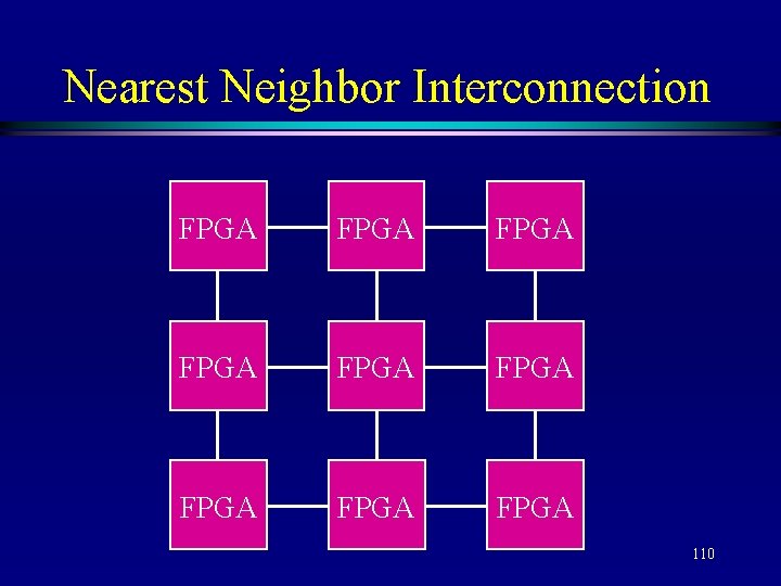
Nearest Neighbor Interconnection FPGA FPGA FPGA 110
Advantages and Disadvantages Advantages: - Uniform: all chips the same. Easy to lay out on PCB. l Disadvantages: - Routing is easily blocked. Through pins limit logic utilization of FPGAs. - Long and unpredictable delays. - No natural hierarchical extension. l - 111
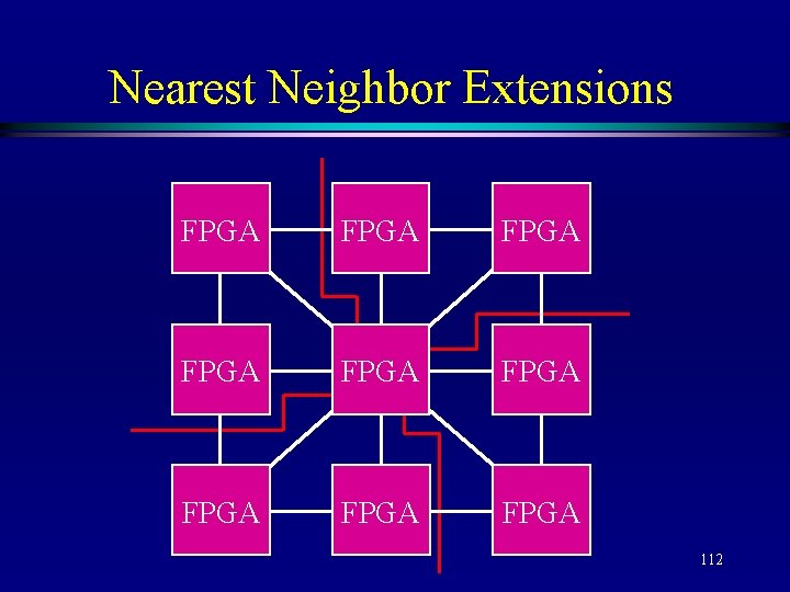
Nearest Neighbor Extensions FPGA FPGA FPGA 112
Advantages and Disadvantages Advantages: - More choices for router by adding diagonal lines & skip lines. l Disadvantages: - More complex PCB. - More complex routing software. l 113
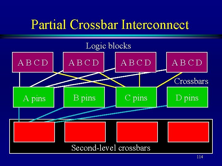
Partial Crossbar Interconnect Logic blocks ABCD Crossbars A pins B pins C pins D pins Second-level crossbars 114
Partial Crossbar Interconnect Partial crossbar consists of a set of small full crossbars, connected to logic blocks but not to each other. l I/O pins of each FPGA are divided into subsets. Each subset is connected by a full crossbar circuit switch. l Partial crossbar is a potentially blocking network. l 115
Partial Crossbar Characteristics Partial crossbar’s size is proportional to the number of FPGA pins. l All interconnections go through one/three crossbar chips for a one-level/two-level partial crossbar interconnect - delays are uniform and bounded. l 116
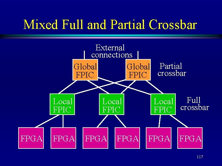
Mixed Full and Partial Crossbar External connections Global Partial FPIC crossbar Local FPIC FPGA Full Local FPIC crossbar FPGA 117
Circuit Switched Vs. Time Multiplexed Trade off operating speed and hardware cost. l Time-multiplexing method: - can greatly expand available interconnect. - allows lower cost IC package and PCB. - makes partitioning easier. BUT System power increases due to frequent signal switching (higher hardware cost). Complex scheduling software. Slow operating speed. 118 l
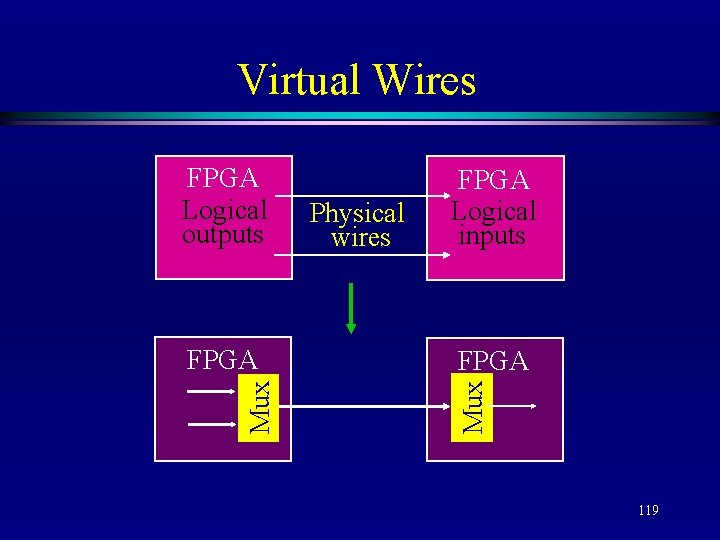
Virtual Wires Mux FPGA Physical wires FPGA Logical inputs FPGA Mux FPGA Logical outputs 119
Logic Emulation Systems System with mesh topology - Quickturn’s RPM and Virtual Machine Works (IKOS). l System with partial crossbar - Quickturn’s Enterprise, Mars, and System Realizer. l System with mixed full and partial crossbar Aptix Prototyping System. l System using time-multiplexed interconnect - Virtual Machine Works (IKOS) , Co. BALT and Arkos (Quickturn). l 120
Memory Solutions Goal: programmable memories with different width/depth/port combinations. l FPGA-based memories: - inefficient of using logic resources. - timing correctness is difficult to be insured. - large or highly multi-ported memories must be partitioned across several FPGAs. l SRAMs with dedicated or programmable controllers. l 121
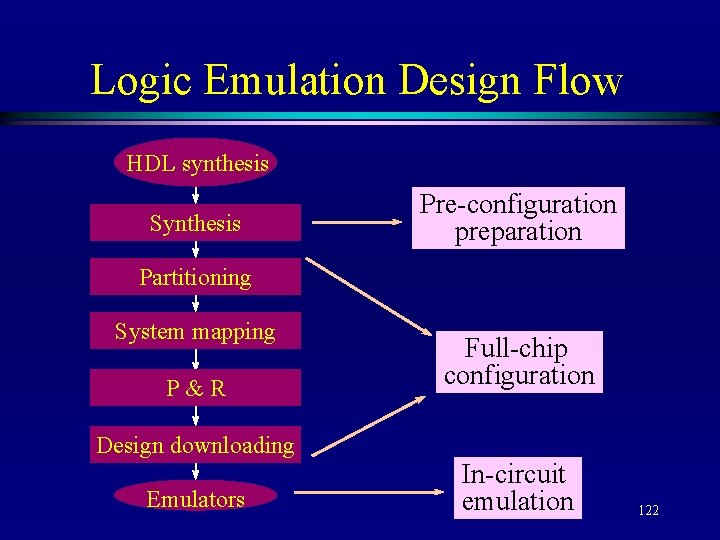
Logic Emulation Design Flow HDL synthesis Synthesis Pre-configuration preparation Partitioning System mapping P&R Design downloading Emulators Full-chip configuration In-circuit emulation 122
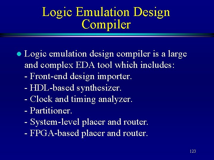
Logic Emulation Design Compiler l Logic emulation design compiler is a large and complex EDA tool which includes: - Front-end design importer. - HDL-based synthesizer. - Clock and timing analyzer. - Partitioner. - System-level placer and router. - FPGA-based placer and router. 123
Objectives Fast compilation time. l Fast emulation clock. l Timing correctness. l Easy ECO. l Minimize circuit size. l 124
Design Considerations HDL synthesis: - Trade-off run-time and quality. - CLB-based Vs. gate-based designs. l Clock and timing analysis: - Timing correctness, hold-time violation free. - Clock skew minimization. l Partitioning: - Run time. - Timing and area. l 125
Design Considerations System placement and routing: - Timing. - Completeness of routing. l FPGA-based placement and routing: - Fast run time. - Parallel compilation. l 126
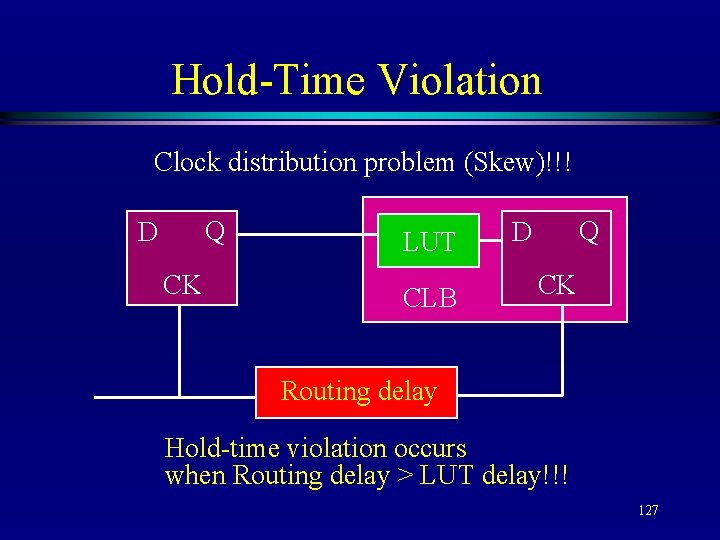
Hold-Time Violation Clock distribution problem (Skew)!!! Q D CK LUT CLB Q D CK Routing delay Hold-time violation occurs when Routing delay > LUT delay!!! 127
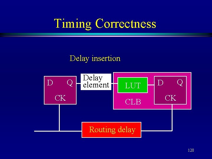
Timing Correctness Delay insertion Q D CK Delay element LUT CLB Q D CK Routing delay 128
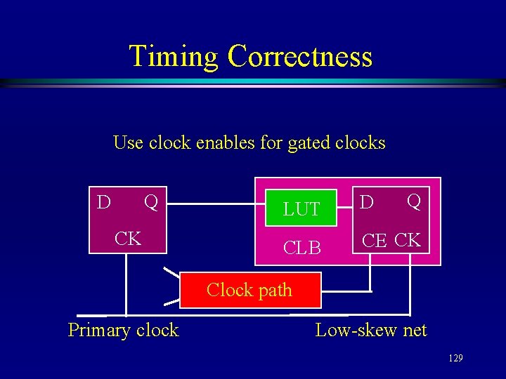
Timing Correctness Use clock enables for gated clocks Q D CK Q LUT D CLB CE CK Clock path Primary clock Low-skew net 129
Methodology Pre-configuration preparation - prepare netlists and control files for configuration. l Testbed preparation - prepare emulationbased operation environment. l Full-chip configuration - download design to the emulator. l In-circuit emulation - test the design. l 130
Pre-Configuration Translate the leaf-cell libraries into emulation primitives. l Translated libraries must be verified for functional equivalence to original. l Modify and redesign some components to attain compatibility with emulation techniques, such as precharge logic circuits. l Assemble all the gate-level netlists for the entire design. l 131
Testbed Design and implement target ICE board combining the emulated design with real hardware. l Slowdown testbed to emulation speed. l Assemble the testbed and emulation equipment. l 132
Full-Chip Configuration & In. Circuit Emulation Full-chip configuration: - Prepare control files. - Partition the design to fit into the emulation system. - Download design into the system. - Verify that emulation model faithfully implements the design as specified by RTL. l In-circuit emulation l 133
Part IV Reconfigurable Computing and Systems 134
General-Purpose Computing Vs. Custom Computing General-purpose computing - applying applications on a general-purpose computer. l Custom computing - applying applications on a custom-made application-specific hardware. l Field-programmable devices make this into a reality. l 135
Goals of Reconfigurable Computing Tailor the architecture to the application. l Minimize or eliminate instruction interpretation. l Exploit fine grained parallelism. l Map software to hardware. l 136
Applications Database search and analysis. l Image processing and machine vision. l Data compression. l Signal processing. l Neural networks. l Biology computing. l Medical computing. l Many more. l 137
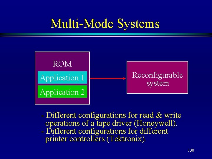
Multi-Mode Systems ROM Application 1 Application 2 Reconfigurable system - Different configurations for read & write operations of a tape driver (Honeywell). - Different configurations for different printer controllers (Tektronix). 138
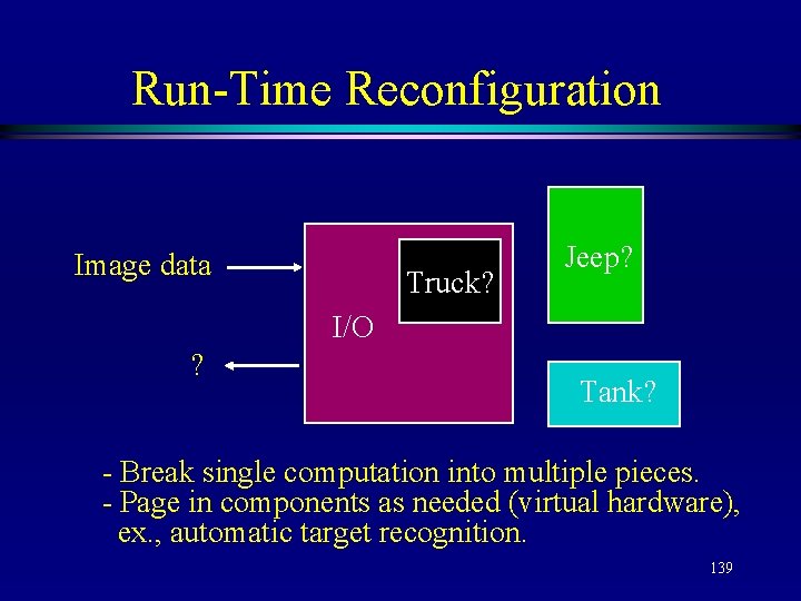
Run-Time Reconfiguration Image data Truck? Jeep? I/O ? Tank? - Break single computation into multiple pieces. - Page in components as needed (virtual hardware), ex. , automatic target recognition. 139
Custom Computing Application-specific systems. l Numerous applications for similar reconfigurable systems. l Offers hardware performance, flexibility to handle numerous algorithms. l Multi-FPGA systems can be viewed as hardware supercomputers. l 140
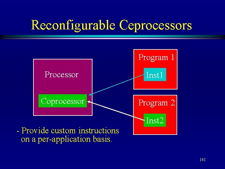
Reconfigurable Ceprocessors Program 1 Processor Inst 1 Coprocessor Program 2 Inst 2 - Provide custom instructions on a per-application basis. 141
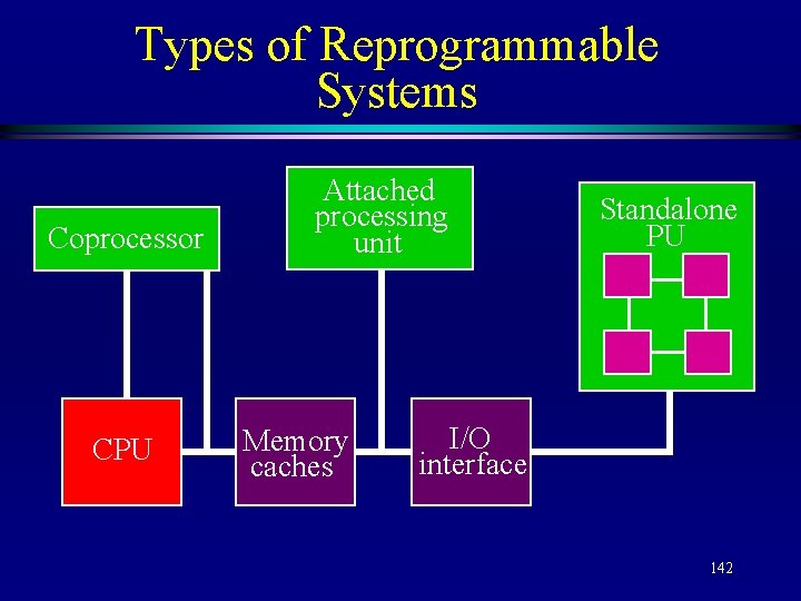
Types of Reprogrammable Systems Coprocessor CPU Attached processing unit Memory caches Standalone PU I/O interface 142
Types of Reprogrammable Systems Attached and standalone processing units are reprogrammable systems on computer addon cards and separate reprogrammable cabinets. Considerations: large communication overhead may over-shadow the speed gain. l Application-specific coprocessors can achieve significant improvement over a wide range of applications. l 143
Types of Reprogrammable Systems l Integrate the reprogrammable logic into the processor itself. - A reprogrammable functional unit can be configured on a per-algorithm basis. - Providing some special-purpose instructions tailored to the needs of a given application. 144
Architectures of Multi-FPGA Systems l The most commonly used topologies: - Mesh: 1 D (linear array), 2 D, and 3 D. - Crossbar: full, partial, mixed, and hierarchical. - Hybrid between mesh and crossbar. - Application-specific architecture. 145
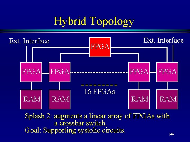
Hybrid Topology Ext. Interface FPGA RAM 16 FPGAs Ext. Interface FPGA RAM Splash 2: augments a linear array of FPGAs with a crossbar switch. Goal: Supporting systolic circuits. 146
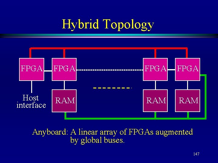
Hybrid Topology FPGA Host interface RAM RAM Anyboard: A linear array of FPGAs augmented by global buses. 147
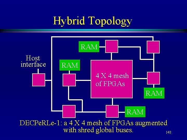
Hybrid Topology RAM Host interface RAM 4 X 4 mesh of FPGAs RAM DECPe. RLe-1: a 4 X 4 mesh of FPGAs augmented with shred global buses. 148
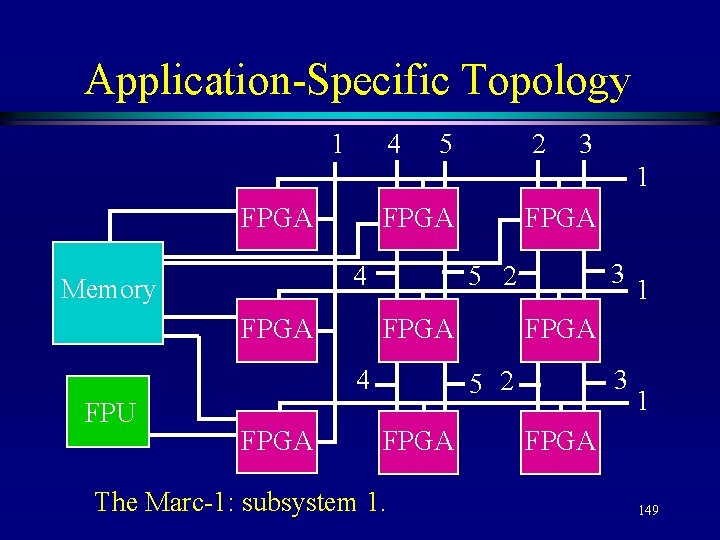
Application-Specific Topology 4 1 5 2 3 1 FPGA 4 Memory FPGA 3 5 2 FPGA 4 FPU FPGA 3 5 2 FPGA The Marc-1: subsystem 1. 1 1 FPGA 149
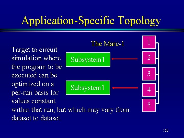
Application-Specific Topology The Marc-1 Target to circuit simulation where Subsystem 1 the program to be executed can be optimized on a Subsystem 1 per-run basis for values constant within that run, but which may vary from dataset to dataset. 1 2 3 4 5 150
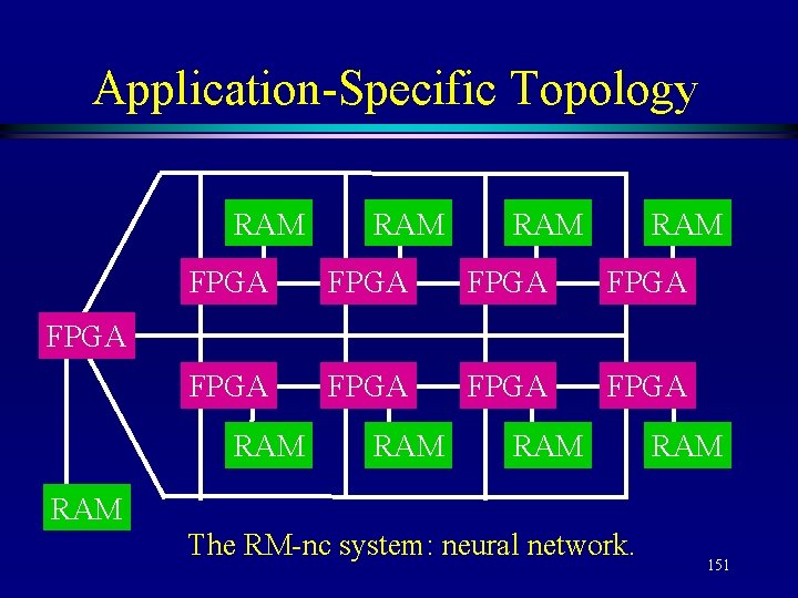
Application-Specific Topology RAM RAM FPGA FPGA FPGA RAM RAM RAM The RM-nc system: neural network. 151
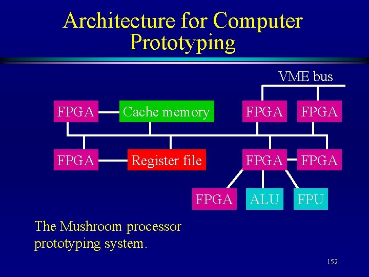
Architecture for Computer Prototyping VME bus FPGA Cache memory FPGA Register file FPGA ALU FPGA The Mushroom processor prototyping system. 152
Expandable Topology Hierarchical crossbar topology: by adding extra level. Quickturn systems. l Expandable mesh topology: by connecting individual board to form a large mesh. - The Virtual Wires Emulation System (IKOS). l 153
Topology for Adapting Other Components Many multi-FPGA systems include non. FPGA resources to provide more general purpose solutions. l The MORRPH system - sockets next to FPGAs which allow to add arbitrary devices to the array. l The G 800 board - contains two FPGAs and four sockets. l 154
Topology for Adapting Other Components The COBRA system - contains based modules (expanding to 2 D mesh), RAM modules, I/O modules, and bus modules. l The Springbok system - pre-made daughter board which is able to contain an arbitrary device (on the top) and an FPGA (on the bottom). Daughter boards is mounted on a baseplate. l 155
Topology for Adapting Other Components The Quickturn systems - external component adapters. l The Aptix FPCB - a reprogrammable PCB. l 156
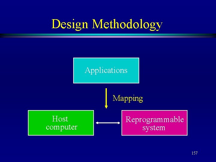
Design Methodology Applications Mapping Host computer Reprogrammable system 157
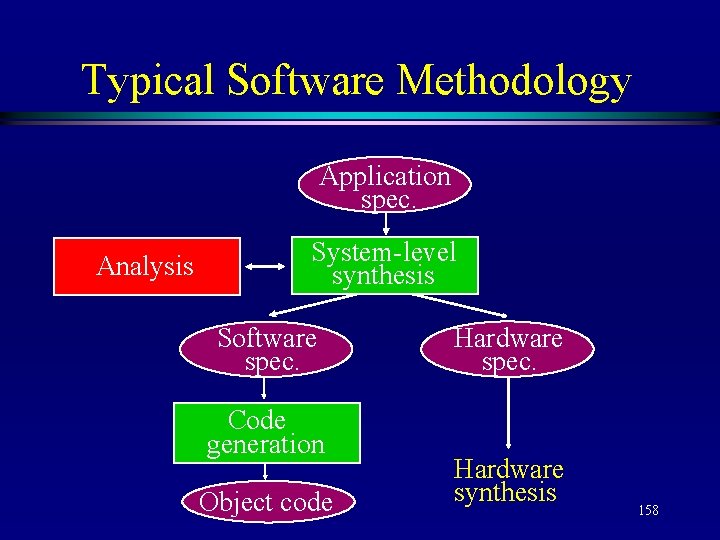
Typical Software Methodology Application spec. Analysis System-level synthesis Software spec. Code generation Object code Hardware spec. Hardware synthesis 158
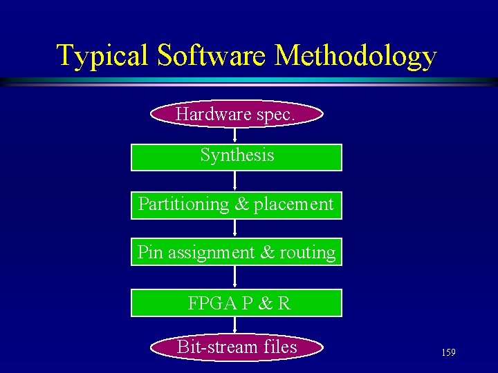
Typical Software Methodology Hardware spec. Synthesis Partitioning & placement Pin assignment & routing FPGA P & R Bit-stream files 159
Considerations Architectural-specific design tasks. l Design automation process. l The mapping time dominates the setup time for operating the system. l Run-time reconfigurability. l 160
Design Specification and Languages Standard software programming languages, e. g. , C, C++, FORTRAN, and assembly language, Vs. HDLs. l Standard software programming languages a sequential execution model. l HDLs - a parallel execution model. l Who will use it and which one is more suitable for system description? ? ? l 161
Compilation Issues Translate code from software languages into hardware without losing the inherent concurrency of hardware. l Compiler techniques for parallelizing code. l Straight-line code, control flow, and loops. l Transmogrifier C compiler. l 162
System-level and High-level Synthesis System-level design evaluation and analysis. l Design estimation. l Hardware-software partitioning. l Interface synthesis. l RTL synthesis. l Logic synthesis and technology mapping. l 163
Partitioning and Placement Topology-aware partitioning methods. l Partitioning onto a multi-FPGA system is equivalent to a placement problem. l Logic utilization and timing. l 164
Pin Assignment and Routing Pin-assignment - the process of determining which I/O pins to be used for each inter. FPGA signal. l Pin-assignment for a pre-fabricated multi. FPGA system is equivalent to the global routing problem. l Pin-assignment will greatly affect the quality of FPGA’s logic utilization and routability. l 165
Run-Time Reconfigurability Virtual hardware <=> virtual memory. l Hardware on demand. l Unconfigured and reconfiguring methods. l Software supporting time-varying mapping. l Many open problems need to be solved in the forth coming years. l 166
Applications: Splash 2 Stream oriented systolic and SIMD applications. l Scalable linear array of 16 to 256 processing elements (1 XC 4010 with 1/2 Mbyte). l VHDL based. l Sequence comparison - 2300 M: 0. 75 M cell updates/sec (Splash 2: Sparc 10). l Edge detection - 10 M: 242 K pixels/sec (Splash 2: Sparc 10). l 167
Applications: PAM (DEC) Programmable Active Memory (PAM). l C++ based and mesh arrays of XC 3090 (DECPe. RLe-1). l Applications: - Multiple precision arithmetic. - RSA encryption. - Video compression (JPEG, MPEG, DCT). - High energy physics. - Telecommunications. l 168
- Slides: 168