Range Enhanced Packet Classification Design on FPGA Author

- Slides: 29

Range Enhanced Packet Classification Design on FPGA Author: Yeim-Kuan Chang, Chun-sheng Hsueh Publisher: IEEE Transactions on Emerging Topics in Computing Presenter: Yi-Hao Lai Date: 2015/11/25 Department of Computer Science and Information Engineering National Cheng Kung University, Taiwan R. O. C.

Introduction l Two schemes to process range fields • The first scheme has the same characteristic as • Stride. BV by using specially designed codes to store the precomputed results in memory. The second scheme uses a simple subrange comparison method to find the matching result in a sequential fashion. National Cheng Kung University CSIE Computer & Internet Architecture Lab 2

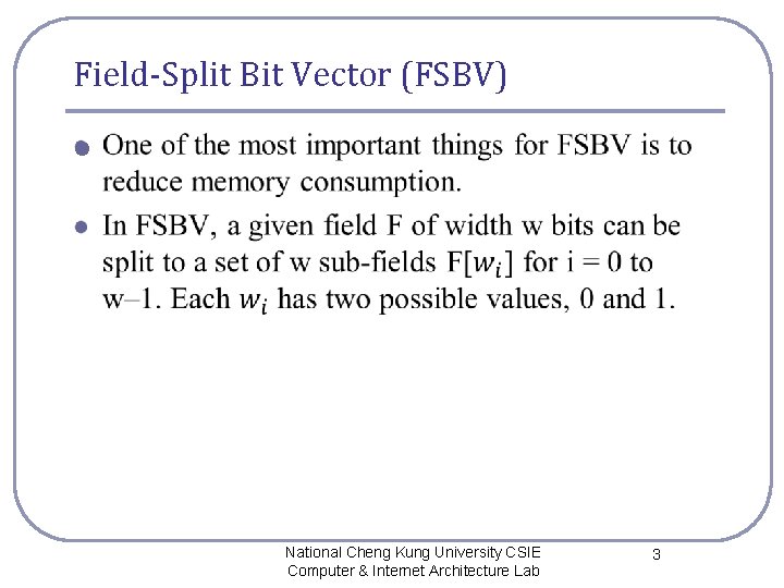
Field-Split Bit Vector (FSBV) l National Cheng Kung University CSIE Computer & Internet Architecture Lab 3

Field-Split Bit Vector (FSBV) National Cheng Kung University CSIE Computer & Internet Architecture Lab 4

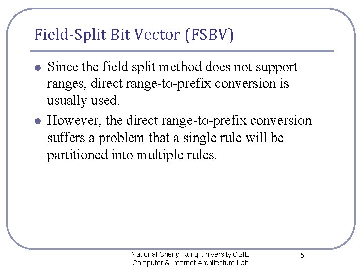
Field-Split Bit Vector (FSBV) l l Since the field split method does not support ranges, direct range-to-prefix conversion is usually used. However, the direct range-to-prefix conversion suffers a problem that a single rule will be partitioned into multiple rules. National Cheng Kung University CSIE Computer & Internet Architecture Lab 5

Stride Bit Vector (Stride. BV) l National Cheng Kung University CSIE Computer & Internet Architecture Lab 7

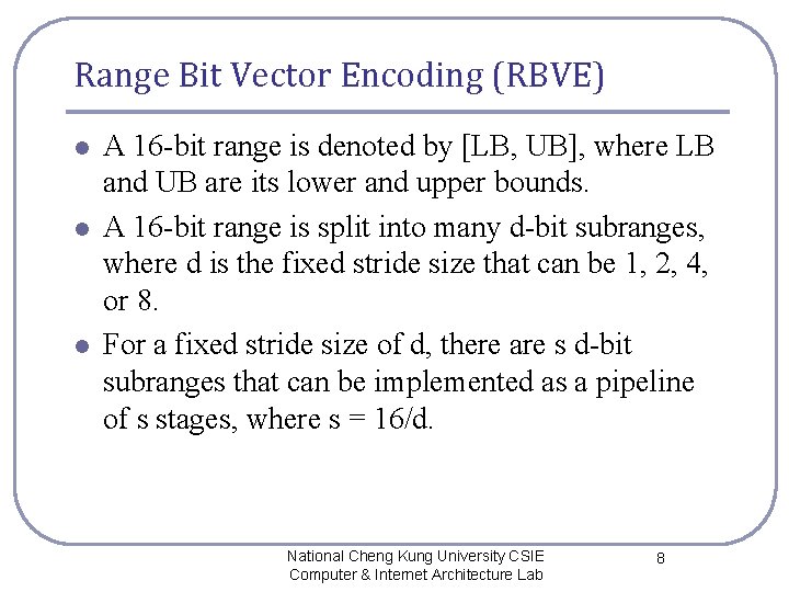
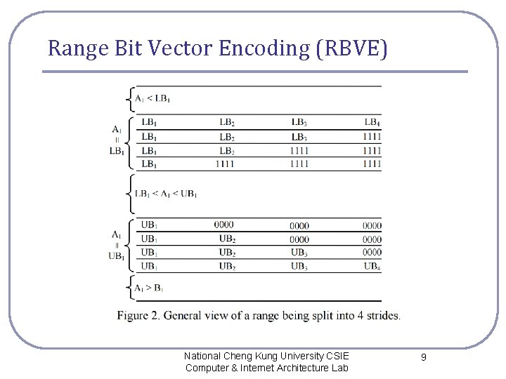
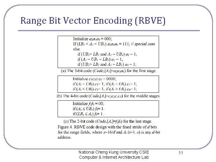
Range Bit Vector Encoding (RBVE) l l l A 16 -bit range is denoted by [LB, UB], where LB and UB are its lower and upper bounds. A 16 -bit range is split into many d-bit subranges, where d is the fixed stride size that can be 1, 2, 4, or 8. For a fixed stride size of d, there are s d-bit subranges that can be implemented as a pipeline of s stages, where s = 16/d. National Cheng Kung University CSIE Computer & Internet Architecture Lab 8

Range Bit Vector Encoding (RBVE) National Cheng Kung University CSIE Computer & Internet Architecture Lab 9

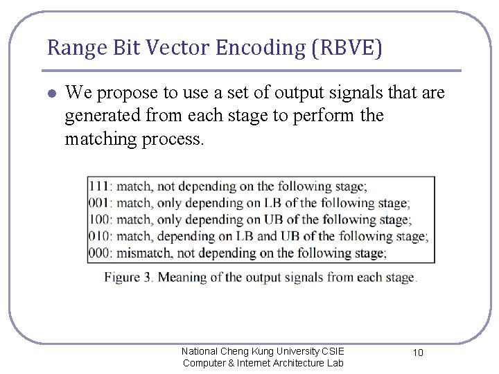
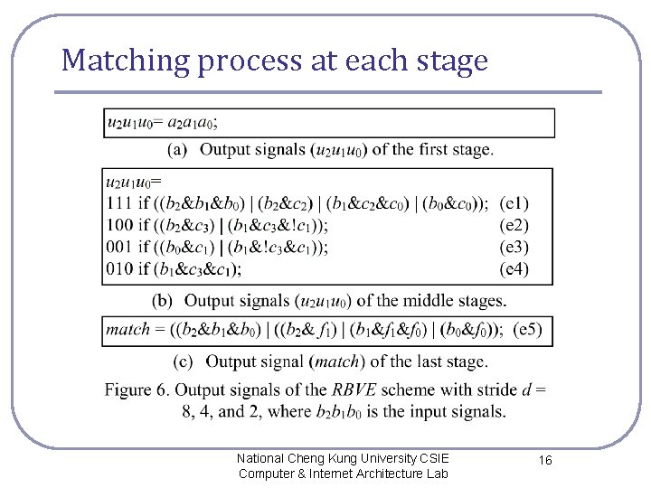
Range Bit Vector Encoding (RBVE) l We propose to use a set of output signals that are generated from each stage to perform the matching process. National Cheng Kung University CSIE Computer & Internet Architecture Lab 10

Range Bit Vector Encoding (RBVE) National Cheng Kung University CSIE Computer & Internet Architecture Lab 11

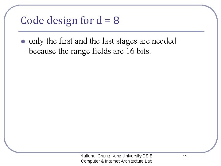
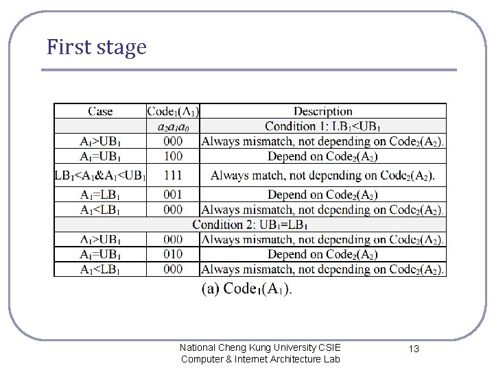
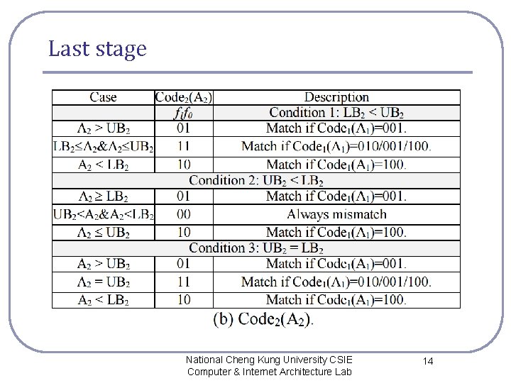
Code design for d = 8 l only the first and the last stages are needed because the range fields are 16 bits. National Cheng Kung University CSIE Computer & Internet Architecture Lab 12

First stage National Cheng Kung University CSIE Computer & Internet Architecture Lab 13

Last stage National Cheng Kung University CSIE Computer & Internet Architecture Lab 14

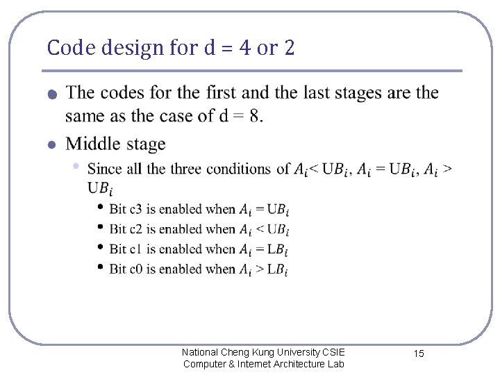
Code design for d = 4 or 2 l National Cheng Kung University CSIE Computer & Internet Architecture Lab 15

Matching process at each stage National Cheng Kung University CSIE Computer & Internet Architecture Lab 16

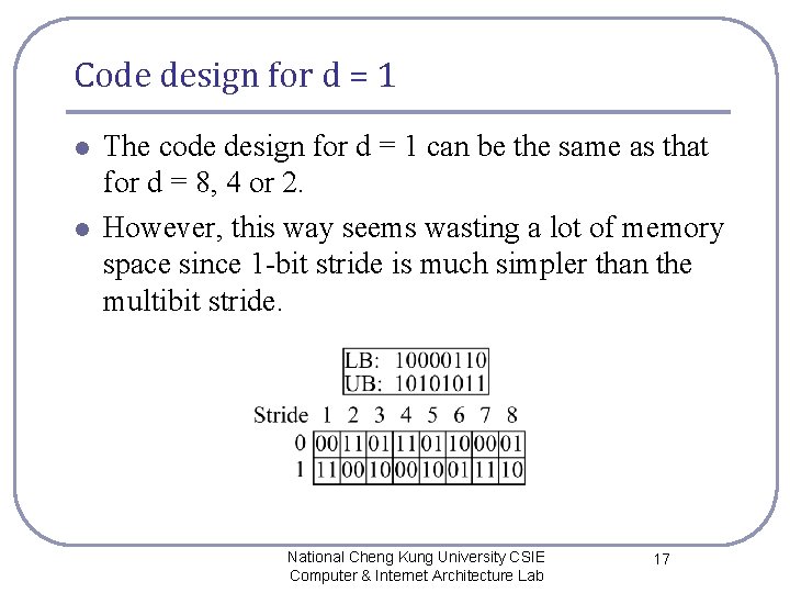
Code design for d = 1 l l The code design for d = 1 can be the same as that for d = 8, 4 or 2. However, this way seems wasting a lot of memory space since 1 -bit stride is much simpler than the multibit stride. National Cheng Kung University CSIE Computer & Internet Architecture Lab 17

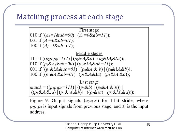
Matching process at each stage National Cheng Kung University CSIE Computer & Internet Architecture Lab 18

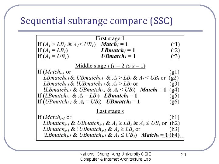
Sequential subrange compare (SSC) l l l stores subranges directly in the memory and performs subrange match operations sequentially. The subranges split from a range are classified into three types, the first, the middle, and the last subranges. we need four types of matching results that are represented by the signals, Match, Mismatch, LBmatch, and UBmatch. National Cheng Kung University CSIE Computer & Internet Architecture Lab 19

Sequential subrange compare (SSC) National Cheng Kung University CSIE Computer & Internet Architecture Lab 20

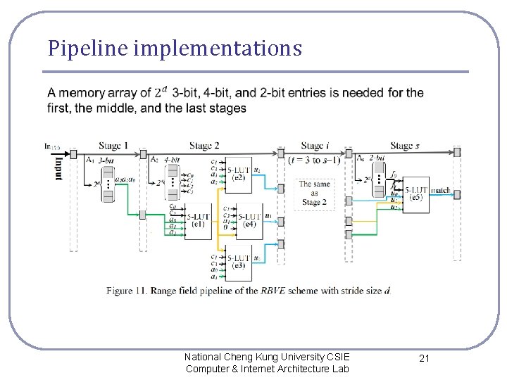
Pipeline implementations National Cheng Kung University CSIE Computer & Internet Architecture Lab 21

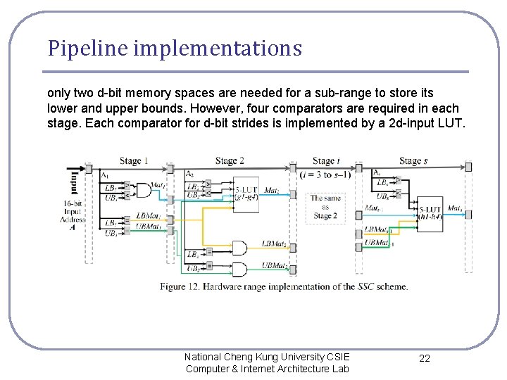
Pipeline implementations only two d-bit memory spaces are needed for a sub-range to store its lower and upper bounds. However, four comparators are required in each stage. Each comparator for d-bit strides is implemented by a 2 d-input LUT. National Cheng Kung University CSIE Computer & Internet Architecture Lab 22

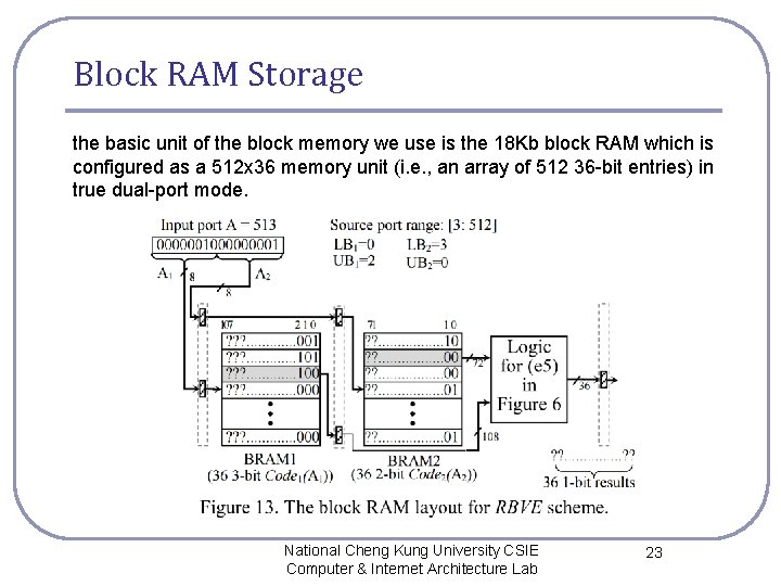
Block RAM Storage the basic unit of the block memory we use is the 18 Kb block RAM which is configured as a 512 x 36 memory unit (i. e. , an array of 512 36 -bit entries) in true dual-port mode. National Cheng Kung University CSIE Computer & Internet Architecture Lab 23

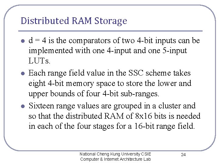
Distributed RAM Storage l l l d = 4 is the comparators of two 4 -bit inputs can be implemented with one 4 -input and one 5 -input LUTs. Each range field value in the SSC scheme takes eight 4 -bit memory space to store the lower and upper bounds of four 4 -bit sub-ranges. Sixteen range values are grouped in a cluster and so that the distributed RAM of 8 x 16 bits is needed in each of the four stages for a 16 -bit range field. National Cheng Kung University CSIE Computer & Internet Architecture Lab 24

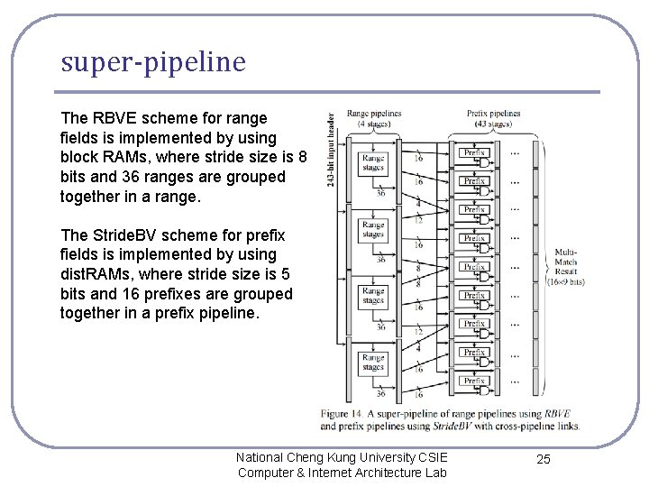
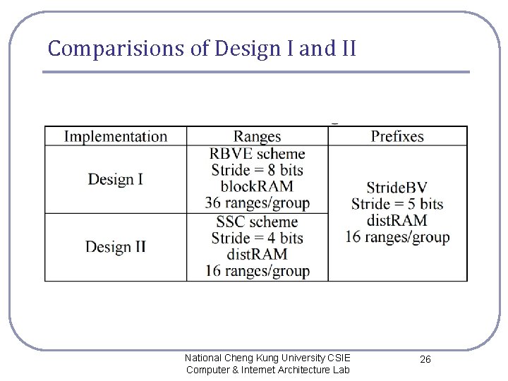
super-pipeline The RBVE scheme for range fields is implemented by using block RAMs, where stride size is 8 bits and 36 ranges are grouped together in a range. The Stride. BV scheme for prefix fields is implemented by using dist. RAMs, where stride size is 5 bits and 16 prefixes are grouped together in a prefix pipeline. National Cheng Kung University CSIE Computer & Internet Architecture Lab 25

Comparisions of Design I and II National Cheng Kung University CSIE Computer & Internet Architecture Lab 26

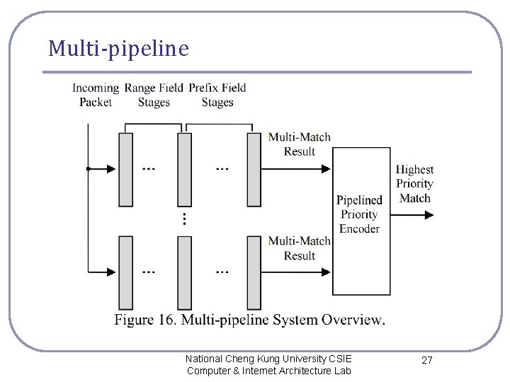
Multi-pipeline National Cheng Kung University CSIE Computer & Internet Architecture Lab 27

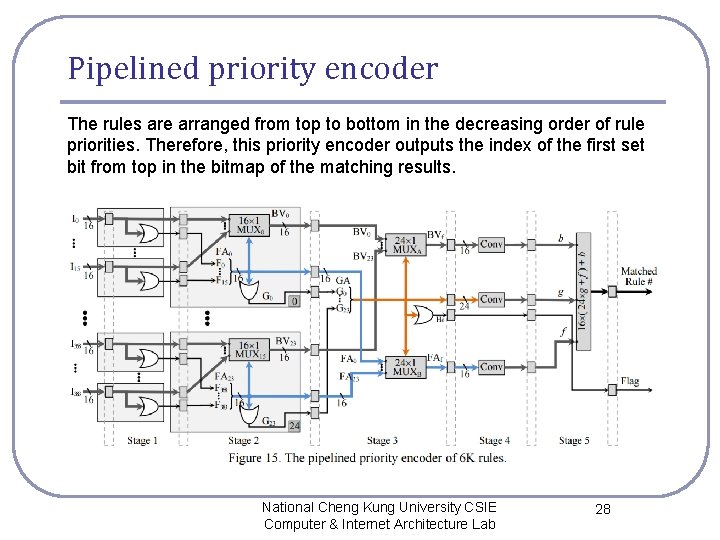
Pipelined priority encoder The rules are arranged from top to bottom in the decreasing order of rule priorities. Therefore, this priority encoder outputs the index of the first set bit from top in the bitmap of the matching results. National Cheng Kung University CSIE Computer & Internet Architecture Lab 28

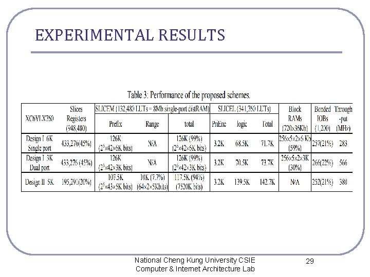
EXPERIMENTAL RESULTS National Cheng Kung University CSIE Computer & Internet Architecture Lab 29

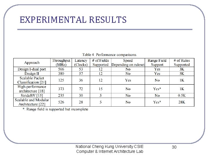
EXPERIMENTAL RESULTS National Cheng Kung University CSIE Computer & Internet Architecture Lab 30