Random Number Generator March 1 2006 Component Layout

Random Number Generator March 1, 2006 Component Layout and Floorplan Layout Count: 14, 300 Dmitriy Solmonov W 1 -1 David Levitt W 1 -2 Jesse Guss W 1 -3 Sirisha Pillalamarri W 1 -4 Matt Russo W 1 -5 Design Manager – Thiago Hersan Project Objective: Create a Cryptologically Secure Pseudo-Random Number Generator

Agenda • • • Status Design Decisions Verification & Simulation Review DFM & Layout Rules Critical Layouts Floorplan & Design Specs

Status Former ü C implementation ü Architecture ü Behavioral Design and Simulation ü Gate-Level Design and Simulation ü Preliminary Floorplan ü Schematic Design and Simulation Currently Ø Layout (14, 300 of 34, 710) Awaiting • Extraction, LVS, post-layout simulation

Design Decisions • Registers Re-designed – All registers based on n-pass DFF – Reduce size, power, complexity • Reduction in instances of gates & inverters t-

DFF w/ Synchronous Load & CLR

Register Comparisons Type Transistors Power DFF 18 10µW HLFF 26 60µW

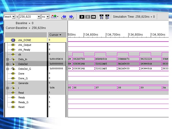
Verification • Tested structural verilog against C code for correct result. • Tested verilog schematic against structural verilog for matching signals • Performed spectre analysis of key modules

DFM & ME • The Rules – Everything is on a grid – Everything is mono-directional – All metal widths are the same – Contacts same width as metals

Pros • • Regular Layout Enforced Standardization More Accurate Resolution Contacts match metal widths

Example: Group Propagate

CONS • • • Harder to “cut-corners” More time-involving Increased Area Decreased Speed More Metal Layers Learning Curve

Minimize Inverter Use • DFM rules make inverters the more wasteful than any other gate • No good way to make them, either waste area or avoid inverters

MUX’s • Inefficient • No routing through it • BIG

Completed Layouts: 3 Bit Adder Block

3 Bit Adder Block

SRAM Single Bus Cell Double Bus Cell
")
SRAM (R)
")
SRAM (M)

Updated Floorplan
 Component Transistor Count Area Prop Delay Power")
Putting it All Together (Updated power calculations) Component Transistor Count Area Prop Delay Power Adders (4 x) 5856 (1464 each) 2700 um 2 (675 um 2 ea. ) 1. 44 ns 575 u. W FSM 194 100 um 2 826 ps 46 u. W SRAM 17736 (M=10458 R=7278) 8000 um 2 735 ps W: 510 u. W R: 190 u. W Datapath w/o Adders 10924 5000 um 2 Total 34710 15800 um 2 3. 3 m. W 500 MHz ~6. 5 m. W
")
Thanks! Any Questions? (Beware the Cadence Ninja)
- Slides: 22