Random Number Generator March 1 2006 Component Layout

Random Number Generator March 1, 2006 Component Layout and Floorplan Dmitriy Solmonov W 1 -1 David Levitt W 1 -2 Jesse Guss W 1 -3 Sirisha Pillalamarri W 1 -4 Matt Russo W 1 -5 Design Manager – Thiago Hersan Project Objective: Create a Cryptologically Secure Pseudo-Random Number Generator

Need for Encryption • Explain how a good random number can make data transfer that much more secure.

Random Number? • Pseudo-random number generator • Uses RC 4 encryption algorithm – Cryptographically secure • Internally Updated Seed – not in programmer's visible state – hacker

Usage

Demand • Potential markets – Defense and Intelligence Organizations – Gambling – Component of future secure mobile communications
 #define SIZE (1<<ALPHA) #define ind(x) ((x)&(0 x 1")
The IBAA Algorithm #define ALPHA (8) #define SIZE (1<<ALPHA) #define ind(x) ((x)&(0 x 1 F)) #define barrel(a) (((a)<<19)^((a)13)) /*beta=32, shift=19*/ … y=y 1+b; m[ind(i)]=y; b=m[ind(y>>ALPHA]+x; r[ind(i)]=b; for(i=0; i<SIZE; ++i){ X=m[ind(i)]; A=barrel(a)+m[ind(I +16)]; Y 1=m[ind(x)]+a; Y=y 1+b; M[ind(i)]=y; B=m[ind(y)>>ALPHA]+x; R[ind(i)]=b; }

Algorithm Animation • TBC

Algorithm to Architecture • Explain progression from C code to choice of hardware.

Algorithm to Architecture • Explain the choice for a 2 -Stage Pipeline with multiple cycles per stage.

Algorithm to Architecture • Explain why 4 cycles per stage yields the best throughput under hardware assumptions

typedef unsigned int u 4; /* unsigned four bytes, 32 bits */ #define ALPHA (8) #define SIZE (1<<ALPHA) #define ind(x) ((x)&(SIZE-1)) (X) (M 4) (M 1, M 2, M 3) Registers SRAM (M) Adder Reg #define barrel(a) (((a)<<19)^((a)>>13)) /* beta=32, shift=19 */ static void ibaa(m, r, aa, bb) u 4 *m; /* Memory: array of SIZE ALPHA-bit terms */ u 4 *r; /* Results: the sequence, same size as m */ u 4 *aa; /* Accumulator: a single value */ u 4 *bb; /* the previous result */ Control Logic FSM Counter Register { register u 4 a, b, x, y, i; a = *aa; b = *bb; for (i=0; i<SIZE; ++i) { x = m[i]; SRAM (R) a = barrel(a) + m[ind(i+(SIZE/2))]; /* set a */ (B) Reg (Y) Reg Adder (Y 1) Reg Adder (A) Reg Adder m[i] = y = m[ind(x)] + a + b; /* set m */ r[i] = b = m[ind(y>>ALPHA)] + x; /* set r */ } *bb = b; *aa = a; }

Floorplan Evolution: #1

Floorplan #2

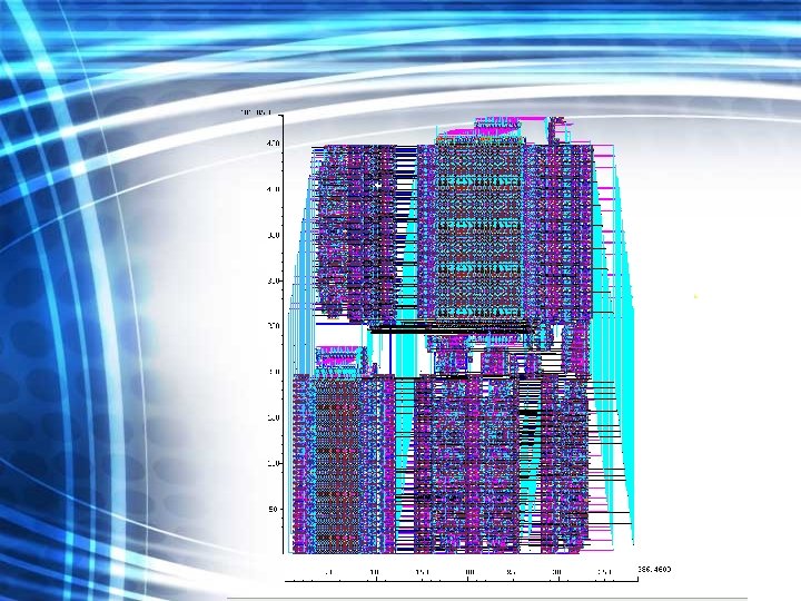
Final Floorplan

• Animation showing what happens on every cycle of the loop.

DFM & ME • The Rules – Everything is on a grid – Everything is mono-directional – All metal widths are the same – Contacts same width as metals

Why DFM • Easier to perform RET • Manufacturability • A must for the new generation of transistor sizes.

Pros • • Regular Layout Enforced Standardization More Accurate Resolution Contacts match metal widths

Example: Group Propagate

CONS • • • Harder to “cut-corners” More time-involving Increased Area Decreased Speed More Metal Layers Learning Curve

Adder • Four adders execute 256 times each to generate one number. • Hybrid carry skip, carry look ahead, conditional sum, … • Fast and low power. • Chirca, Schulte, Glossner, et al. “A Static Low-Power, High-Performance 32 bit Carry Skip Adder” http: //mesa. ece. wisc. edu/publications/cp_2004 -12. pdf
![C[32] CS 4 S[31: 28] C’[28] CS 18 S[27: 10] C[10] CS 6 S[9:](http://slidetodoc.com/presentation_image_h2/0354e31fb0ba3263bdea22be906e20f6/image-22.jpg "C[32] CS 4 S[31: 28] C’[28] CS 18 S[27: 10] C[10] CS 6 S[9:")
C[32] CS 4 S[31: 28] C’[28] CS 18 S[27: 10] C[10] CS 6 S[9: 4] C’[4] CS 4 S[3: 0] C[0] A[3: 0] B[3: 0] A[9: 4] B[9: 4] A[27: 10] B[27: 10] A[31: 28] B[31: 28] 32 -Bit Adder Block Diagram

32 -Bit Adder First CS 4 Block

32 -Bit Adder CS 18 Block

32 Bit Fast Adder

Adder Performance • Discuss trade off’s in speed and power.

SRAM Single Bus Cell Double Bus Cell

SRAM Single Bus

Dual Bus SRAM

Discuss Speed and Power • SRAM power consumption • Why we can’t do better with the SRAM

Verification • Tested architectural verilog against C code for matching 1024 -bit number results. • Tested architectural verilog against structural verilog for matching port outputs.

Verification • Verified Schematic against Verilog implementation in cadence – Made sure that output was the same – Checked delays and voltage levels • Verified layout vs. schematic – Checked levels with parasitics – Performed LVS test

Poly Density 7. 06%

Metal Density 19. 59 %

Metal 2 Density 18. 85%

Metal 3 Density 19. 24%

Metal 4 Density 8. 91% Metal 5 Density 4. 75%

Critical Delay
 – 32 output")
Specs • Pins – 40 input pins (including clock, vdd, gnd) – 32 output pins (the random number) • 475 MHz chip speed • 436 KHz throughput
 Registers (10) Power (Average)")
Putting it All Together Trans Count Prop Delay SRAM (M&R) Registers (10) Power (Average) @ 500 MHz 1. 45 ns 1. 56 ns 600 u. W 620 u. W 148 u. W 270 u. W 1. 86 m. W Schematic #s Extract. RC #s Area Density 5, 856 (1, 464 ea. ) 25, 200 um 2 (6, 300 um 2 ea. ) 0. 232 17, 736 (M=10, 458 R=7, 278) 51, 000 um 2 (M=35, 000 R=16, 000 0. 348 (M=0. 293 R=0. 456) 735 ps 845 ps W: 510 u. W W: 3. 25 m. W R: 190 u. W R: 1. 40 m. W 6400 (640 ea. ) 38, 400 um 2 (3, 840 um 2 ea. ) 0. 167 220 ps 275 ps 530 u. W 590 u. W 182, 000 um 2 0. 183 Part Adders (4) Power (1 x) @ 500 MHz Total 33225 2. 1 ns 475 MHz ----- 130 u. W 145 u. W 4. 1 m. W

Questions
- Slides: 42