Radiationhardenedbydesign RHBD Preamplifier design for Radiation Harsh Environment

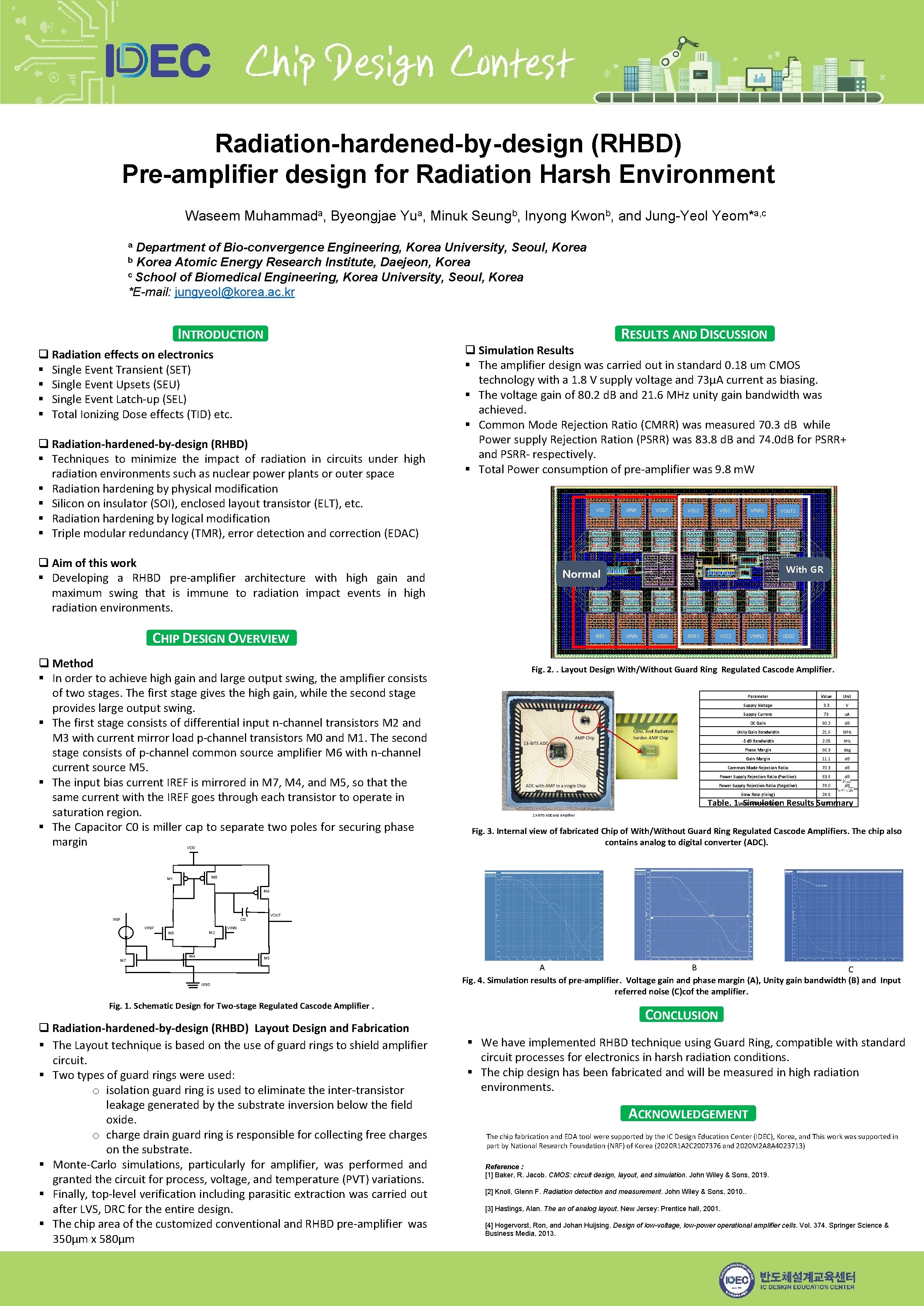
Radiation-hardened-by-design (RHBD) Pre-amplifier design for Radiation Harsh Environment Waseem Muhammada, Byeongjae Yua, Minuk Seungb, Inyong Kwonb, and Jung-Yeol Yeom*a, c Department of Bio-convergence Engineering, Korea University, Seoul, Korea b Korea Atomic Energy Research Institute, Daejeon, Korea c School of Biomedical Engineering, Korea University, Seoul, Korea *E-mail: jungyeol@korea. ac. kr a RESULTS AND DISCUSSION INTRODUCTION q Radiation effects on electronics § Single Event Transient (SET) § Single Event Upsets (SEU) § Single Event Latch-up (SEL) § Total Ionizing Dose effects (TID) etc. q Radiation-hardened-by-design (RHBD) § Techniques to minimize the impact of radiation in circuits under high radiation environments such as nuclear power plants or outer space § Radiation hardening by physical modification § Silicon on insulator (SOI), enclosed layout transistor (ELT), etc. § Radiation hardening by logical modification § Triple modular redundancy (TMR), error detection and correction (EDAC) q Aim of this work § Developing a RHBD pre-amplifier architecture with high gain and maximum swing that is immune to radiation impact events in high radiation environments. q Simulation Results § The amplifier design was carried out in standard 0. 18 um CMOS technology with a 1. 8 V supply voltage and 73μA current as biasing. § The voltage gain of 80. 2 d. B and 21. 6 MHz unity gain bandwidth was achieved. § Common Mode Rejection Ratio (CMRR) was measured 70. 3 d. B while Power supply Rejection Ration (PSRR) was 83. 8 d. B and 74. 0 d. B for PSRR+ and PSRR- respectively. § Total Power consumption of pre-amplifier was 9. 8 m. W VSS VDD VOUT VSS 2 VINP 2 IREF VOUT 2 With GR Normal CHIP DESIGN OVERVIEW q Method § In order to achieve high gain and large output swing, the amplifier consists of two stages. The first stage gives the high gain, while the second stage provides large output swing. § The first stage consists of differential input n-channel transistors M 2 and M 3 with current mirror load p-channel transistors M 0 and M 1. The second stage consists of p-channel common source amplifier M 6 with n-channel current source M 5. § The input bias current IREF is mirrored in M 7, M 4, and M 5, so that the same current with the IREF goes through each transistor to operate in saturation region. § The Capacitor C 0 is miller cap to separate two poles for securing phase margin VINP VINN VDD IREF 2 VINN 2 VSS 2 VDD 2 Fig. 2. . Layout Design With/Without Guard Ring Regulated Cascode Amplifier. Parameter Value Unit Supply Voltage 3. 3 V Supply Current 73 u. A DC Gain 80. 2 d. B Unity Gain Bandwidth 21. 6 MHz -3 d. B Bandwidth 2. 05 k. Hz Phase Margin 66. 3 deg Gain Margin 11. 1 d. B Common Mode Rejection Ratio 70. 3 d. B Power Supply Rejection Ratio (Positive) 83. 8 d. B Power Supply Rejection Ratio (Negative) 74. 0 d. B Slew Rate (rising) 24. 8 Referred Noise 1. 99 Table. 1. Input Simulation Results Summary 13 -BITS ADC and Amplifier Fig. 3. Internal view of fabricated Chip of With/Without Guard Ring Regulated Cascode Amplifiers. The chip also contains analog to digital converter (ADC). M 0 M 1 M 6 IREF VINP M 2 M 3 M 7 VOUT C 0 M 4 VINN M 5 GND Fig. 1. Schematic Design for Two-stage Regulated Cascode Amplifier. q Radiation-hardened-by-design (RHBD) Layout Design and Fabrication § The Layout technique is based on the use of guard rings to shield amplifier circuit. § Two types of guard rings were used: o isolation guard ring is used to eliminate the inter-transistor leakage generated by the substrate inversion below the field oxide. o charge drain guard ring is responsible for collecting free charges on the substrate. § Monte-Carlo simulations, particularly for amplifier, was performed and granted the circuit for process, voltage, and temperature (PVT) variations. § Finally, top-level verification including parasitic extraction was carried out after LVS, DRC for the entire design. § The chip area of the customized conventional and RHBD pre-amplifier was 350μm x 580μm A B C Fig. 4. Simulation results of pre-amplifier. Voltage gain and phase margin (A), Unity gain bandwidth (B) and Input referred noise (C)cof the amplifier. CONCLUSION § We have implemented RHBD technique using Guard Ring, compatible with standard circuit processes for electronics in harsh radiation conditions. § The chip design has been fabricated and will be measured in high radiation environments. ACKNOWLEDGEMENT The chip fabrication and EDA tool were supported by the IC Design Education Center (IDEC), Korea, and This work was supported in part by National Research Foundation (NRF) of Korea (2020 R 1 A 2 C 2007376 and 2020 M 2 A 8 A 4023713) Reference : [1] Baker, R. Jacob. CMOS: circuit design, layout, and simulation. John Wiley & Sons, 2019. [2] Knoll, Glenn F. Radiation detection and measurement. John Wiley & Sons, 2010. . [3] Hastings, Alan. The an of analog layout. New Jersey: Prentice hall, 2001. [4] Hogervorst, Ron, and Johan Huijsing. Design of low-voltage, low-power operational amplifier cells. Vol. 374. Springer Science & Business Media, 2013.
- Slides: 1