Radiation Tolerant Intelligent Memory Stack RTIMS Takkwong Ng
- Slides: 27

Radiation Tolerant Intelligent Memory Stack (RTIMS) Tak-kwong Ng, Jeffrey Herath Electronics Systems Branch Systems Engineering Directorate NASA Langley Research Center t. ng@nasa. gov jeffrey. a. herath@nasa. gov 757 -864 -1097 (Tak) 757 -864 -1098 (Jeff) Ng La. RC 1 MAPLD 2005 / A 208

Agenda • • Ng What is it ? Goals Components selection FPGA SEU mitigation XTMR tools Status Future work Points to ponder La. RC 2 MAPLD 2005 / A 208

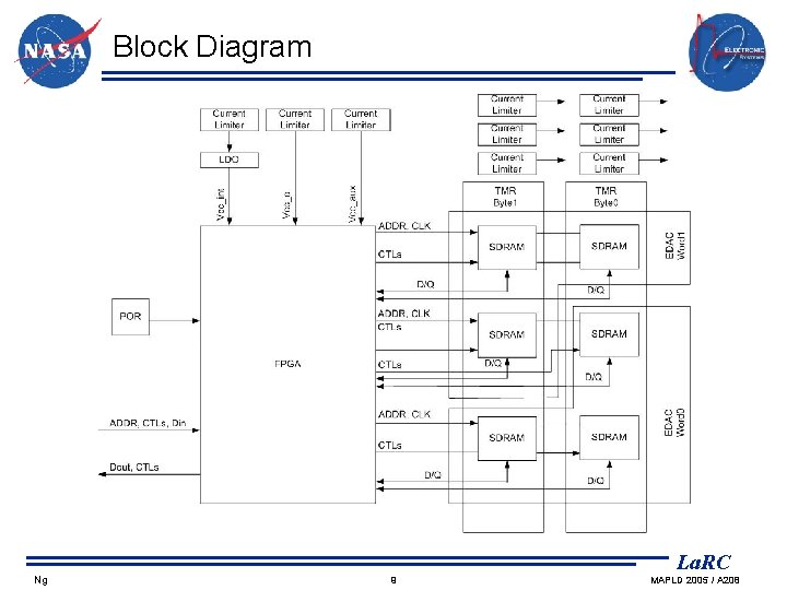
What is it ? • Radiation tolerant – Use commercial-off-the-shelf (COTS) components • Reprogrammable FPGA • High performance • Lower cost – Pick parts with applicable mitigation techniques • Shielding, over-current protection, triple module redundancy, FPGA configuration scrubbing • Intelligent – Reprogrammable FPGA • SDRAM controller • Capacity to add custom logic • Memory – Large capacity • SDRAM • Stack – 3 D vs 2 D, board space saving Ng La. RC 3 MAPLD 2005 / A 208

Goals • Large memory capacity – 256 MB EDAC • Single +3. 3 V power supply • Simple interface, LVTTL compatible • Throughput – 32 MWord write – 16 MWord read • Reprogram via the JTAG interface • Spare FPGA gate capacity for user application • Radiation characteristics – Total ionizing dose of 100 krad (Si) at 25 o C – SEU: best practice – SEL of 60 Me. V-cm 2/mg requirement • Operating temperature: -40 o C / +85 o C Ng La. RC 4 MAPLD 2005 / A 208

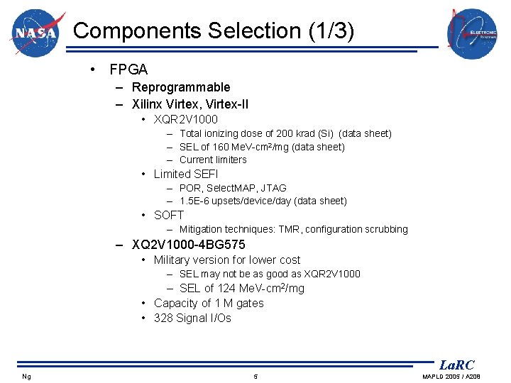
Components Selection (1/3) • FPGA – Reprogrammable – Xilinx Virtex, Virtex-II • XQR 2 V 1000 – Total ionizing dose of 200 krad (Si) (data sheet) – SEL of 160 Me. V-cm 2/mg (data sheet) – Current limiters • Limited SEFI – POR, Select. MAP, JTAG – 1. 5 E-6 upsets/device/day (data sheet) • SOFT – Mitigation techniques: TMR, configuration scrubbing – XQ 2 V 1000 -4 BG 575 • Military version for lower cost – SEL may not be as good as XQR 2 V 1000 – SEL of 124 Me. V-cm 2/mg • Capacity of 1 M gates • 328 Signal I/Os Ng La. RC 5 MAPLD 2005 / A 208

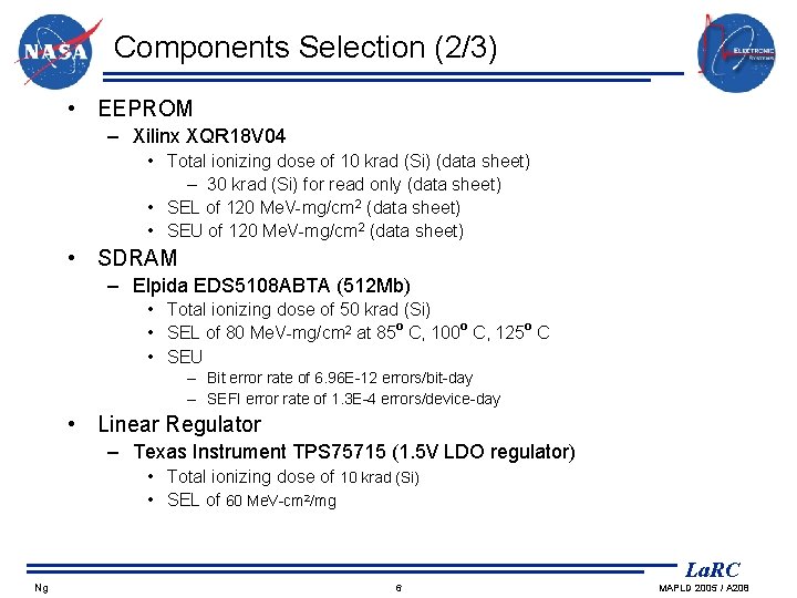
Components Selection (2/3) • EEPROM – Xilinx XQR 18 V 04 • Total ionizing dose of 10 krad (Si) (data sheet) – 30 krad (Si) for read only (data sheet) • SEL of 120 Me. V-mg/cm 2 (data sheet) • SEU of 120 Me. V-mg/cm 2 (data sheet) • SDRAM – Elpida EDS 5108 ABTA (512 Mb) • Total ionizing dose of 50 krad (Si) • SEL of 80 Me. V-mg/cm 2 at 85 o C, 100 o C, 125 o C • SEU – Bit error rate of 6. 96 E-12 errors/bit-day – SEFI error rate of 1. 3 E-4 errors/device-day • Linear Regulator – Texas Instrument TPS 75715 (1. 5 V LDO regulator) • Total ionizing dose of 10 krad (Si) • SEL of 60 Me. V-cm 2/mg Ng La. RC 6 MAPLD 2005 / A 208

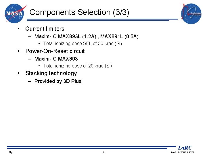
Components Selection (3/3) • Current limiters – Maxim-IC MAX 893 L (1. 2 A) , MAX 891 L (0. 5 A) • Total ionizing dose SEL of 30 krad (Si) • Power-On-Reset circuit – Maxim-IC MAX 803 • Total ionizing dose of 20 krad (Si) • Stacking technology – Provided by 3 D Plus Ng La. RC 7 MAPLD 2005 / A 208

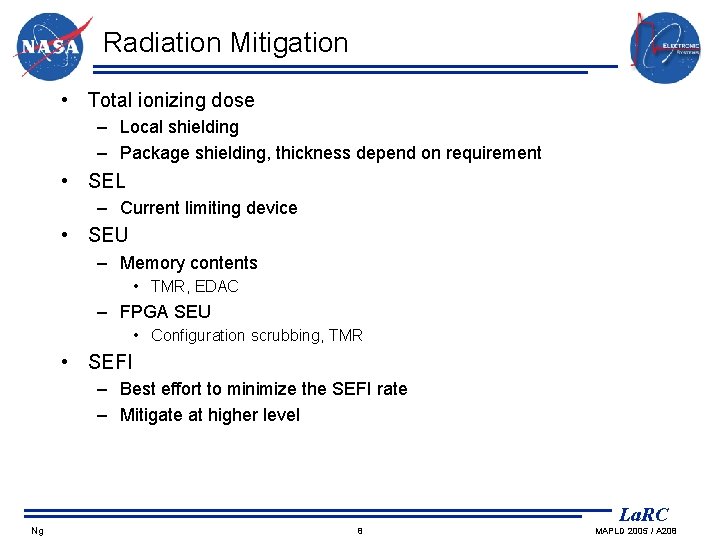
Radiation Mitigation • Total ionizing dose – Local shielding – Package shielding, thickness depend on requirement • SEL – Current limiting device • SEU – Memory contents • TMR, EDAC – FPGA SEU • Configuration scrubbing, TMR • SEFI – Best effort to minimize the SEFI rate – Mitigate at higher level Ng La. RC 8 MAPLD 2005 / A 208

Block Diagram Ng La. RC 9 MAPLD 2005 / A 208

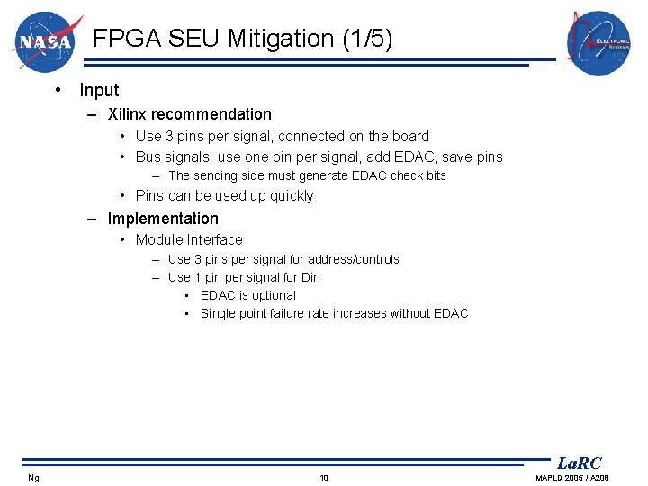
FPGA SEU Mitigation (1/5) • Input – Xilinx recommendation • Use 3 pins per signal, connected on the board • Bus signals: use one pin per signal, add EDAC, save pins – The sending side must generate EDAC check bits • Pins can be used up quickly – Implementation • Module Interface – Use 3 pins per signal for address/controls – Use 1 pin per signal for Din • EDAC is optional • Single point failure rate increases without EDAC Ng La. RC 10 MAPLD 2005 / A 208

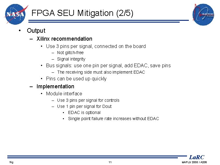
FPGA SEU Mitigation (2/5) • Output – Xilinx recommendation • Use 3 pins per signal, connected on the board – Not glitch-free – Signal integrity • Bus signals: use one pin per signal, add EDAC, save pins – The receiving side must also implement EDAC • Pins can be used up quickly – Implementation • Module interface – Use 3 pins per signal for controls – Use 1 pin per signal for Dout • EDAC is optional • Single point failure rate increases without EDAC Ng La. RC 11 MAPLD 2005 / A 208

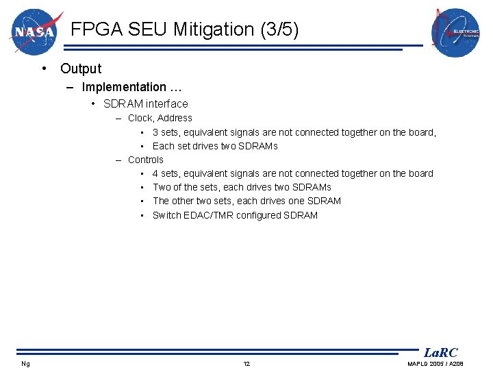
FPGA SEU Mitigation (3/5) • Output – Implementation … • SDRAM interface – Clock, Address • 3 sets, equivalent signals are not connected together on the board, • Each set drives two SDRAMs – Controls • 4 sets, equivalent signals are not connected together on the board • Two of the sets, each drives two SDRAMs • The other two sets, each drives one SDRAM • Switch EDAC/TMR configured SDRAM Ng La. RC 12 MAPLD 2005 / A 208

FPGA SEU Mitigation (4/5) • Bi-directional – Xilinx recommendation • Use 1 pin per signal • Path from voter to the pin becomes possible single point failure – Implementation • SDRAM Interface – TMR configured SDRAMs • 3 sets of data bus – EDAC configure SDRAMs • Use 1 pin per signal Ng La. RC 13 MAPLD 2005 / A 208

FPGA SEU Mitigation (5/5) • Implication on data integrity of the SDRAM contents – EDAC configured SDRAMs • 256 MB • Output drivers and input receivers are possible single point failure – TMR configured SDRAMs • 128 MB • No single point failure • Back ground SDRAMs content scrubbing Ng La. RC 14 MAPLD 2005 / A 208

XTMR Tool (1/4) • Fairly fast • Gates utilized – Average utilization cost of TMR is ~3. 2 x – RTIMS actual • 4. 3 x • Gates multiplier = 3 + 3 * (fraction of flops + fraction of I/Os) – It is closer to 3 x for design that is mostly gates – It is closer to 6 x for design that is mostly flops – RTIMS actual: 36% flops • Additional multiplier for design with SRL 16 Ng La. RC 15 MAPLD 2005 / A 208

XTMR Tool (2/4) • Internal performance degradation – Average performance impact of TMR is ~10% – RTIMS actual • ~20% • 6 logic levels original – Add a voter, 7 levels – ~15% performance impact • Longer routing – 3. 8 x gates – ~5% performance impact Ng La. RC 16 MAPLD 2005 / A 208

XTMR Tool (3/4) • I/O performance degradation • Input Pin – TMR • Voters after the FF • Lock the FF in the IOB – No TMR on input pin • • Ng 3 FFs after the input receiver Can’t lock the FF in the IOB Performance penalty RTIMS actual: increased from 1. 8 ns to 3. 6 ns La. RC 17 MAPLD 2005 / A 208

XTMR Tool (4/4) • Output Pin – Triplicate pin, tied together on board • • • Add Voter before the output driver Glitch Can’t lock the FF in the IOB Performance penalty Signal integrity – Not triplicating pin • • Add voter before the output driver Glitch Can’t lock the FF in the IOB Performance penalty – RTIMS actual: increased from 4. 5 ns to 6. 4 ns Ng La. RC 18 MAPLD 2005 / A 208

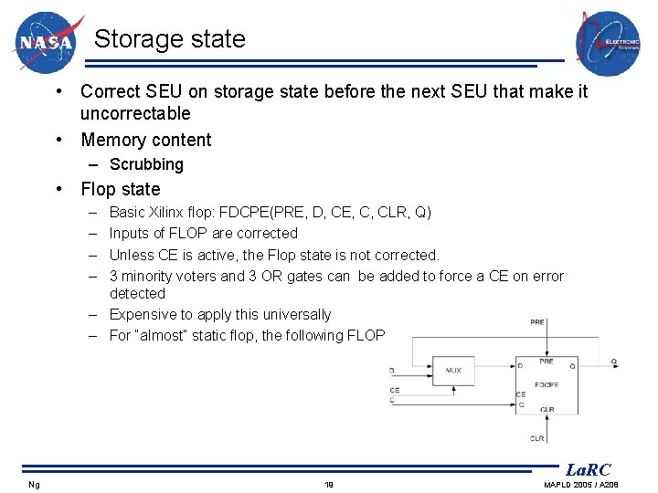
Storage state • Correct SEU on storage state before the next SEU that make it uncorrectable • Memory content – Scrubbing • Flop state – – Basic Xilinx flop: FDCPE(PRE, D, CE, C, CLR, Q) Inputs of FLOP are corrected Unless CE is active, the Flop state is not corrected. 3 minority voters and 3 OR gates can be added to force a CE on error detected – Expensive to apply this universally – For “almost” static flop, the following FLOP is used Ng La. RC 19 MAPLD 2005 / A 208

A few other things (1/4) • Digital Clock Manger – Use 3 DCMs for each DCM that is in the original design – DCM is a unit • SEU on a FLOP in the DCM – Corrected by configuration scrubbing – Reset only – 3 counters, each counter is clocked by a DCM – When one of the counter value is different from the other two, we know which DCM is operating differently than the others – Each counter is TMR so that a SEU on the counter other than the clock path will not produce an error Ng La. RC 20 MAPLD 2005 / A 208

A few other things (2/4) • Configuration scrubbing – Similar to Virtex – Virtex II • Whole configuration is loaded with 1 type 2 command • The order of configuration loading is – GCLK, CLB and IOB, Memory Content, and Memory Control – Script to split the loading into three type 2 command • GCLK, CLB, IOB • Memory control • Memory content – On power up the whole configuration is loaded – On scrubbing, only GCLK, CLB, IOB, and memory control are loaded Ng La. RC 21 MAPLD 2005 / A 208

A few other things (3/4) • Configuration scrubbing – Scrubber logic is TMR and it is part of the FPGA code – Master Select. Map for configuration with configuration clock continue to run after initial load – Scrubber logic is clocked by the configuration clock • The generation of the configuration clock becomes a possible single point failure • Can switch to Slave Select. Map and add an external oscillator Ng La. RC 22 MAPLD 2005 / A 208

A few other things (4/4) • Select. Map Interface SEFI detection – Implement a 16 x 1 distribute memory as SRL 16 with initial value of all zeros – Instruct XTMR not to convert it to registers – Write a signature into this memory prior to configuration scrubbing – This memory shall be clear because of the reloading of the CLB during configuration scrubbing – Read the memory content after configuration scrubbing – A non-zero content indicates scrubbing failure Ng La. RC 23 MAPLD 2005 / A 208

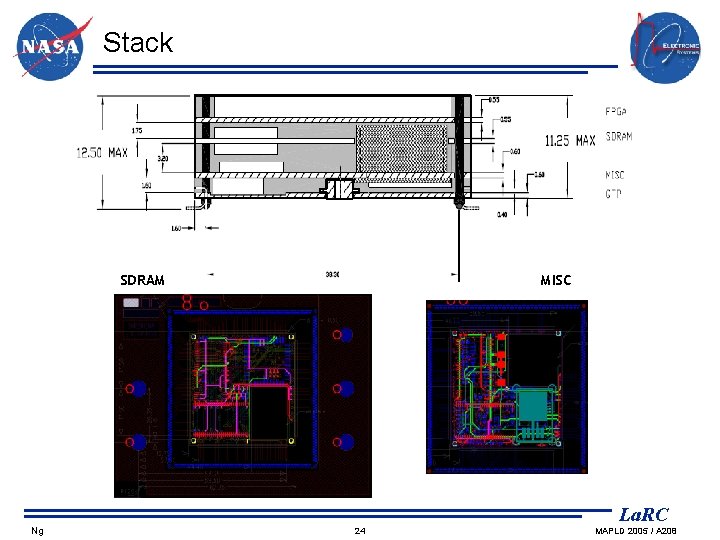
Stack SDRAM Ng MISC La. RC 24 MAPLD 2005 / A 208

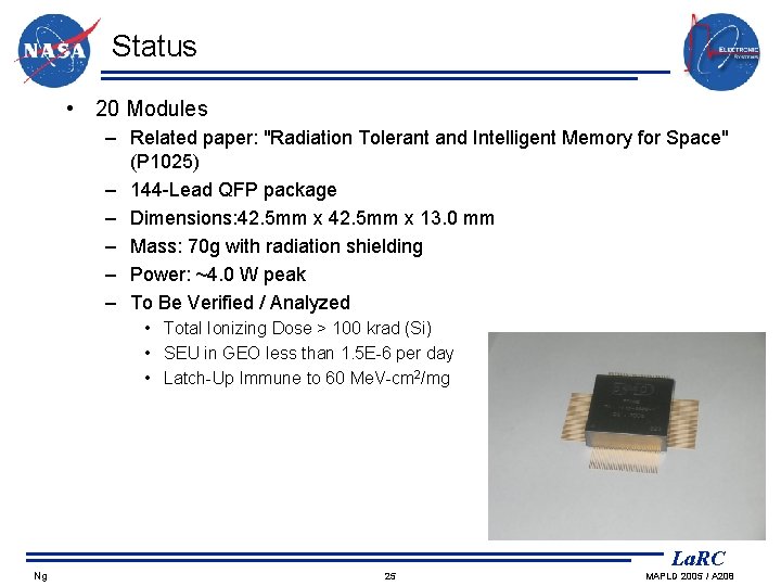
Status • 20 Modules – Related paper: "Radiation Tolerant and Intelligent Memory for Space" (P 1025) – 144 -Lead QFP package – Dimensions: 42. 5 mm x 13. 0 mm – Mass: 70 g with radiation shielding – Power: ~4. 0 W peak – To Be Verified / Analyzed • Total Ionizing Dose > 100 krad (Si) • SEU in GEO less than 1. 5 E-6 per day • Latch-Up Immune to 60 Me. V-cm 2/mg Ng La. RC 25 MAPLD 2005 / A 208

Future Work • VHDL and Place & Route – Works in progress • Minimize SEFI • Error detection and recording • Error recovery • What is the SEFI rate of RTIMS ? • Environment testing – – – Ng Life test (accelerated component life testing) 100 krad (Si) TID radiation tests SEL and SEU radiation tests Vacuum and temperature tests Mechanical stress tests Electrostatic discharge tests La. RC 26 MAPLD 2005 / A 208

Points to ponder • XTMR – Not a turn key process • • • Scrub memory content Almost static flop DCM failure detection and reset Glitch-free output is no longer glitch-free Signal integrity with dotted output – IO • 3 pins for one signal, EDAC • Tie the triplicate IO together vs carry three signals on the board with the voter implemented on the receiving side – One size does not fit all Ng La. RC 27 MAPLD 2005 / A 208