Radiation Tolerance of Silicon Detectors The Challenge for
- Slides: 10

Radiation Tolerance of Silicon Detectors The Challenge for Applications in Future High Energy Physics Experiments Gunnar Lindstroem, University of Hamburg Oslo University 17 -Jan-06 1

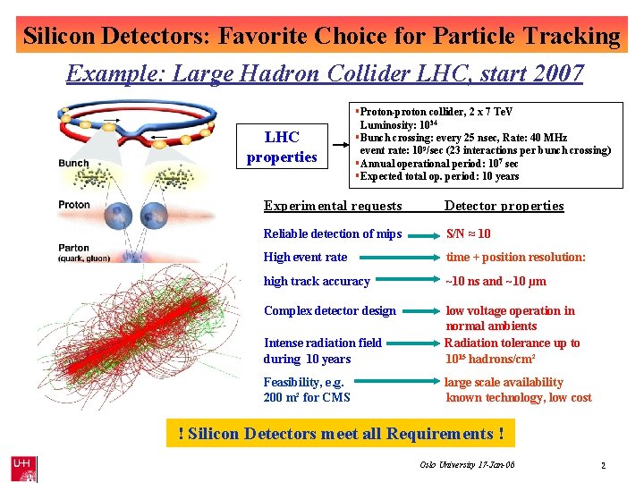
Silicon Detectors: Favorite Choice for Particle Tracking Example: Large Hadron Collider LHC, start 2007 LHC properties §Proton-proton collider, 2 x 7 Te. V Luminosity: 1034 §Bunch crossing: every 25 nsec, Rate: 40 MHz event rate: 109/sec (23 interactions per bunch crossing) §Annual operational period: 107 sec §Expected total op. period: 10 years Experimental requests Detector properties Reliable detection of mips S/N ≈ 10 High event rate time + position resolution: high track accuracy ~10 ns and ~10 µm Complex detector design low voltage operation in normal ambients Intense radiation field Radiation tolerance up to during 10 years 1015 hadrons/cm² Feasibility, e. g. 200 m² for CMS large scale availability known technology, low cost ! Silicon Detectors meet all Requirements ! Oslo University 17 -Jan-06 2

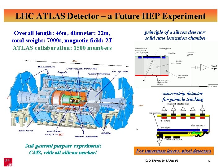
LHC ATLAS Detector – a Future HEP Experiment Overall length: 46 m, diameter: 22 m, total weight: 7000 t, magnetic field: 2 T ATLAS collaboration: 1500 members principle of a silicon detector: solid state ionization chamber micro-strip detector for particle tracking 2 nd general purpose experiment: CMS, with all silicon tracker! For innermost layers: pixel detectors Oslo University 17 -Jan-06 3

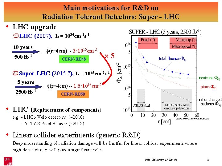
• Main motivations for R&D on Radiation Tolerant Detectors: Super - LHC upgrade LHC (2007), L = 1034 cm-2 s-1 10 years f(r=4 cm) ~ 3· 1015 cm-2 500 fb-1 CERN-RD 48 5 Super-LHC (2015 ? ), L = 1035 cm-2 s-1 5 years f(r=4 cm) ~ 1. 6· 1016 cm-2 2500 fb-1 CERN-RD 50 • LHC (Replacement of components) e. g. - LHCb Velo detectors (~2010) - ATLAS Pixel B-layer (~2012) • Linear collider experiments (generic R&D) Deep understanding of radiation damage will be fruitful for linear collider experiments where high doses of e, g will play a significant role. Oslo University 17 -Jan-06 4

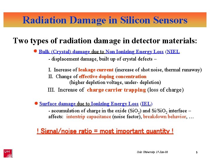
Radiation Damage in Silicon Sensors Two types of radiation damage in detector materials: Bulk (Crystal) damage due to Non Ionizing Energy Loss (NIEL - displacement damage, built up of crystal defects – I. Increase of leakage current (increase of shot noise, thermal runaway) II. Change of effective doping concentration (higher depletion voltage, under- depletion) III. Increase of charge carrier trapping (loss of charge) Surface damage due to Ionizing Energy Loss (IEL) - accumulation of charge in the oxide (Si. O 2) and Si/Si. O 2 interface – affects: interstrip capacitance (noise factor), breakdown behavior, … ! Signal/noise ratio = most important quantity ! Oslo University 17 -Jan-06 5

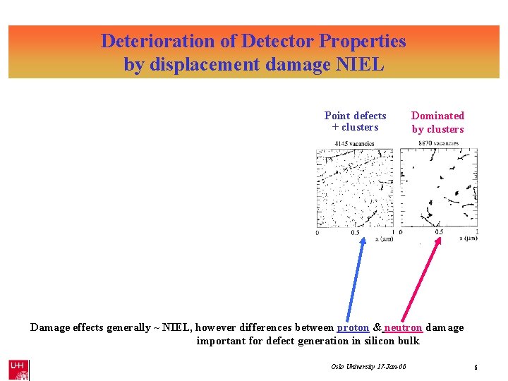
Deterioration of Detector Properties by displacement damage NIEL Point defects + clusters Dominated by clusters Damage effects generally ~ NIEL, however differences between proton & neutron damage important for defect generation in silicon bulk Oslo University 17 -Jan-06 6

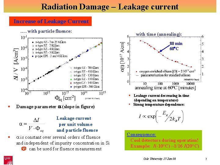
Radiation Damage – Leakage current Increase of Leakage Current …. with particle fluence: with time (annealing): 80 min 60 C § Leakage current decreasing in time § § Damage parameter (slope in figure) Leakage current per unit volume and particle fluence is constant over several orders of fluence and independent of impurity concentration in Si can be used for fluence measurement (depending on temperature) § Strong temperature dependence: Consequence: Cool detectors during operation! Example: I(-10°C) ~1/16 I(20°C) Oslo University 17 -Jan-06 7

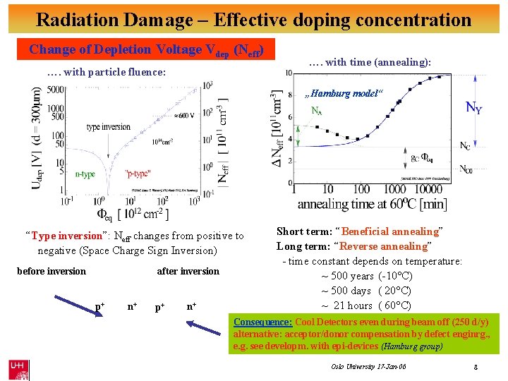
Radiation Damage – Effective doping concentration Change of Depletion Voltage Vdep (Neff) …. with particle fluence: …. with time (annealing): „Hamburg model“ “Type inversion”: Neff changes from positive to negative (Space Charge Sign Inversion) before inversion after inversion p+ n+ Short term: “Beneficial annealing” Long term: “Reverse annealing” - time constant depends on temperature: ~ 500 years (-10°C) ~ 500 days ( 20°C) ~ 21 hours ( 60°C) Consequence: Cool Detectors even during beam off (250 d/y) alternative: acceptor/donor compensation by defect enginrg. , e. g. see developm. with epi-devices (Hamburg group) Oslo University 17 -Jan-06 8

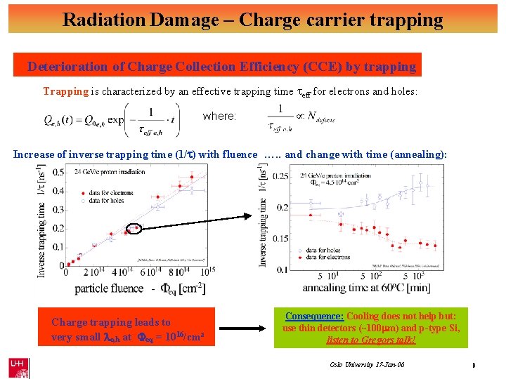
Radiation Damage – Charge carrier trapping Deterioration of Charge Collection Efficiency (CCE) by trapping Trapping is characterized by an effective trapping time eff for electrons and holes: where: Increase of inverse trapping time (1/ ) with fluence …. . and change with time (annealing): Charge trapping leads to very small le, h at Feq = 1016/cm² Consequence: Cooling does not help but: use thin detectors (~100 mm) and p-type Si, listen to Gregors talk! Oslo University 17 -Jan-06 9

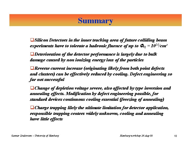
Summary q. Silicon Detectors in the inner tracking area of future colliding beam experiments have to tolerate a hadronic fluence of up to Feq = 1016/cm² q. Deterioration of the detector performance is largely due to bulk damage caused by non ionizing energy loss of the particles q. Reverse current increase (originating likely from both point defects and clusters) can be effectively reduced by cooling. Defect engineering so far not successful q. Change of depletion voltage severe, also affected by type inversion and annealing effects. Modification by defect engineering possible, for standard devices continuous cooling essential (freezing of annealing) q. Charge trapping lilely the ultimate limitation for detector application, responsible trapping centers widely unknown, cooling and annealing have little effects Gunnar Lindstroem – University of Hamburg workshop 24 -Aug-06 10