Radiation Tests of Candidate Memory Devices DDR 3
![SEE results – software conditioning Cross section [cm² / device] ▪ Elpida: reduces device SEE results – software conditioning Cross section [cm² / device] ▪ Elpida: reduces device](https://slidetodoc.com/presentation_image/4e6024cfe5e42a040c0769d0f1319a78/image-8.jpg)
![Total bit errors TID results – temperature dependence Temperature [°C] Total bit errors TID results – temperature dependence Temperature [°C]](https://slidetodoc.com/presentation_image/4e6024cfe5e42a040c0769d0f1319a78/image-14.jpg)
![TID results – idle current Samsung, 4 Gbit, room temperature Average current [m. A] TID results – idle current Samsung, 4 Gbit, room temperature Average current [m. A]](https://slidetodoc.com/presentation_image/4e6024cfe5e42a040c0769d0f1319a78/image-16.jpg)
- Slides: 31

Radiation Tests of Candidate Memory Devices DDR 3 SDRAM and NAND Flash Martin Herrmann, Kai Grürmann, Fritz Gliem, Hagen Schmidt ESTEC Technical Officer: Véronique Ferlet-Cavrois (TEC-QEC) Institut für Datentechnik, TU Braunschweig

Overview Part 1: DDR 3 SDRAM (M. Herrmann) ▫ Test bed ▫ SEE tests • • SEL Software conditioning Hard SEUs Hard SEU annealing ▫ TID tests • • • Band error pattern Error density Temperature dependence Annealing Idle current Part 2: NAND Flash (K. Grürmann) ESA/CNES Final Presentation days June 6, 2013 2

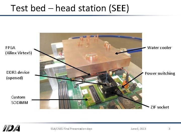
Test bed – head station (SEE) FPGA (Xilinx Virtex 6) Water cooler DDR 3 device (opened) Power switching Custom SODIMM ZIF socket ESA/CNES Final Presentation days June 6, 2013 3

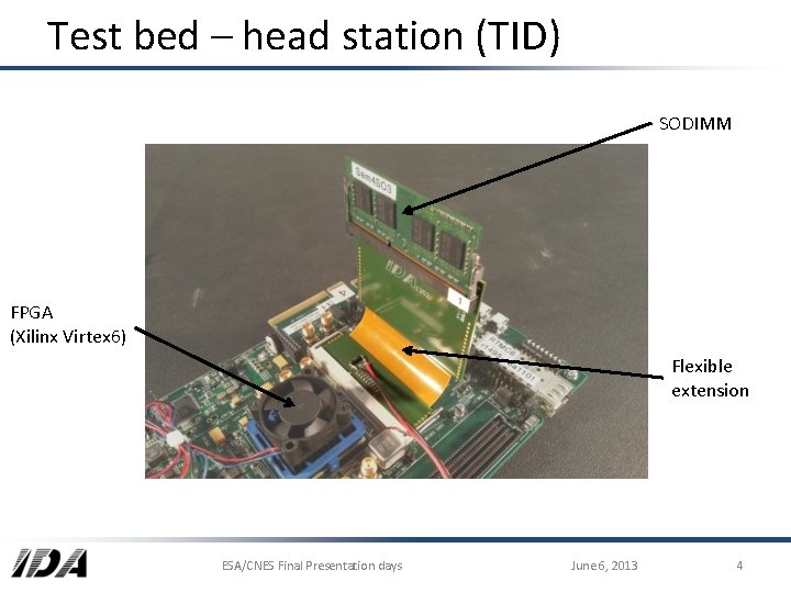
Test bed – head station (TID) SODIMM FPGA (Xilinx Virtex 6) Flexible extension ESA/CNES Final Presentation days June 6, 2013 4

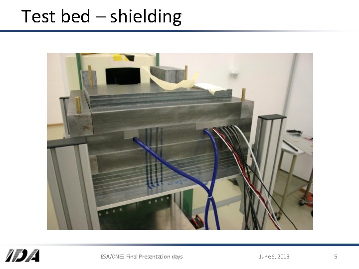
Test bed – shielding ESA/CNES Final Presentation days June 6, 2013 5

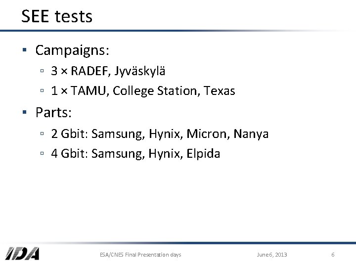
SEE tests ▪ Campaigns: ▫ 3 × RADEF, Jyväskylä ▫ 1 × TAMU, College Station, Texas ▪ Parts: ▫ 2 Gbit: Samsung, Hynix, Micron, Nanya ▫ 4 Gbit: Samsung, Hynix, Elpida ESA/CNES Final Presentation days June 6, 2013 6

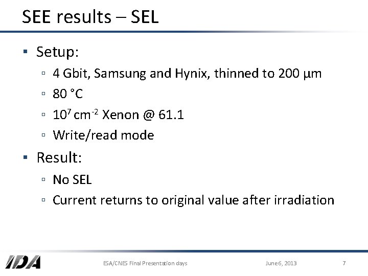
SEE results – SEL ▪ Setup: ▫ ▫ 4 Gbit, Samsung and Hynix, thinned to 200 µm 80 °C 107 cm-2 Xenon @ 61. 1 Write/read mode ▪ Result: ▫ No SEL ▫ Current returns to original value after irradiation ESA/CNES Final Presentation days June 6, 2013 7
![SEE results software conditioning Cross section cm² device Elpida reduces device SEE results – software conditioning Cross section [cm² / device] ▪ Elpida: reduces device](https://slidetodoc.com/presentation_image/4e6024cfe5e42a040c0769d0f1319a78/image-8.jpg)
SEE results – software conditioning Cross section [cm² / device] ▪ Elpida: reduces device SEFIs ▪ Samsung: no effect 1 E-4 1 E-5 1 E-6 1 E-7 4 Gbit Samsung without S/C 4 Gbit Samsung with S/C 4 Gbit Elpida without S/C 4 Gbit Elpida with S/C 1 E-8 1 E-9 1 E-10 0 10 20 30 40 50 LET [Me. V cm² / mg] ESA/CNES Final Presentation days 60 June 6, 2013 70 8

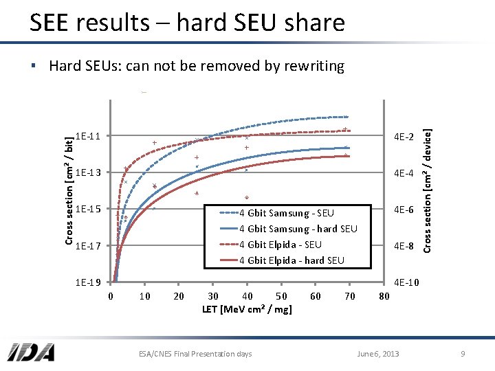
SEE results – hard SEU share 1 E-11 4 E-2 1 E-13 4 E-4 1 E-15 4 E-6 4 Gbit Samsung - SEU 4 Gbit Samsung - hard SEU 4 Gbit Elpida - hard SEU 1 E-17 4 E-8 1 E-19 Cross section [cm² / device] Cross section [cm² / bit] ▪ Hard SEUs: can not be removed by rewriting 4 E-10 0 10 20 30 40 50 LET [Me. V cm² / mg] ESA/CNES Final Presentation days 60 70 80 June 6, 2013 9

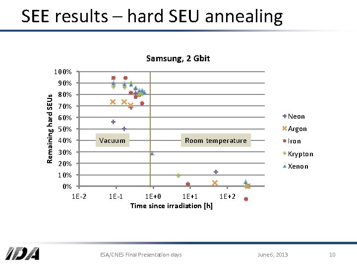
SEE results – hard SEU annealing Remaining hard SEUs Samsung, 2 Gbit 100% 90% 80% 70% 60% 50% 40% 30% 20% 10% 0% 1 E-2 Neon Argon Vacuum Room temperature Iron Krypton Xenon 1 E-1 1 E+0 1 E+1 1 E+2 Time since irradiation [h] ESA/CNES Final Presentation days June 6, 2013 10

TID campaigns ▪ Campaigns: ▫ 2 × ESTEC, Noordwijk ▪ Parts: ▫ In-Situ, 4 Gbit: Samsung ▫ Unbiased, 4 Gbit: Samsung, Hynix, Elpida ▫ Unbiased, 2 Gbit: Samsung, Hynix, Micron, Nanya ESA/CNES Final Presentation days June 6, 2013 11

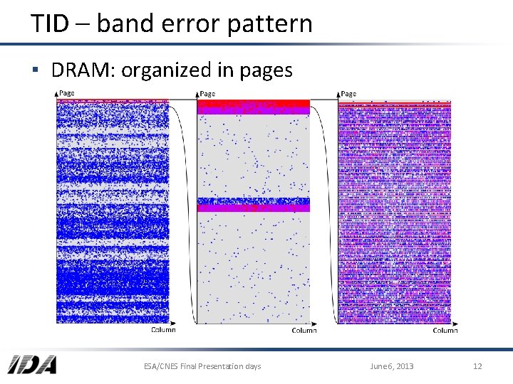
TID – band error pattern ▪ DRAM: organized in pages ESA/CNES Final Presentation days June 6, 2013 12

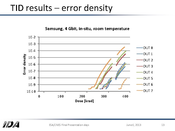
TID results – error density Samsung, 4 Gbit, in-situ, room temperature 1 E-2 1 E-3 DUT 0 Error density 1 E-4 DUT 1 1 E-5 DUT 2 1 E-6 DUT 3 1 E-7 DUT 4 1 E-8 DUT 5 1 E-9 DUT 6 1 E-10 DUT 7 0 100 200 Dose [krad] ESA/CNES Final Presentation days 300 400 June 6, 2013 13
![Total bit errors TID results temperature dependence Temperature C Total bit errors TID results – temperature dependence Temperature [°C]](https://slidetodoc.com/presentation_image/4e6024cfe5e42a040c0769d0f1319a78/image-14.jpg)
Total bit errors TID results – temperature dependence Temperature [°C]

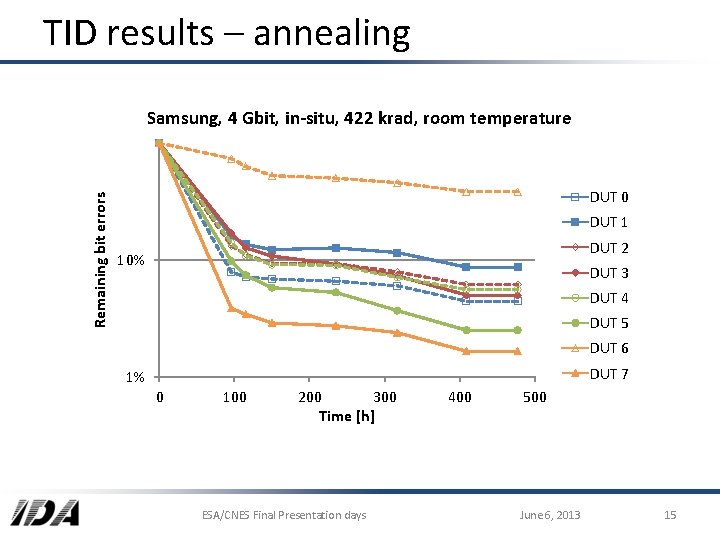
TID results – annealing Remaining bit errors Samsung, 4 Gbit, in-situ, 422 krad, room temperature DUT 0 DUT 1 DUT 2 10% DUT 3 DUT 4 DUT 5 DUT 6 DUT 7 1% 0 100 200 300 Time [h] ESA/CNES Final Presentation days 400 500 June 6, 2013 15
![TID results idle current Samsung 4 Gbit room temperature Average current m A TID results – idle current Samsung, 4 Gbit, room temperature Average current [m. A]](https://slidetodoc.com/presentation_image/4e6024cfe5e42a040c0769d0f1319a78/image-16.jpg)
TID results – idle current Samsung, 4 Gbit, room temperature Average current [m. A] 20 15 10 5 0 0 50 100 150 200 250 Dose [krad] ESA/CNES Final Presentation days 300 350 June 6, 2013 400 16

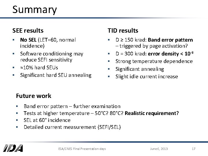
Summary SEE results TID results ▪ No SEL (LET=60, normal incidence) ▪ Software conditioning may reduce SEFI sensitivity ▪ ≈10% hard SEUs ▪ Significant hard SEU annealing ▪ D ≥ 150 krad: Band error pattern – triggered by page activation? ▪ D = 300 krad: error density < 10 -6 ▪ Strong temperature dependence ▪ Significant annealing ▪ Slight idle current increase Future work ▪ ▪ Band error pattern – further examination Tests at higher temperature – 50°C? 80°C? Realistic requirement? SEL at 60° incidence Detailed current measurement (SEFI/SEL) ESA/CNES Final Presentation days June 6, 2013 17

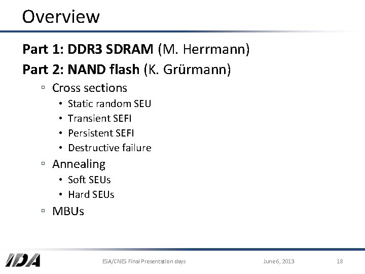
Overview Part 1: DDR 3 SDRAM (M. Herrmann) Part 2: NAND flash (K. Grürmann) ▫ Cross sections • • Static random SEU Transient SEFI Persistent SEFI Destructive failure ▫ Annealing • Soft SEUs • Hard SEUs ▫ MBUs ESA/CNES Final Presentation days June 6, 2013 18

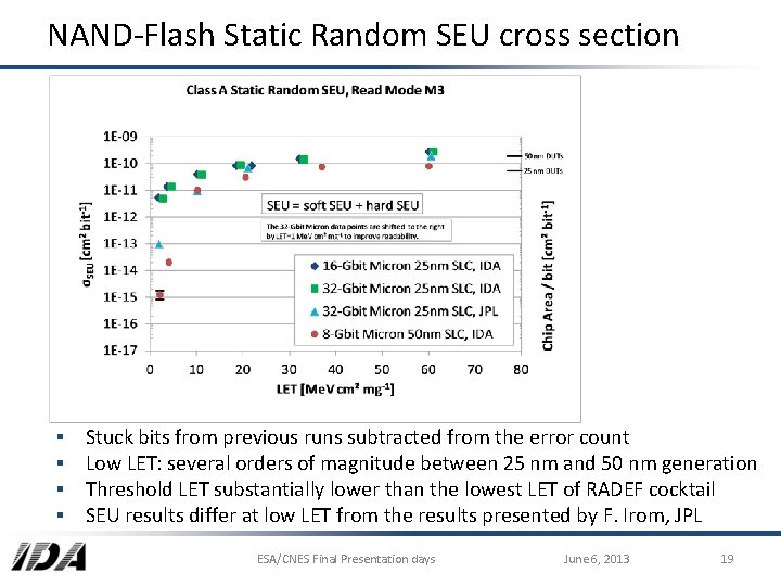
NAND-Flash Static Random SEU cross section ▪ ▪ Stuck bits from previous runs subtracted from the error count Low LET: several orders of magnitude between 25 nm and 50 nm generation Threshold LET substantially lower than the lowest LET of RADEF cocktail SEU results differ at low LET from the results presented by F. Irom, JPL ESA/CNES Final Presentation days June 6, 2013 19

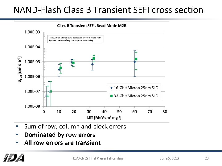
NAND-Flash Class B Transient SEFI cross section ▪ Sum of row, column and block errors ▪ Dominated by row errors ▪ All row errors are transient ESA/CNES Final Presentation days June 6, 2013 20

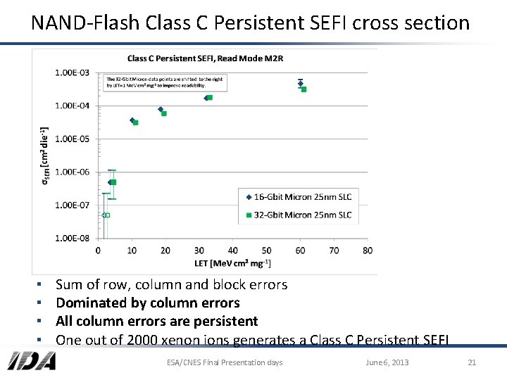
NAND-Flash Class C Persistent SEFI cross section ▪ ▪ Sum of row, column and block errors Dominated by column errors All column errors are persistent One out of 2000 xenon ions generates a Class C Persistent SEFI ESA/CNES Final Presentation days June 6, 2013 21

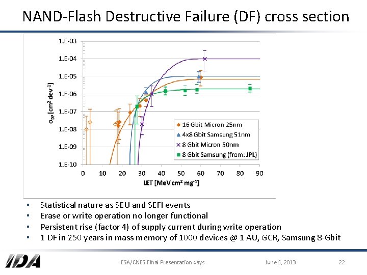
NAND-Flash Destructive Failure (DF) cross section ▪ ▪ Statistical nature as SEU and SEFI events Erase or write operation no longer functional Persistent rise (factor 4) of supply current during write operation 1 DF in 250 years in mass memory of 1000 devices @ 1 AU, GCR, Samsung 8 -Gbit ESA/CNES Final Presentation days June 6, 2013 22

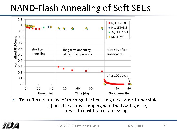
NAND-Flash Annealing of Soft SEUs ▪ Two effects: a) loss of the negative floating gate charge, irreversible b) positive charge trapping near the floating gate, reversible with time, annealing ESA/CNES Final Presentation days June 6, 2013 23

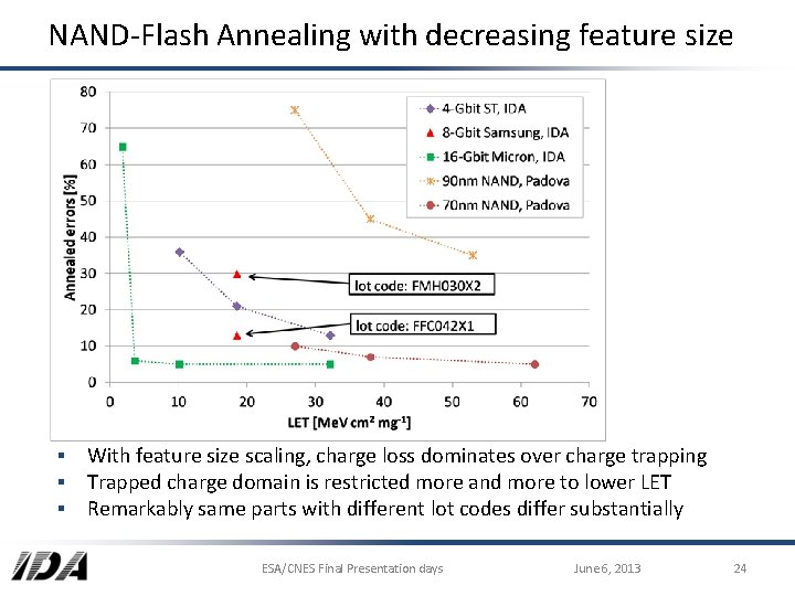
NAND-Flash Annealing with decreasing feature size ▪ With feature size scaling, charge loss dominates over charge trapping ▪ Trapped charge domain is restricted more and more to lower LET ▪ Remarkably same parts with different lot codes differ substantially ESA/CNES Final Presentation days June 6, 2013 24

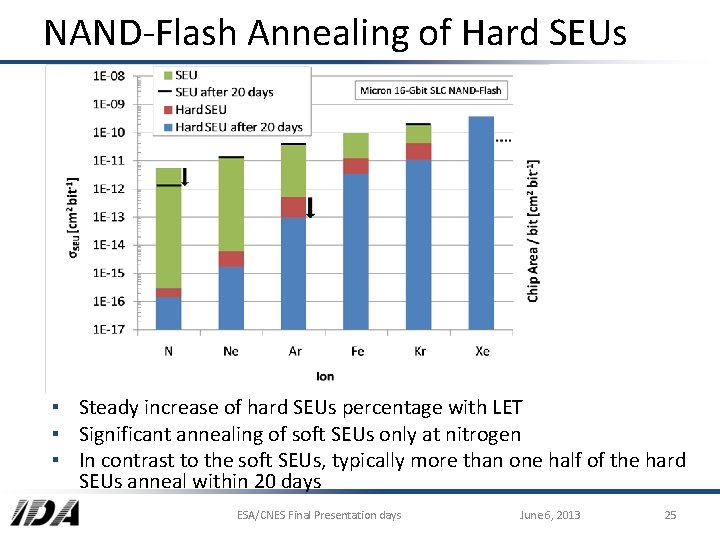
NAND-Flash Annealing of Hard SEUs ▪ Steady increase of hard SEUs percentage with LET ▪ Significant annealing of soft SEUs only at nitrogen ▪ In contrast to the soft SEUs, typically more than one half of the hard SEUs anneal within 20 days ESA/CNES Final Presentation days June 6, 2013 25

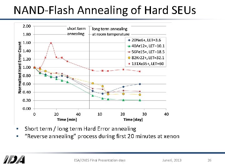
NAND-Flash Annealing of Hard SEUs ▪ Short term / long term Hard Error annealing ▪ “Reverse annealing” process during first 20 minutes at xenon ESA/CNES Final Presentation days June 6, 2013 26

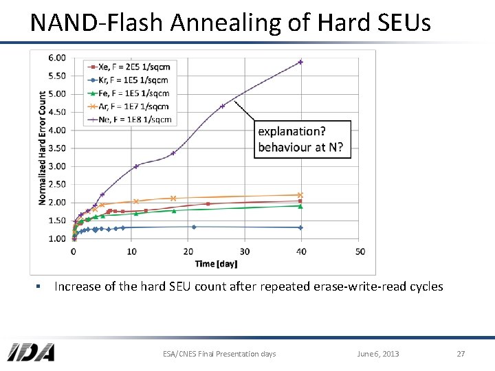
NAND-Flash Annealing of Hard SEUs ▪ Increase of the hard SEU count after repeated erase-write-read cycles ESA/CNES Final Presentation days June 6, 2013 27

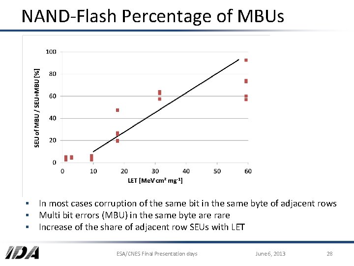
NAND-Flash Percentage of MBUs ▪ In most cases corruption of the same bit in the same byte of adjacent rows ▪ Multi bit errors (MBU) in the same byte are rare ▪ Increase of the share of adjacent row SEUs with LET ESA/CNES Final Presentation days June 6, 2013 28

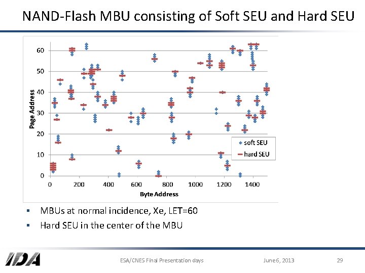
NAND-Flash MBU consisting of Soft SEU and Hard SEU ▪ MBUs at normal incidence, Xe, LET=60 ▪ Hard SEU in the center of the MBU ESA/CNES Final Presentation days June 6, 2013 29

Summary Addressed NAND-Flash topics ▪ SEU ▪ SEFI ▪ Destructive failure ▪ Annealing of soft and hard SEU ▪ MBU at normal incidence ESA/CNES Final Presentation days June 6, 2013 30

References ▪ Recent publications ▫ ▫ ▫ M. Herrmann et al. , “Heavy ion SEE test of 2 Gbit DDR 3 SDRAM”, RADECS Data Workshop, DW-28, 2011 K. Grürmann et al. , “Heavy Ion sensitivity of 16/32 -Gbit NAND-Flash and 4 -Gbit DDR 3 SDRAM”, IEEE NSREC Data Workshop, W-9, 2012 M. Herrmann et al. , “New SEE Test Results for 4 Gbit DDR 3 SDRAM”, RADECS Data Workshop, DW-25 L, 2012 K. Grürmann et al. , “New SEE Test Results of 16/32 -Gbit SLC NAND-Flash”, RADECS Data Workshop, DW-23 L, 2012 S. Gerardin et al. , “Radiation Effects in Flash Memories”, accepted for IEEE TNS Special Issue, 2013 M. Herrmann at al. , In-Situ TID Test of 4 -Gbit DDR 3 SDRAM Devices, submitted to NSREC Data Workshop, 2013 ▪ DDR 3 SDRAM technical notes ▪ NAND Flash technical notes ▫ ▫ ▫ M. Herrmann et al. , “TID Test of 4 Gbit DDR 3 SDRAM Devices”, TN-IDA-RAD-13/4 M. Herrmann et al. , “Heavy Ion SEE Test of 4 Gbit DDR 3 SDRAM Devices”, TN-IDA-RAD-13/1 M. Herrmann et al. , “Unbiased TID Test of 2 -Gbit and 4 -Gbit DDR 3 SDRAM Devices”, TN-IDA-RAD-13/9 K. Grürmann et al. , “Heavy Ion SEE Test of 2 -Gbit DDR 3 SDRAM Devices and of 8 -Gbit NAND-Flash Memory Devices, RADEF Jyväskylä, May 23 – 27, 2011”, Test Report, TN-IDA-RAD-11/5 B K. Grürmann et al. , “Heavy Ion SEE Test of 16 -Gbit/32 -Gbit Micron SLC NAND-Flash Memory Devices, RADEF Jyväskylä, Jan. 9 – 13, 2012, RADEF Jyväskylä, April 16 – 20, 2012”, Test Report, TN-IDA-RAD-12/12 K. Grürmann et al. , “Heavy Ion SEE Test of 4 x 8 -Gbit Samsung and 16 -Gbit Micron SLC NAND-Flash Memory Devices, TAMU Texas, December 4 – 7, 2012”, Test Report, TN-IDA-RAD-13/2 B ESA/CNES Final Presentation days June 6, 2013 31