Radiation test results PSI facility Amplifiers INA 111
- Slides: 15

Radiation test results PSI facility Amplifiers: INA 111 BU, LM 7372, MAX 4238 Voltage reference: ADR 434 BRZ Preparation, development, test and analysis by Pascal Oser, Eleftherios Fadakis, Gilles Foucard, Julien Mekki, Paul Peronnard, Raffaello Secondo, Giovanni Spiezia Group: 02/10/2020 EN-STI-ECE 1

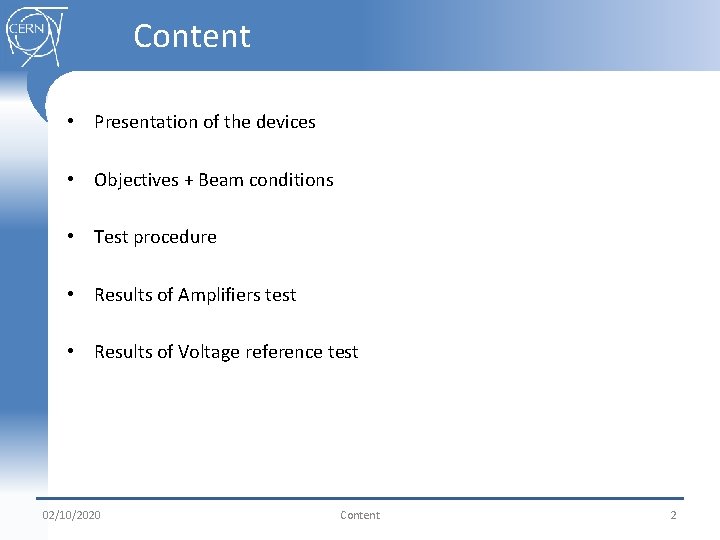
Content • Presentation of the devices • Objectives + Beam conditions • Test procedure • Results of Amplifiers test • Results of Voltage reference test 02/10/2020 Content 2

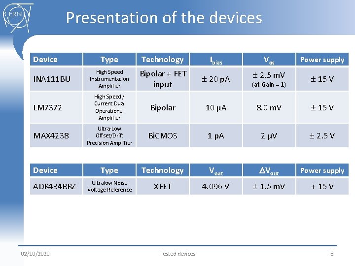
Presentation of the devices Device INA 111 BU LM 7372 MAX 4238 Device ADR 434 BRZ 02/10/2020 Type Technology Ibias Vos High Speed Instrumentation Amplifier Bipolar + FET input 20 p. A 2. 5 m. V 15 V High Speed / Current Dual Operational Amplifier Bipolar 10 µA 8. 0 m. V 15 V Ultra-Low Offset/Drift Precision Amplifier Bi. CMOS 1 p. A 2 µV 2. 5 V Type Technology Vout Power supply Ultralow Noise Voltage Reference XFET 4. 096 V 1. 5 m. V 15 V Tested devices (at Gain = 1) Power supply 3

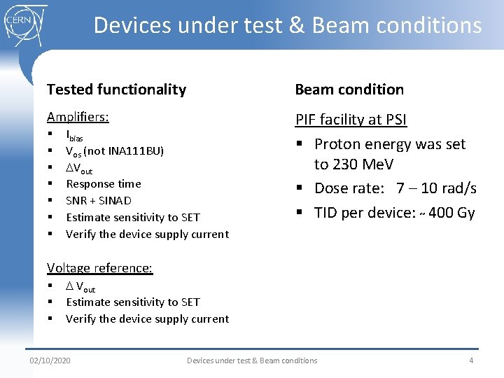
Devices under test & Beam conditions Tested functionality Beam condition Amplifiers: PIF facility at PSI § Proton energy was set to 230 Me. V § Dose rate: 7 – 10 rad/s § TID per device: ~ 400 Gy § § § § Ibias Vos (not INA 111 BU) Vout Response time SNR + SINAD Estimate sensitivity to SET Verify the device supply current Voltage reference: § § § Vout Estimate sensitivity to SET Verify the device supply current 02/10/2020 Devices under test & Beam conditions 4

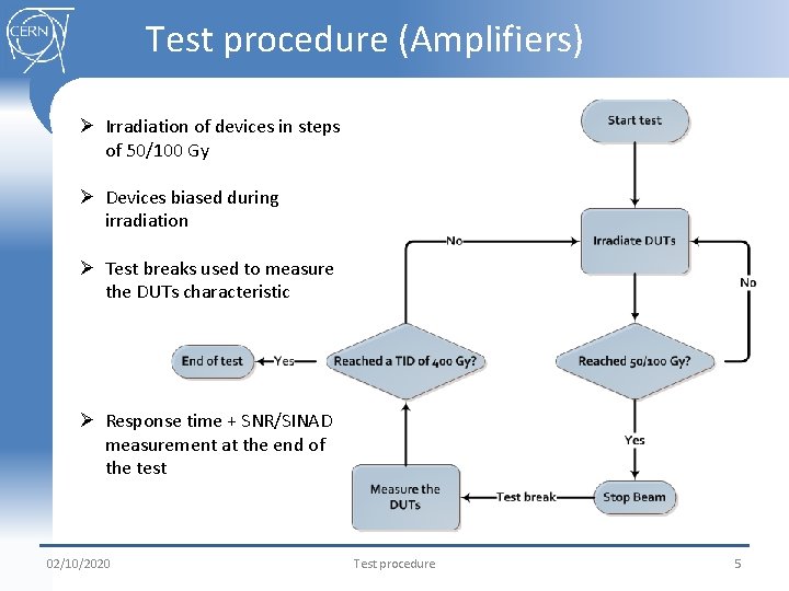
Test procedure (Amplifiers) Ø Irradiation of devices in steps of 50/100 Gy Ø Devices biased during irradiation Ø Test breaks used to measure the DUTs characteristic Ø Response time + SNR/SINAD measurement at the end of the test 02/10/2020 Test procedure 5

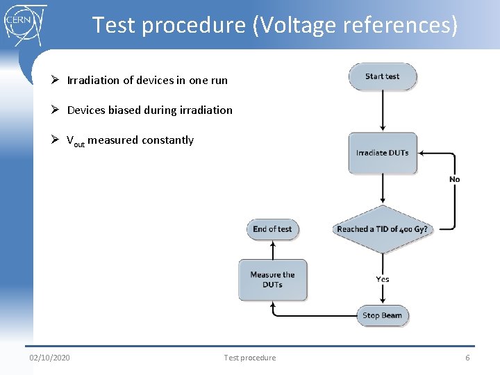
Test procedure (Voltage references) Ø Irradiation of devices in one run Ø Devices biased during irradiation Ø Vout measured constantly 02/10/2020 Test procedure 6

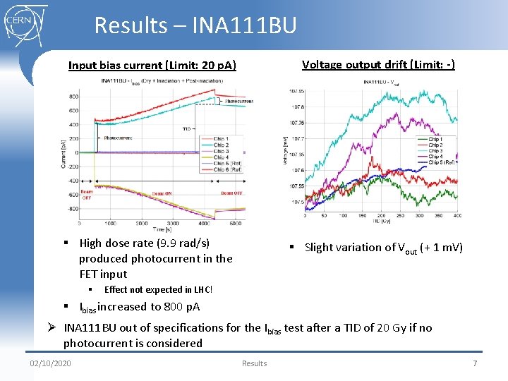
Results – INA 111 BU Voltage output drift (Limit: -) Input bias current (Limit: 20 p. A) § High dose rate (9. 9 rad/s) produced photocurrent in the FET input § § Slight variation of Vout (+ 1 m. V) Effect not expected in LHC! § Ibias increased to 800 p. A Ø INA 111 BU out of specifications for the Ibias test after a TID of 20 Gy if no photocurrent is considered 02/10/2020 Results 7

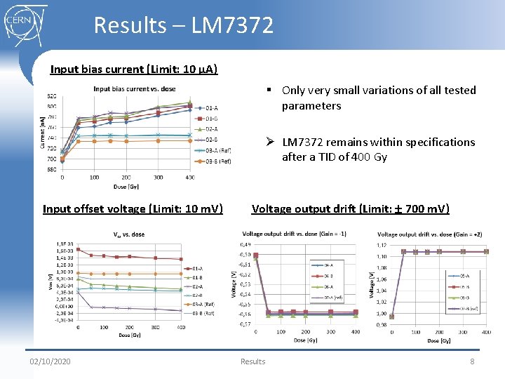
Results – LM 7372 Input bias current (Limit: 10 µA) § Only very small variations of all tested parameters Ø LM 7372 remains within specifications after a TID of 400 Gy Input offset voltage (Limit: 10 m. V) 02/10/2020 Voltage output drift (Limit: 700 m. V) Results 8

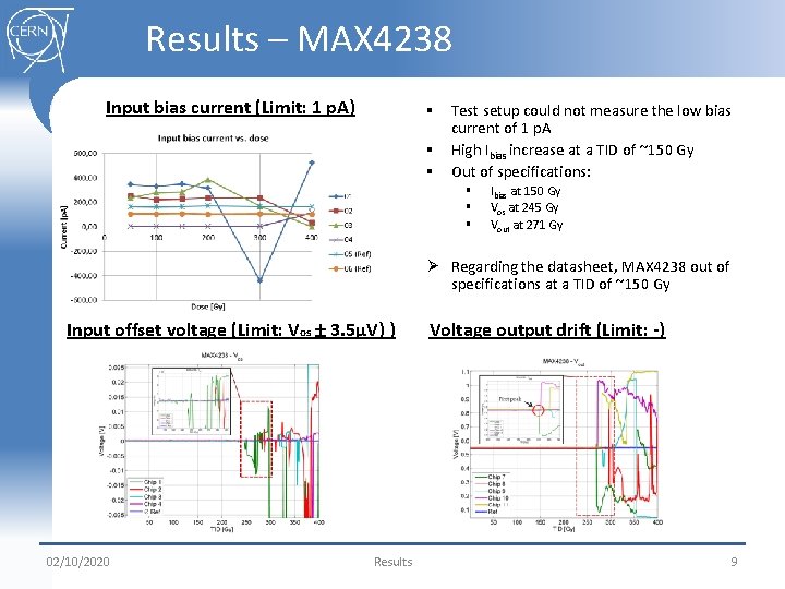
Results – MAX 4238 Input bias current (Limit: 1 p. A) § Test setup could not measure the low bias current of 1 p. A § High Ibias increase at a TID of ~150 Gy § Out of specifications: § § § Ibias at 150 Gy Vos at 245 Gy Vout at 271 Gy Ø Regarding the datasheet, MAX 4238 out of specifications at a TID of ~150 Gy Input offset voltage (Limit: Vos 3. 5µV) ) 02/10/2020 Results Voltage output drift (Limit: -) 9

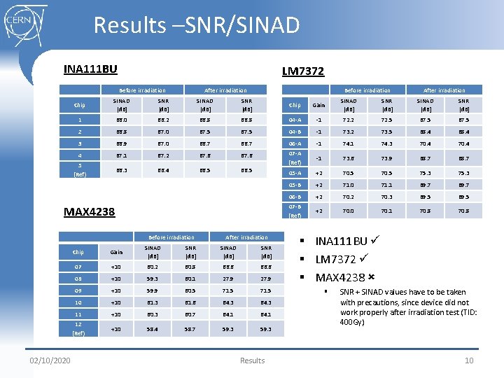
Results –SNR/SINAD INA 111 BU LM 7372 Before irradiation After irradiation Chip SINAD [d. B] SNR [d. B] Chip Gain SINAD [d. B] SNR [d. B] 1 66. 0 66. 2 66. 8 04 -A -1 72. 2 72. 5 67. 5 2 66. 8 67. 0 67. 5 04 -B -1 73. 2 73. 5 68. 4 3 66. 9 67. 0 66. 7 06 -A -1 74. 3 70. 4 4 67. 1 67. 2 67. 6 5 (Ref) -1 73. 6 73. 9 68. 7 66. 3 66. 4 66. 5 07 -A (Ref) 05 -A +2 70. 5 75. 3 05 -B +2 71. 0 71. 1 69. 7 06 -B +2 70. 3 69. 5 07 -B (Ref) +2 70. 0 70. 1 70. 8 MAX 4238 02/10/2020 Before irradiation After irradiation Chip Gain SINAD [d. B] SNR [d. B] 07 +10 60. 2 60. 8 66. 6 08 +10 59. 3 60. 1 27. 9 09 +10 59. 9 60. 5 71. 5 10 +10 61. 3 61. 6 64. 3 11 +10 60. 3 60. 7 64. 1 12 (Ref) +10 58. 4 58. 7 59. 3 Results § INA 111 BU § LM 7372 § MAX 4238 § SNR + SINAD values have to be taken with precautions, since device did not work properly after irradiation test (TID: 400 Gy) 10

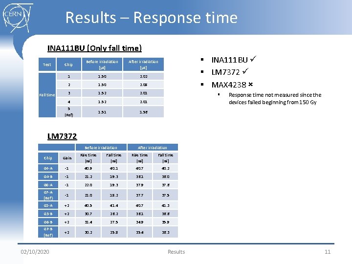
Results – Response time INA 111 BU (Only fall time) Test Fall time Chip Before irradiation [µs] After irradiation [µs] 1 1. 50 2. 02 2 1. 50 2. 08 3 1. 52 2. 01 4 1. 52 2. 01 5 (Ref) 1. 51 1. 56 § INA 111 BU § LM 7372 § MAX 4238 § Response time not measured since the devices failed beginning from 150 Gy LM 7372 Before irradiation After irradiation Chip Gain Rise time [ns] 04 -A -1 40. 9 40. 1 40. 7 40. 2 04 -B -1 21. 2 19. 3 36. 1 36. 0 06 -A -1 22. 0 19. 3 37. 9 37. 6 07 -A (Ref) -1 21. 0 18. 2 37. 7 37. 5 05 -A +2 40. 5 41. 4 40. 7 41. 3 05 -B +2 30. 7 26. 2 36. 1 36. 6 06 -B +2 31. 4 27. 5 34. 9 35. 9 07 -B (Ref) +2 30. 2 25. 8 35. 4 36. 3 02/10/2020 Fall time [ns] Rise time [ns] Fall time [ns] Results 11

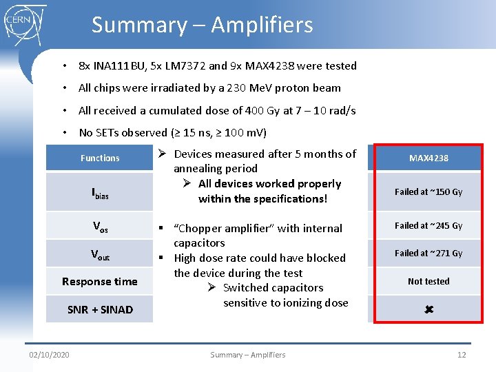
Summary – Amplifiers • 8 x INA 111 BU, 5 x LM 7372 and 9 x MAX 4238 were tested • All chips were irradiated by a 230 Me. V proton beam • All received a cumulated dose of 400 Gy at 7 – 10 rad/s • No SETs observed (≥ 15 ns, ≥ 100 m. V) Functions Ibias Vout Response time SNR + SINAD 02/10/2020 Ø Devices measured after 5 LM 7372 months of INA 111 BU annealing period Failed at ~20 Gy Ø All devices worked properly (Photocurrent not within the specifications! considered) amplifier” with internal § “Chopper capacitors rate could have blocked § High dose the device during the test Ø Switched capacitors sensitive to ionizing dose Summary – Amplifiers MAX 4238 Failed at ~150 Gy Failed at ~245 Gy Failed at ~271 Gy Not tested 12

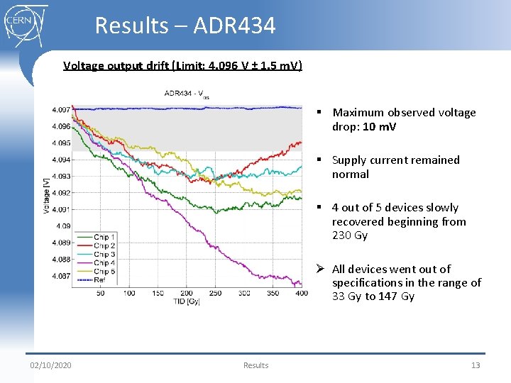
Results – ADR 434 Voltage output drift (Limit: 4. 096 V ± 1. 5 m. V) § Maximum observed voltage drop: 10 m. V § Supply current remained normal § 4 out of 5 devices slowly recovered beginning from 230 Gy Ø All devices went out of specifications in the range of 33 Gy to 147 Gy 02/10/2020 Results 13

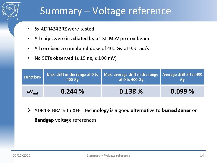
Summary – Voltage reference • 5 x ADR 434 BRZ were tested • All chips were irradiated by a 230 Me. V proton beam • All received a cumulated dose of 400 Gy at 9. 9 rad/s • No SETs observed (≥ 15 ns, ≥ 100 m. V) Functions Max. drift in the range of 0 to 400 Gy ΔVout 0. 244 % Max. average drift in the range Average drift after 400 of 0 to 400 Gy Gy 0. 138 % 0. 099 % Ø ADR 434 BRZ with XFET technology is a good alternative to buried Zener or Bandgap voltage references 02/10/2020 Summary – Voltage reference 14

Thank you for your attention! Any questions? Presentation according to Radiation Test Report EDMS: 1279855 (Amplifiers) EDMS: 1280154 (Voltage reference) 02/10/2020 15