Radiation damage in silicon detectors Radiation damage in



- Slides: 19


Radiation damage in silicon detectors

Radiation damage in silicon detectors

Radiation damage in silicon detectors

Radiation damage in silicon detectors:

Outline________________ • Introduction • Radiation damage • How do we study it • Effects • Conclusions 1

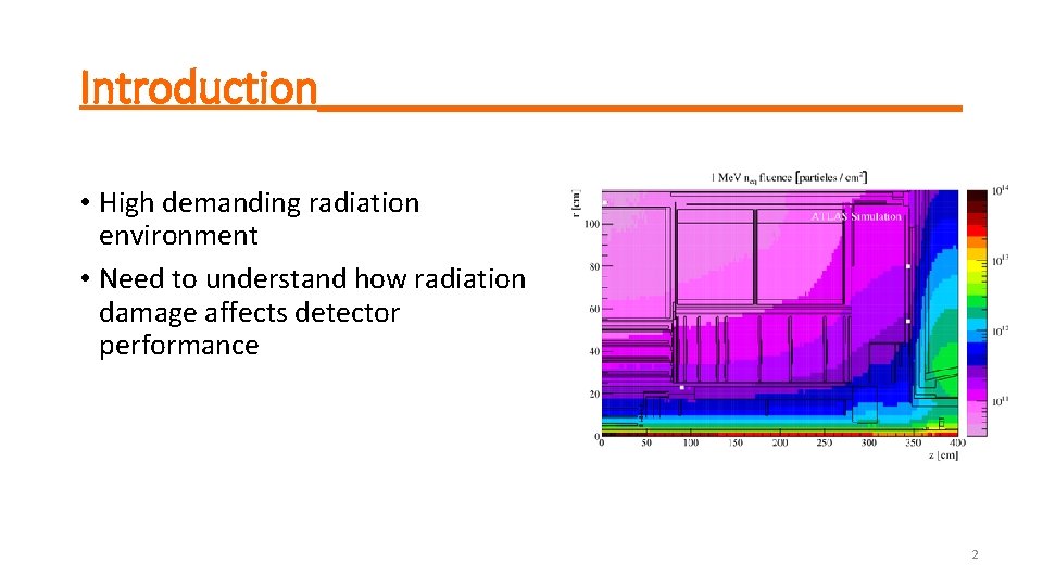
Introduction______________ • High demanding radiation environment • Need to understand how radiation damage affects detector performance 2

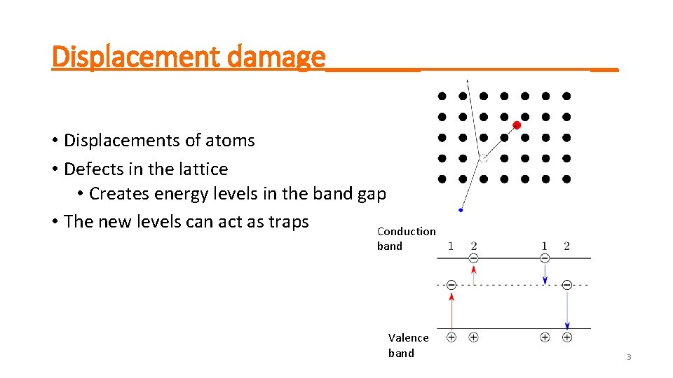
Displacement damage__________ • Displacements of atoms • Defects in the lattice • Creates energy levels in the band gap • The new levels can act as traps Conduction band Valence band 3

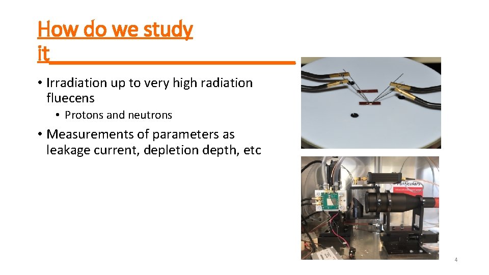
How do we study it___________ • Irradiation up to very high radiation fluecens • Protons and neutrons • Measurements of parameters as leakage current, depletion depth, etc 4

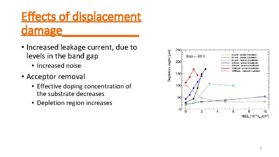
Effects of displacement damage______ • Increased leakage current, due to levels in the band gap • Increased noise • Acceptor removal • Effective doping concentration of the substrate decreases • Depletion region increases 5

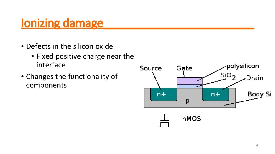
Ionizing damage____________ • Defects in the silicon oxide • Fixed positive charge near the interface • Changes the functionality of components 6

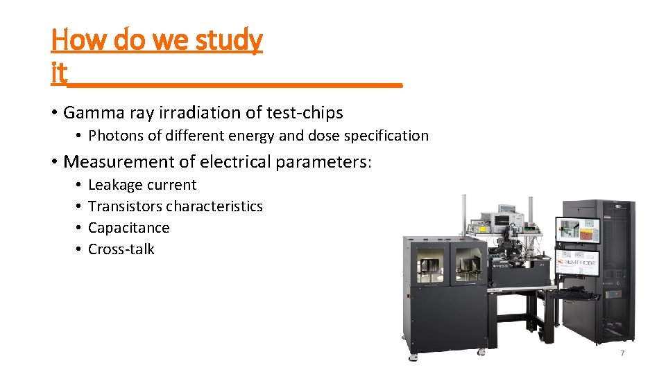
How do we study it___________ • Gamma ray irradiation of test-chips • Photons of different energy and dose specification • Measurement of electrical parameters: • • Leakage current Transistors characteristics Capacitance Cross-talk 7

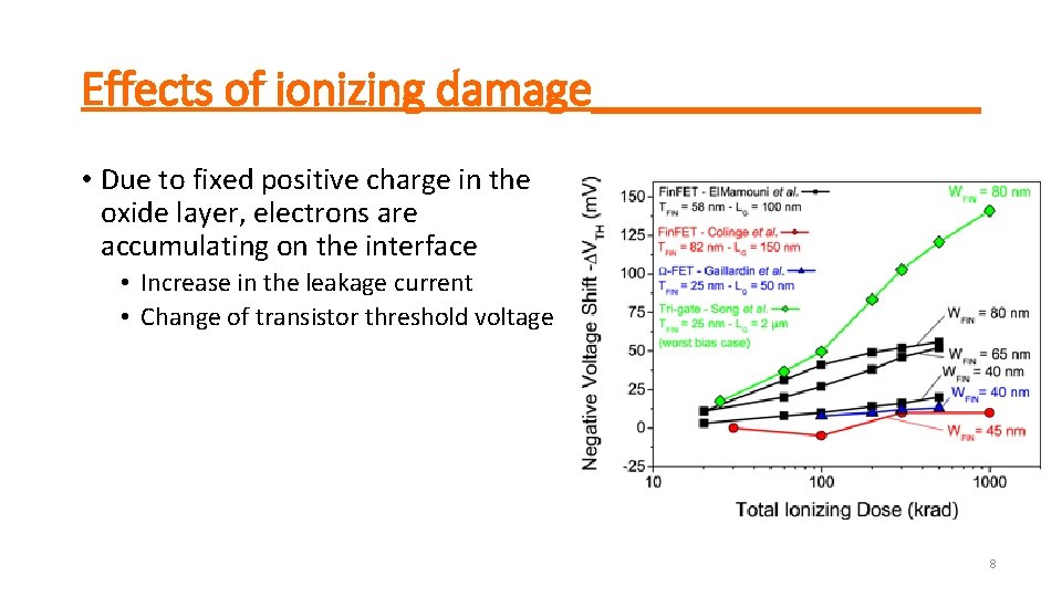
Effects of ionizing damage________ • Due to fixed positive charge in the oxide layer, electrons are accumulating on the interface • Increase in the leakage current • Change of transistor threshold voltage 8

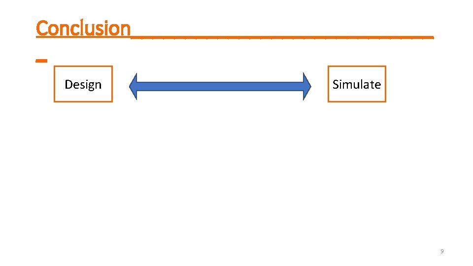
Conclusion______________ _ Design Simulate 9

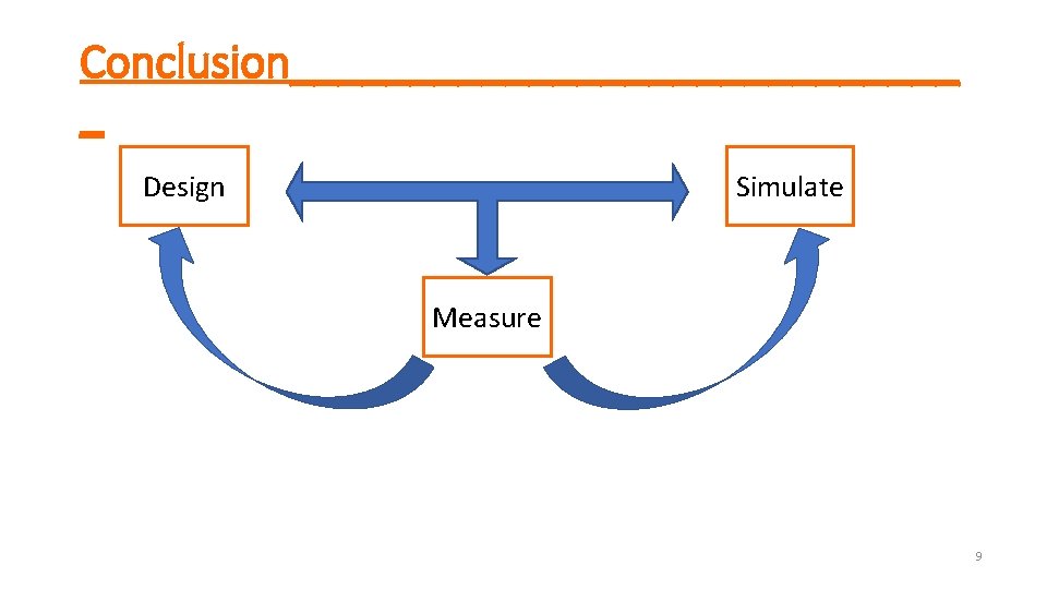
Conclusion______________ _ Design Simulate Measure 9

Conclusion______________ _ Design Simulate Measure 9

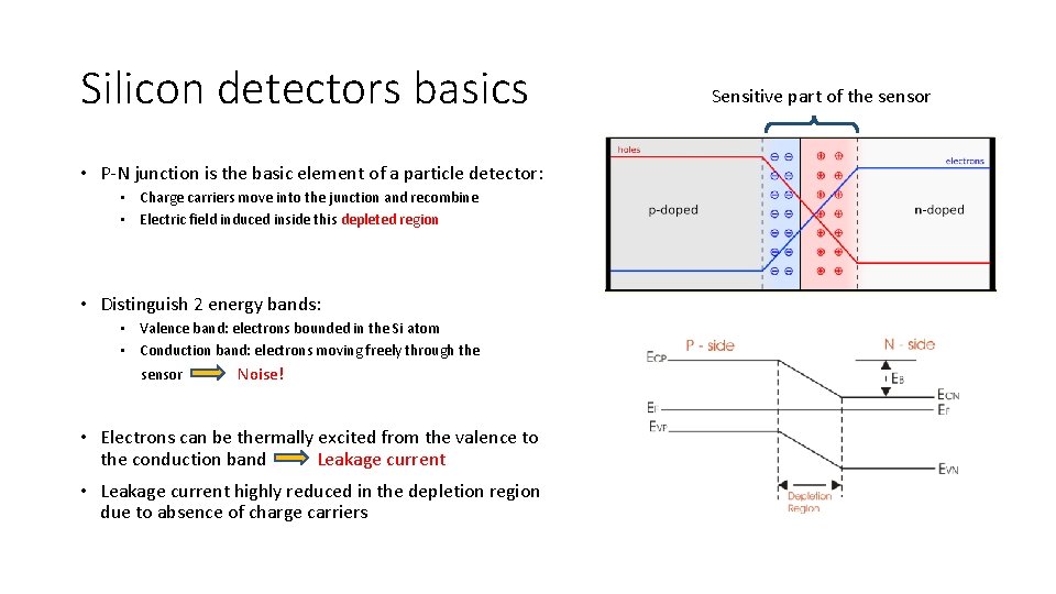
Silicon detectors basics • P-N junction is the basic element of a particle detector: • Charge carriers move into the junction and recombine • Electric field induced inside this depleted region • Distinguish 2 energy bands: • Valence band: electrons bounded in the Si atom • Conduction band: electrons moving freely through the sensor Noise! • Electrons can be thermally excited from the valence to the conduction band Leakage current • Leakage current highly reduced in the depletion region due to absence of charge carriers Sensitive part of the sensor