Radiation Damage in Sentaurus TCAD David Pennicard University

- Slides: 25

Radiation Damage in Sentaurus TCAD David Pennicard – University of Glasgow

Overview • Introduction to trap models • Radiation damage effects and defects • P-type damage model • Some example simulations • Sentaurus Device command file

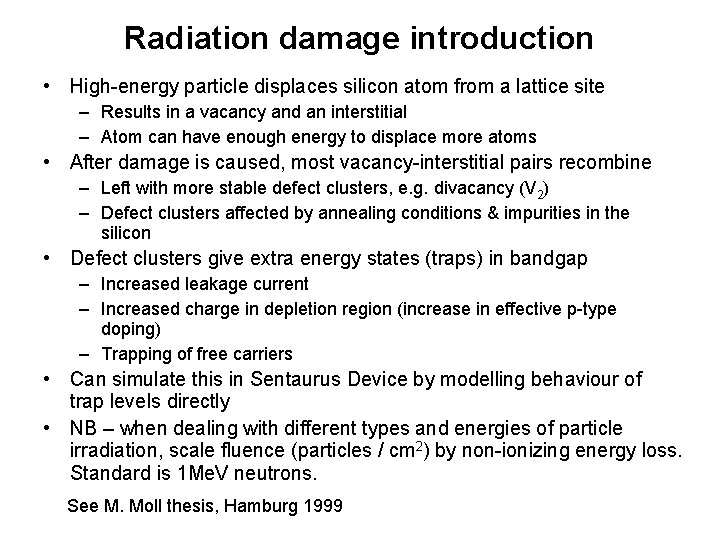
Radiation damage introduction • High-energy particle displaces silicon atom from a lattice site – Results in a vacancy and an interstitial – Atom can have enough energy to displace more atoms • After damage is caused, most vacancy-interstitial pairs recombine – Left with more stable defect clusters, e. g. divacancy (V 2) – Defect clusters affected by annealing conditions & impurities in the silicon • Defect clusters give extra energy states (traps) in bandgap – Increased leakage current – Increased charge in depletion region (increase in effective p-type doping) – Trapping of free carriers • Can simulate this in Sentaurus Device by modelling behaviour of trap levels directly • NB – when dealing with different types and energies of particle irradiation, scale fluence (particles / cm 2) by non-ionizing energy loss. Standard is 1 Me. V neutrons. See M. Moll thesis, Hamburg 1999

Traps in Sentaurus Device • A statement added to the Physics section can describe the traps: Physics (material="Silicon") { Traps ( (Acceptor Level from. Cond. Band Conc=1. 613 e 15 Energy. Mid=0. 42 e. Xsection=9. 5 E-15 h. Xsection=9. 5 E-14) ) } • Parameters – Acceptor: trap has –ve charge when occupied by electron, 0 charge when occupied by hole. (Donor has +ve charge when occupied by hole) – Level: specifies how we describe energy level. Here, we give the energy below the conduction band. Energy. Mid gives the energy difference – Concentration: given in cm-3 – Electron cross-section: proportional to probability of electron moving between trap and conduction band - σe – Hole cross-section: likewise, proportional to chance of carrier moving between valence band trap level - σp

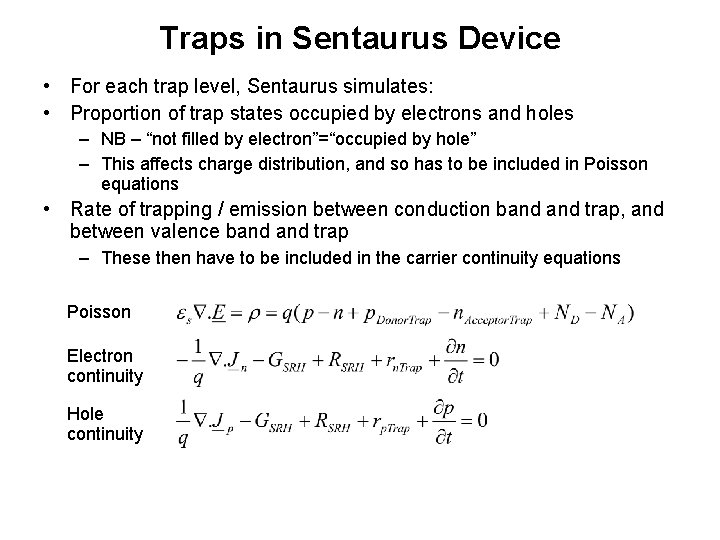
Traps in Sentaurus Device • For each trap level, Sentaurus simulates: • Proportion of trap states occupied by electrons and holes – NB – “not filled by electron”=“occupied by hole” – This affects charge distribution, and so has to be included in Poisson equations • Rate of trapping / emission between conduction band trap, and between valence band trap – These then have to be included in the carrier continuity equations Poisson Electron continuity Hole continuity

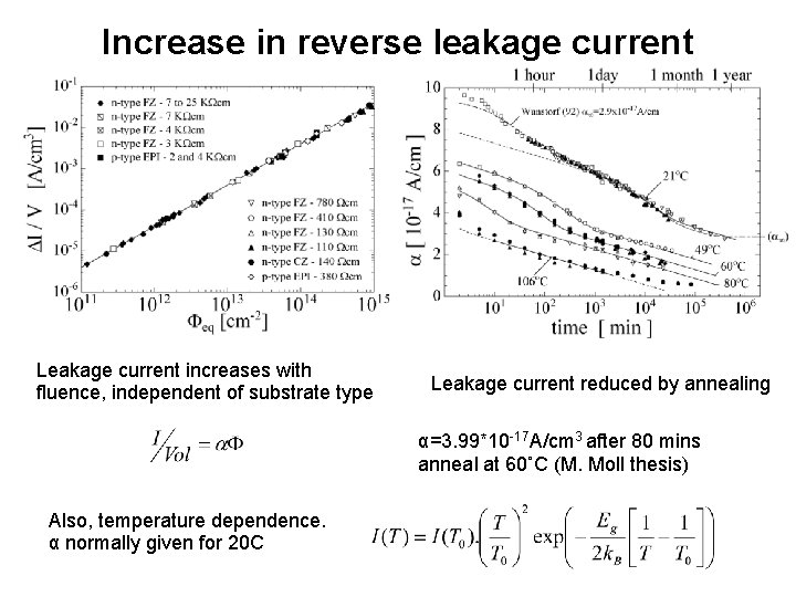
Increase in reverse leakage current Leakage current increases with fluence, independent of substrate type Leakage current reduced by annealing α=3. 99*10 -17 A/cm 3 after 80 mins anneal at 60˚C (M. Moll thesis) Also, temperature dependence. α normally given for 20 C

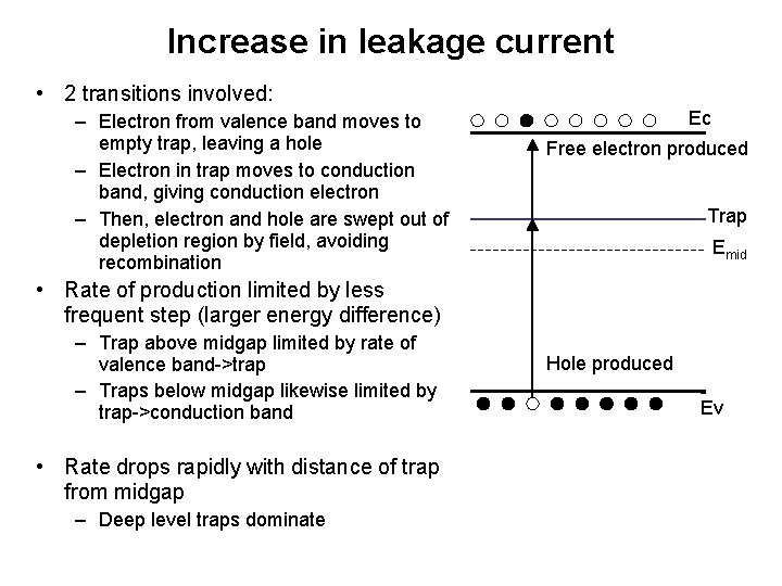
Increase in leakage current • 2 transitions involved: – Electron from valence band moves to empty trap, leaving a hole – Electron in trap moves to conduction band, giving conduction electron – Then, electron and hole are swept out of depletion region by field, avoiding recombination Ec Free electron produced Trap Emid • Rate of production limited by less frequent step (larger energy difference) – Trap above midgap limited by rate of valence band->trap – Traps below midgap likewise limited by trap->conduction band • Rate drops rapidly with distance of trap from midgap – Deep level traps dominate Hole produced Ev

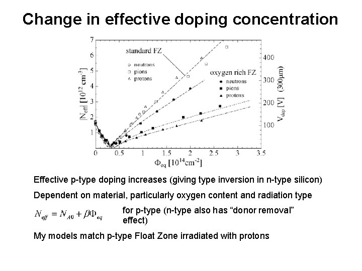
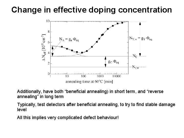
Change in effective doping concentration Effective p-type doping increases (giving type inversion in n-type silicon) Dependent on material, particularly oxygen content and radiation type for p-type (n-type also has “donor removal” effect) My models match p-type Float Zone irradiated with protons

Change in effective doping concentration Additionally, have both “beneficial annealing) in short term, and “reverse annealing” in long term Typically, test detectors after beneficial annealing, to try to find stable damage level All this implies very complicated defect behaviour!

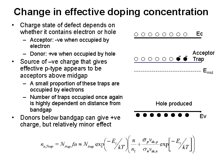
Change in effective doping concentration • Charge state of defect depends on whether it contains electron or hole – Acceptor: -ve when occupied by electron – Donor: +ve when occupied by hole • Source of –ve charge that gives effective p-type appears to be acceptors above midgap – A small proportion of these traps are occupied by electrons – Number of traps occupied once again is highly dependent on distance from bandgap • Donors below bandgap can give +ve charge, but relatively minor effect Ec - - Acceptor Trap Emid Hole produced Ev

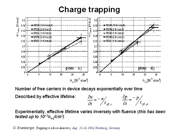
Charge trapping Number of free carriers in device decays exponentially over time Described by effective lifetime: Experimentally, effective lifetime varies inversely with fluence (this has been tested up to 1015 neq/cm 2) G. Kramberger, Trapping in silicon detectors, Aug. 23 -24, 2006, Hamburg, Germany

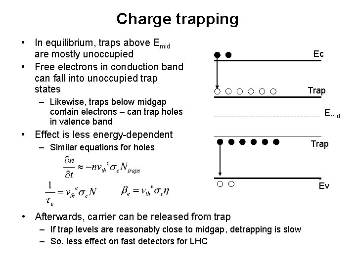
Charge trapping • In equilibrium, traps above Emid are mostly unoccupied • Free electrons in conduction band can fall into unoccupied trap states – Likewise, traps below midgap contain electrons – can trap holes in valence band • Effect is less energy-dependent – Similar equations for holes Ec Trap Emid Trap Ev • Afterwards, carrier can be released from trap – If trap levels are reasonably close to midgap, detrapping is slow – So, less effect on fast detectors for LHC

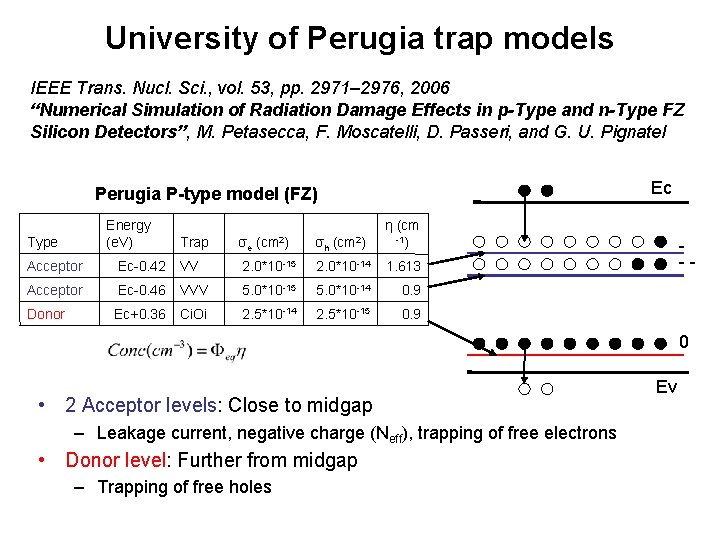
University of Perugia trap models IEEE Trans. Nucl. Sci. , vol. 53, pp. 2971– 2976, 2006 “Numerical Simulation of Radiation Damage Effects in p-Type and n-Type FZ Silicon Detectors”, M. Petasecca, F. Moscatelli, D. Passeri, and G. U. Pignatel Ec Perugia P-type model (FZ) Energy (e. V) Type Trap σe (cm 2) σh (cm 2) η (cm -1) Acceptor Ec-0. 42 VV 2. 0*10 -15 2. 0*10 -14 1. 613 Acceptor Ec-0. 46 VVV 5. 0*10 -15 5. 0*10 -14 0. 9 Donor Ec+0. 36 Ci. Oi 2. 5*10 -14 2. 5*10 -15 0. 9 -- 0 • 2 Acceptor levels: Close to midgap – Leakage current, negative charge (Neff), trapping of free electrons • Donor level: Further from midgap – Trapping of free holes Ev

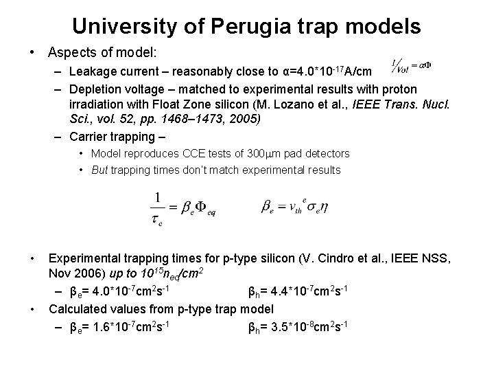
University of Perugia trap models • Aspects of model: – Leakage current – reasonably close to α=4. 0*10 -17 A/cm – Depletion voltage – matched to experimental results with proton irradiation with Float Zone silicon (M. Lozano et al. , IEEE Trans. Nucl. Sci. , vol. 52, pp. 1468– 1473, 2005) – Carrier trapping – • Model reproduces CCE tests of 300 m pad detectors • But trapping times don’t match experimental results • • Experimental trapping times for p-type silicon (V. Cindro et al. , IEEE NSS, Nov 2006) up to 1015 neq/cm 2 – βe= 4. 0*10 -7 cm 2 s-1 βh= 4. 4*10 -7 cm 2 s-1 Calculated values from p-type trap model – βe= 1. 6*10 -7 cm 2 s-1 βh= 3. 5*10 -8 cm 2 s-1

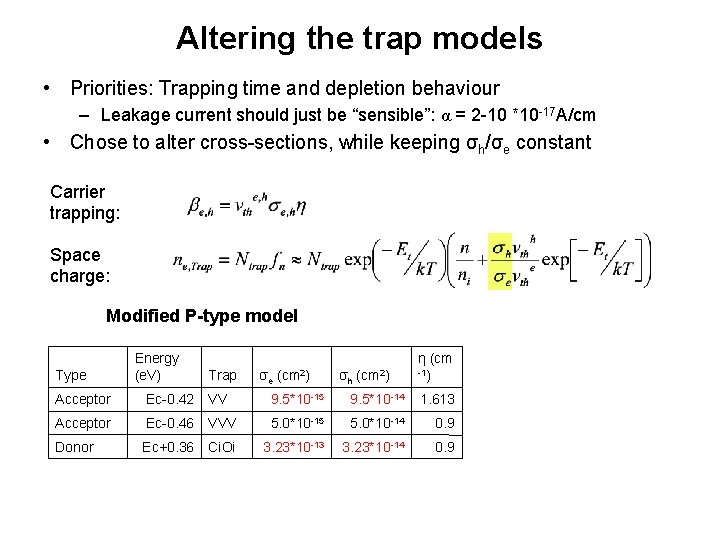
Altering the trap models • Priorities: Trapping time and depletion behaviour – Leakage current should just be “sensible”: α = 2 -10 *10 -17 A/cm • Chose to alter cross-sections, while keeping σh/σe constant Carrier trapping: Space charge: Modified P-type model Type Energy (e. V) Trap σe (cm 2) σh (cm 2) η (cm -1) Acceptor Ec-0. 42 VV 9. 5*10 -15 9. 5*10 -14 1. 613 Acceptor Ec-0. 46 VVV 5. 0*10 -15 5. 0*10 -14 0. 9 Donor Ec+0. 36 Ci. Oi 3. 23*10 -13 3. 23*10 -14 0. 9

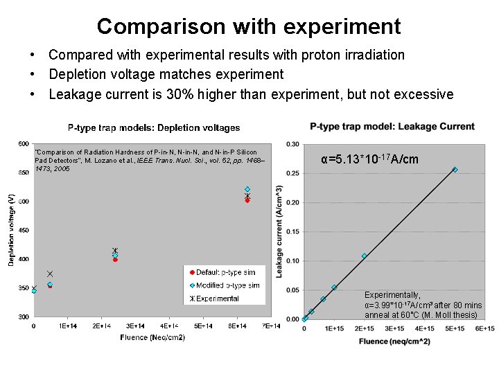
Comparison with experiment • Compared with experimental results with proton irradiation • Depletion voltage matches experiment • Leakage current is 30% higher than experiment, but not excessive “Comparison of Radiation Hardness of P-in-N, N-in-N, and N-in-P Silicon Pad Detectors”, M. Lozano et al. , IEEE Trans. Nucl. Sci. , vol. 52, pp. 1468– 1473, 2005 -17 A/cm α=5. 13*10 α=3. 75*10 -17 A/cm Experimentally, α=3. 99*10 -17 A/cm 3 after 80 mins anneal at 60˚C (M. Moll thesis)

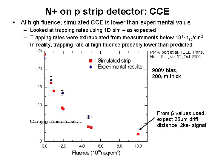
N+ on p strip detector: CCE • At high fluence, simulated CCE is lower than experimental value – Looked at trapping rates using 1 D sim – as expected – Trapping rates were extrapolated from measurements below 1015 neq/cm 2 – In reality, trapping rate at high fluence probably lower than predicted PP Allport et al. , IEEE Trans. Nucl. Sci. , vol 52, Oct 2005 900 V bias, 280 m thick From β values used, expect 25μm drift distance, 2 ke- signal

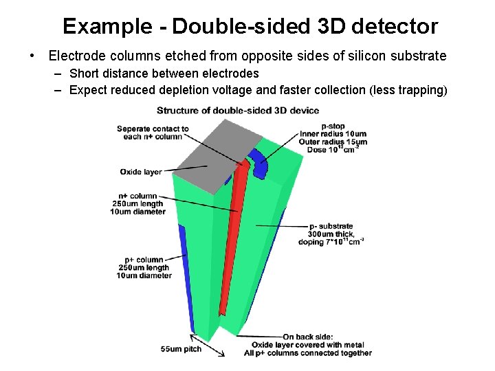
Example - Double-sided 3 D detector • Electrode columns etched from opposite sides of silicon substrate – Short distance between electrodes – Expect reduced depletion voltage and faster collection (less trapping)

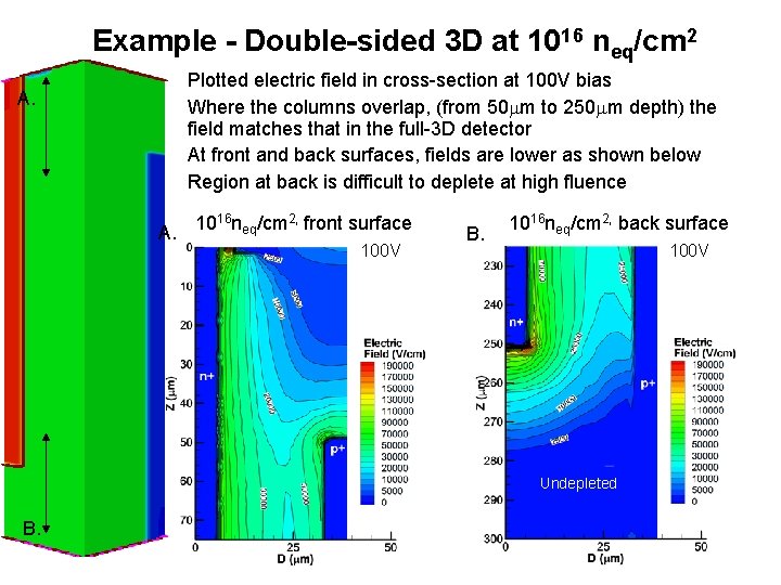
Example - Double-sided 3 D at 1016 neq/cm 2 A. • • Plotted electric field in cross-section at 100 V bias Where the columns overlap, (from 50 m to 250 m depth) the field matches that in the full-3 D detector At front and back surfaces, fields are lower as shown below Region at back is difficult to deplete at high fluence 16 n /cm 2, front surface 10 eq A. 100 V B. 1016 neq/cm 2, back surface 100 V Undepleted B.

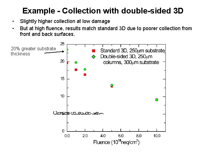
Example - Collection with double-sided 3 D • • Slightly higher collection at low damage But at high fluence, results match standard 3 D due to poorer collection from front and back surfaces. 20% greater substrate thickness

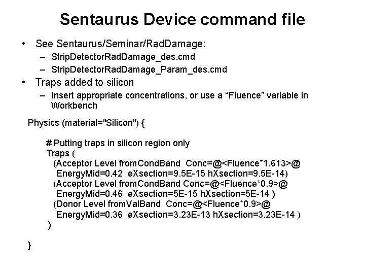
Sentaurus Device command file • See Sentaurus/Seminar/Rad. Damage: – Strip. Detector. Rad. Damage_des. cmd – Strip. Detector. Rad. Damage_Param_des. cmd • Traps added to silicon – Insert appropriate concentrations, or use a “Fluence” variable in Workbench Physics (material="Silicon") { # Putting traps in silicon region only Traps ( (Acceptor Level from. Cond. Band Conc=@<Fluence*1. 613>@ Energy. Mid=0. 42 e. Xsection=9. 5 E-15 h. Xsection=9. 5 E-14) (Acceptor Level from. Cond. Band Conc=@<Fluence*0. 9>@ Energy. Mid=0. 46 e. Xsection=5 E-15 h. Xsection=5 E-14 ) (Donor Level from. Val. Band Conc=@<Fluence*0. 9>@ Energy. Mid=0. 36 e. Xsection=3. 23 E-13 h. Xsection=3. 23 E-14 ) ) }

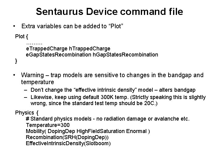
Sentaurus Device command file • Extra variables can be added to “Plot” Plot { ……… e. Trapped. Charge h. Trapped. Charge e. Gap. States. Recombination h. Gap. States. Recombination } • Warning – trap models are sensitive to changes in the bandgap and temperature – Don’t change the “effective intrinsic density” model – alters bandgap – Likewise, keep using default 300 K temp. (Strictly speaking this is slightly wrong, since the standard test temp should be 20 C. ) Physics { # Standard physics models - no radiation damage or avalanche etc. Temperature=300 Mobility( Doping. Dep High. Field. Saturation Enormal ) Recombination(SRH(Doping. Dep)) Effective. Intrinsic. Density(Slotboom)

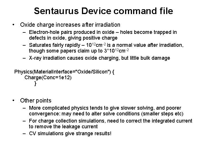
Sentaurus Device command file • Oxide charge increases after irradiation – Electron-hole pairs produced in oxide – holes become trapped in defects in oxide, giving positive charge – Saturates fairly rapidly – 1012 cm-2 is a normal value after irradiation, though some papers claim up to 3*1012 cm-2 – X-ray irradiation causes oxide charging, but little bulk damage Physics(Material. Interface="Oxide/Silicon") { Charge(Conc=1 e 12) } • Other points – More complicated physics tends to give slower solving, and poorer convergence: may need to alter solve conditions (smaller steps etc) – For charge collection simulations, need to correct the integrated current to remove the leakage current – CV simulations give strange results!

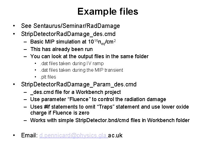
Example files • See Sentaurus/Seminar/Rad. Damage • Strip. Detector. Rad. Damage_des. cmd – Basic MIP simulation at 1015 neq/cm 2 – This has already been run – You can look at the output files in the same folder • . dat files taken during IV ramp • . dat files taken during the MIP transient • . plt files • Strip. Detector. Rad. Damage_Param_des. cmd – _des. cmd file for a Workbench project – Use parameter “Fluence” to control the radiation damage – Uses #if statements to omit “Traps” statement and use lower oxide charge if Fluence is zero – Works with simple Strip. Detector. bnd/cmd files in Workbench folder • Email: d. pennicard@physics. gla. ac. uk
