Radiation damage considerations in accelerator beam environments DAVID
 Ex-Aust.")
Radiation damage considerations in accelerator beam environments DAVID V WEBB Ph. D (ret’d) Ex-Aust. Radiation Protection & Nuclear Safety Agency Yallambie, Victoria, Australia


Overview • The impact of radiation upon equipment used on accelerator beam lines is a continuing concern. • Materials, cabling and instrumentation will experience aging and degradation and even failure • Damage depends on the nature of the radiation and the intensity of the fields. • This discussion will review • The fundamentals of radiation interactions • Damage mechanisms • Strategies to minimise or delay the effects of radiation damage
 Electrons, protons, etc. Ionizing Indirectly")
Classification of radiation Nonionizing Radiation Directly ionizing (charged particles) Electrons, protons, etc. Ionizing Indirectly ionizing (neutral particles) Photons, neutrons 4
 Characteristic Photon (γ or X-ray)")
Types of radiation Radiation (Eke = 1 Me. V) Characteristic Photon (γ or X-ray) Neutron Beta (β) or electron Proton Alpha (α) Ionization Indirect Direct Rest Mass (amu) -- 1. 008665 (940 Me. V) 0. 000548 (0. 511 Me. V) 1. 007276 (938 Me. V) 4. 0027 (3730 Me. V) Speed (rel. to c) 100% 4. 60% 94. 10% 4. 60% 2. 30% 82, 000 cm 39250 cm 319 cm 1. 81 cm 0. 56 cm Range in air* * range based on a 99. 9% reduction
: • •")
Radiation Processes • Excitation and ionization processes through interactions: • Photons (mainly): • • Photo-electric effect The Compton effect Pair and triplet production and positron annihilation Photo-nuclear effect • Electrons • Coulomb interaction with a charged particle • Atomic excitations • Bremsstrahlung (X-rays) • Protons • Coulomb interaction with a charged particle • Recoil ions • Nuclear reactions • Neutrons • Nuclear reactions • Recoil ions

Radiation Impurity Production Atomic Displacement Ionization Neutron Directly by absorption High energy neutrons reactions (mostly can cause thermal n's), also may displacements lead to more reactions Indirectly Alpha He buildup can cause May cause atomic pressurization problems displacement Causes sizeable ionization Proton Beta or e Photon H buildup, nuclear reactions Some displacement Yes Rare displacements (via Nuclear photoreactions Yes, indirectly Compton)

Macroscopic damage mechanisms • Transient Charge Generation - direct or indirect ionization • Structural Damage - displacement, scission • Impurities - nuclear reactions (e. g. secondary production by neutrons) Dose Effects Single Event Effects (SEEs) Dose Rate Effects

• In the case of electron accelerators producing electron or photon beams • Ionization effects will tend to dominate • If the energies are high enough, • secondary charged particles and neutrons created • cause atomic displacements and impurity production. • Scattered beam sources • Variable spectra and intensity

Z dependence Ge Si

Absorbed dose distributions • Photon beams • Inverse square • energy dependent dose maximum depth (zero up to 500 k. V) • Secondary electrons deposit dose • Electron beams • Coulomb interactions with orbital electrons and nuclei • Build-up of secondary electrons • Rapid fall off beyond dose maximum, highly scattered • Bremsstrahlung tail
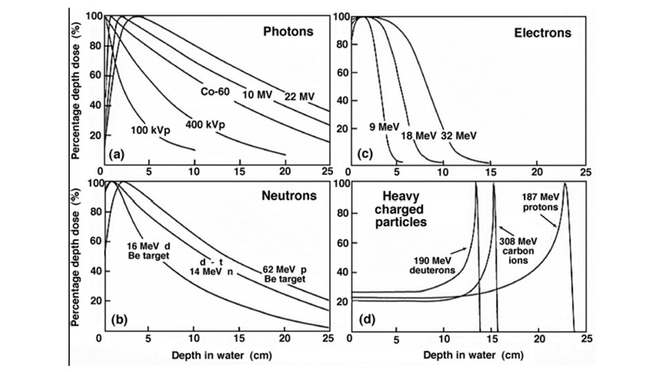

Absorbed dose distributions • Neutron fields • Produced by nuclear reactions • Photons/electrons > 8 -10 Me. V – max. yield from “giant” resonance ~20 Me. V • Release protons and heavier nuclei • Secondary charged particles deposit dose • 14 Me. V neutron beam similar depth-dose to 60 Co beam • Proton beams • Coulomb interactions with orbital electrons • Nuclear reactions • Bragg peak – distinct range
 units of e. V/cm; often called")
How much ionization? • Linear Energy Transfer (LET) units of e. V/cm; often called Stopping Power • LET is dependent on the particle, its energy and the material traversed LET proportional to z 2/E • Specific Ionization (pairs/cm) S. I. = LET/w (e. V/cm)/(e. V/ip) • w is the average Energy expended to create an (electron-hole) ion pair Material Air Si Ge Ga. As Si. O 2 w (e. V/ip) 34 3. 6 2. 8 4. 8 17

• Radiation tends to be increasingly damaging in the following order of molecular formation (largely due to the ability of ionization to disrupt the bonds) • Metallic bond (least damaged) • Ionic bond • Covalent bond (most damaged) • Since biological (organic) tissue is characterized by substantial covalent bonding, generally more susceptible to radiation damage than metallic-bonded structural components • Degradation of polymers by splitting molecules or causing branching is known as scission

Insulation damage • Cables – particularly coax, triax • Magnet windings

Neutrons from therapy treatment facilities • Therapy treatment heads have high Z materials • • Copper targets Tungsten collimators Steel filters Lead shielding • Neutron production • • • Produced by high-energy photons and electrons incident on these components. Threshold X-ray and electron energies > 10 Me. V, particularly > 18 Me. V (γ, n) reaction cross sections (probability 10 x (e, n) reactions) Bounce around until thermalise and are captured or decay. (n, γ), (n, p) reactions, activate linac head components, treatment table and patient. 17

Neutron damage to CCD devices • Due to their high sensitivity and signal-to-noise ratio, charge-coupled devices (CCDs) are widely used in CCTV cameras. However, a drawback is their extreme vulnerability to radiation. • While charged particle fields and photons, can create significant effects, neutrons are also effective due to their ability to produce knock-on charged particles and other nuclear interactions. • These effects include increased bulk dark current, surface dark current and inversion threshold voltage shifts. Results in increased pixel intensity.

Neutron damage to CCD CCTV cameras

Neutron damage to CCD devices • Traditional mitigation can be by shielding or increased separation. The latter is difficult in scattered neutron fields which can persist for some time (neutron t 1/2 ~ 10 minutes). • Techniques such as cooling and annealing are generally not feasible for commercial cameras. • Old technology such as Uvicon tubes are radiation resistant but less light sensitive (and usually black & white).

MLC alignment camera • Measures positioning of the leaves in a multi-leaf collimator • Uses Charge Injection Device (CID) technology • Less sensitive to radiation damage due to PMOS semiconductor structure (many CCDs use NMOS) • Differs from CCD in that charge is not transferred from a pixel on readout so readout is non-destructive • Peltier cooled to reduce dark currents • Failed after being in use for several years

Amorphous Silicon portal imager Artifact from damage to edge electronics

• For instrumentation, radiation damage can be divided into electromagnetic and bulk damage components. • Ionizing radiation such as X-rays, gammas, electrons and protons, create free charge in materials which affects properties and performance. • Neutrons, protons, alphas and pions (hadrons) can also produce bulk damage. • Detectors are sensitive to both but bulk effects are often more important.
 • Accumulated radiation exposures (poss. chronic) over time • Control")
Total Ionizing Dose (TID) • Accumulated radiation exposures (poss. chronic) over time • Control and detector components around particle accelerators can be exposed to up to 100 kilogray/year of absorbed dose (100 k. Gy = 10 Mrad) • Absorbed dose is in the oxides/insulators • Commercial integrated circuits can stand up to 100 Gy • Bipolar integrated circuits have higher tolerance than CMOS • Hardened circuits (SOI or SOS substrates) might withstand 10 k. Gy • Device parameters will shift as a function of dose • Parameter shifts are quasi-permanent

Semiconductor Detectors • Vulnerable to bulk damage due to large volumes and uniform crystalline structure (e. g. Ge. Li, HPGe) • Significant effect from heavy charged particles and neutrons • Normally minor effect from photons or electrons (minimum energy of 250 ke. V) • Common type is Frankel defect • atom displaced to an interstitial site • vacancy is a trapping site for charge carriers • Consequences are higher leakage current, degraded resolution

Radiation effects in electronics • Solid state electronics because of thin sensitive layers tend to be most sensitive to ionization and the associated accumulation of charge in the material. • Two mechanisms dominate • Lattice displacement - neutrons, protons, alpha particles and high energy photons/electrons • change arrangement of atoms in in the crystal lattice, create lasting damage and increase number of recombination centres • Depletes minority carriers, worsens analog properties of junctions • Ionization effects – primary and secondary charged particles down to low energies • Usually transient, creates glitches and soft errors • Can lead to destruction if other processes are triggered • Can include photo-current effects from X-rays and UV
 Lowest DOSE RATE gives highest degradation β =")
TID in Bipolar Transistors (200 Gy) Lowest DOSE RATE gives highest degradation β = Ic /Ib ; Ib~ Rsurface

CMOS technology • Layered structure widely used in modern high density electronics • Radiation creates electron-hole pairs at the silicon oxide layer that migrate at different rates. • Holes are trapped at the Si-Si. O 2 interface to generate shifts in operating thresholds. • PMOS and NMOS have different damage behaviour – holes in PMOS attracted to the gate rather than the channel.

Micro-electronics • Single event effects dominate • Usually caused by high-energy particles leaving an ionized track behind. • Mostly affects only digital devices • • • Upsets (SEU) – state changes in memory and register bits, often reversible Latchups (SEL) – CMOS devices, PNPN structures Transient electrostatic discharge (SET) – spurious signals Snapback – similar to SEL in N-channel MOS transistors - avalanches Burnout (SEB) – power MOSFETs Rupture (SEGR) – MOSFET gates
")
Mitigation by design • Physical • Insulating substrates, e. g. Silicon on Insulator (SOI) • Choice of wide band gap substrates, e. g. Si. C or Ga. N - reduces sensitivity to deep-level • • • defects, improves latchup tolerance. Bipolar ICs rather than CMOS Rewriteable, non-volatile memory, such as magneto-restive RAM SRAM rather DRAM Annular “edgeless” MOSFETS Buried isolation layers • Logical • Memory error correction • Redundancy at both circuit and system levels • Radiation hardened technology • Can have higher costs • Can impact performance

Evolution of technology • As the transistor feature size reduces, less charge required to cause state change • Single event effects become more significant • DRAM/SRAM particularly at risk BUT • Scaling can also reduce dose deposited, increased tolerance • Over a decade DRAM/SRAM bit sensitivity has reduced by possibly 2 orders of magnitude correlated with technology node size (currently at 22 nm as defined by the ITRS)

What else? • Instrument environment • Map scatter fields • Monte Carlo modelling - which code? • If photons/electrons – EGSnrc, Penelope, Geant 4, MCNPX ` • If protons – Geant 4/Topas, MCNPX, Fluka • If neutrons – MCNPX, Fluka, MORSE, Geant 4 (only for high energies) • Good example: Roesler et al, SLAC-PUB-8490 (2000) • Shielding • Choice of materials • Geometry • Replacement program • survival probabilities – difficult to assess, usually empirical • Maintenance contract

THANK YOU

Discharge of stored electrons from an e-beam incident on PMMA ~7 cm
- Slides: 34