Radiation analysis on COTS components for the next

- Slides: 24

Radiation analysis on COTS components for the next LHC generation Presenter: Pascal Oser Supervisor: Julien Mekki Group: EN/STI-ECE 10/09/2020 1

Content • Introduction • Radiation environment in the LHC • Radiation effects on electronics • Testing of COTS components • Testing results • Conclusion • Outlook 10/09/2020 Pascal Oser 2

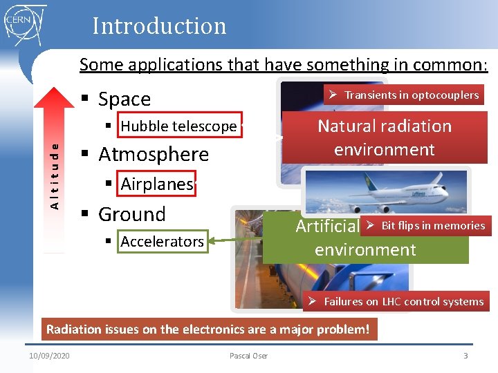
Introduction Some applications that have something in common: § Space Ø Transients in optocouplers Altitude § Hubble telescope § Atmosphere Natural radiation environment § Airplanes § Ground Ø Bit flips in memories Artificial radiation environment § Accelerators Ø Failures on LHC control systems Radiation issues on the electronics are a major problem! 10/09/2020 Pascal Oser 3

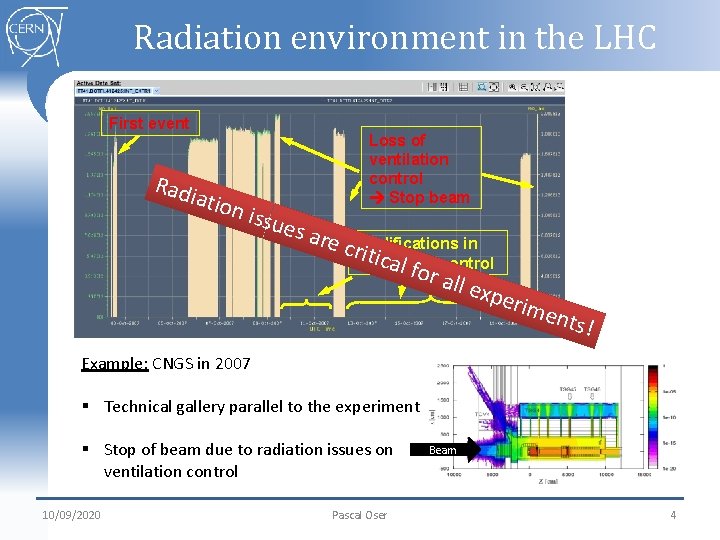
Radiation environment in the LHC First event Radi ation issu e Loss of ventilation control Stop beam s are in cr. Modifications iventilation tical control for all e xper im ents ! Example: CNGS in 2007 § Technical gallery parallel to the experiment § Stop of beam due to radiation issues on ventilation control 10/09/2020 Pascal Oser Beam 4

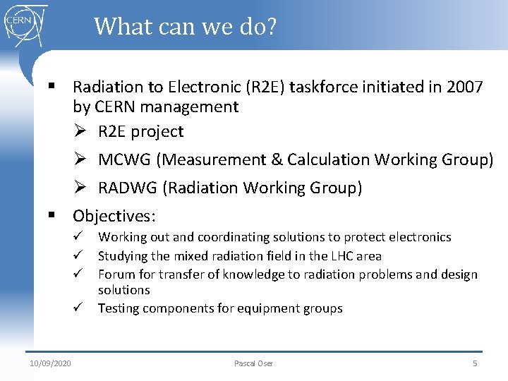
What can we do? § Radiation to Electronic (R 2 E) taskforce initiated in 2007 by CERN management Ø R 2 E project Ø MCWG (Measurement & Calculation Working Group) Ø RADWG (Radiation Working Group) § Objectives: ü Working out and coordinating solutions to protect electronics ü Studying the mixed radiation field in the LHC area ü Forum for transfer of knowledge to radiation problems and design solutions ü Testing components for equipment groups 10/09/2020 Pascal Oser 5

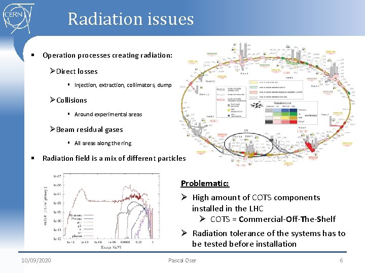
Radiation issues § Operation processes creating radiation: ØDirect losses § Injection, extraction, collimators, dump ØCollisions § Around experimental areas ØBeam residual gases § All areas along the ring § Radiation field is a mix of different particles Problematic: Ø High amount of COTS components installed in the LHC Ø COTS = Commercial-Off-The-Shelf Ø Radiation tolerance of the systems has to be tested before installation 10/09/2020 Pascal Oser 6

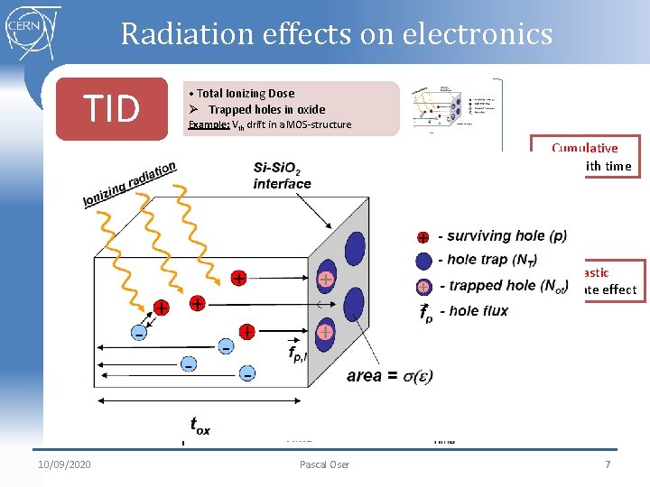
Radiation effects on electronics TID DD SEE 10/09/2020 • Total Ionizing Dose Ø Trapped holes in oxide Example: Vth drift in a MOS-structure Cumulative Effect with time • Displacement Damage Ø Vacancies in the structure Example: Increase of resistivity in Pin diodes • Single Event Effect Ø Induced pulse of charge in oxide Example: Bit Flip in memory Pascal Oser Stochastic Intermediate effect 7

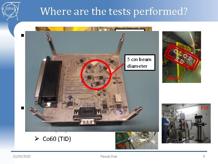
Where are the tests performed? Mixed field § Experimental areas (Inside CERN) Ø Radiation field similar to the LHC environment 5 cm beam diameter H 4 IRRAD CL O ED S CNRAD § Standard facilities (Outside CERN) PSI Ø PSI (TID, DD, SEE) PS-East. Area New! (After LS 1) Ø CEA (DD) Ø Co 60 (TID) 10/09/2020 CEA Pascal Oser 8

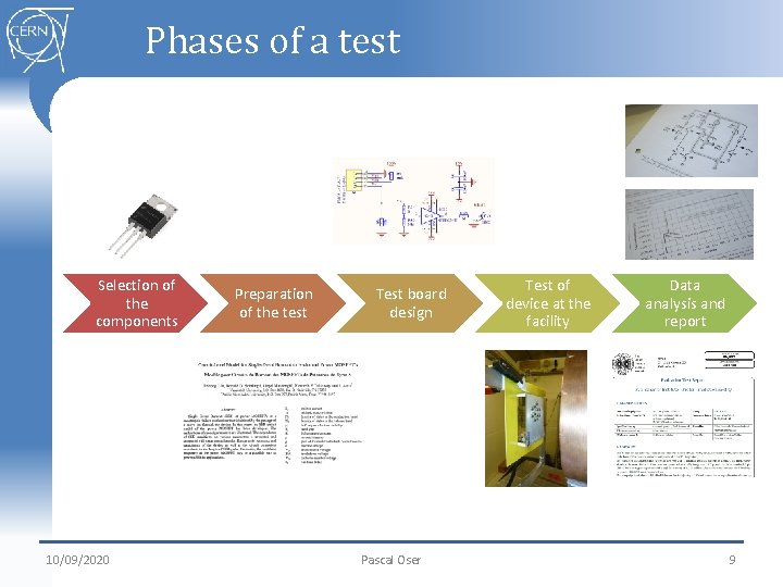
Phases of a test Selection of the components 10/09/2020 Preparation of the test Test board design Pascal Oser Test of device at the facility Data analysis and report 9

Results § SEE Ø Single Event Burnouts on Power Mos. FETs § TID Ø Bias effects on comparator inputs 10/09/2020 Pascal Oser 10

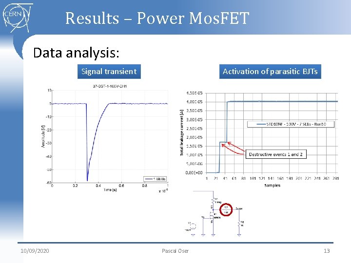
Results – Power Mos. FET Ø What is it? Device to switch high powers Range of 1 W to >1 KW Ø Problem: FETs susceptible to SEE Ø Type of SEE: Single Event Burnout (SEB) Crossing particle leads to overcurrent in the Power Mos. FET Ø Worst-case: 10/09/2020 Destructive event lead to melt down of the internal structure Pascal Oser 11

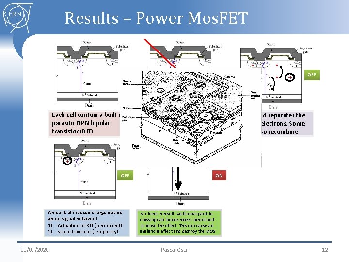
Results – Power Mos. FET OFF Each cell contain a built in parasitic NPN bipolar transistor (BJT) - + - + - + OFF - Particle cross through the device and leaves an ionization track behind + -+ OFF - Electric field separates the holes and electrons. Some of them also recombine - + OFF Amount of induced charge decide The hole in the base may about signal behavior! activate the BJT. Else it leaves 1) Activation of BJT (permanent) the device unharmed 2) Signal transient (temporary) 10/09/2020 + ON BJT feeds himself. Additional particle crossing can induce more current and increase the effect. This can cause an avalanche effect and destroy the MOS Pascal Oser 12

Results – Power Mos. FET Data analysis: Signal transient 10/09/2020 Activation of parasitic BJTs Pascal Oser 13

Results – Power Mos. FET 10/09/2020 Pascal Oser 14

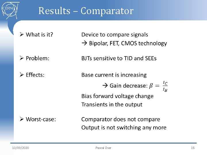
Results – Comparator 10/09/2020 Pascal Oser 15

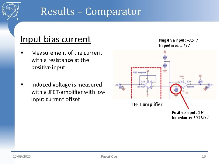
Results – Comparator Input bias current Negative input: +7. 5 V Impedance: 5 k § Measurement of the current with a resistance at the positive input § Induced voltage is measured with a JFET-amplifier with low input current offset JFET amplifier Positive input: 0 V Impedance: 100 M 10/09/2020 Pascal Oser 16

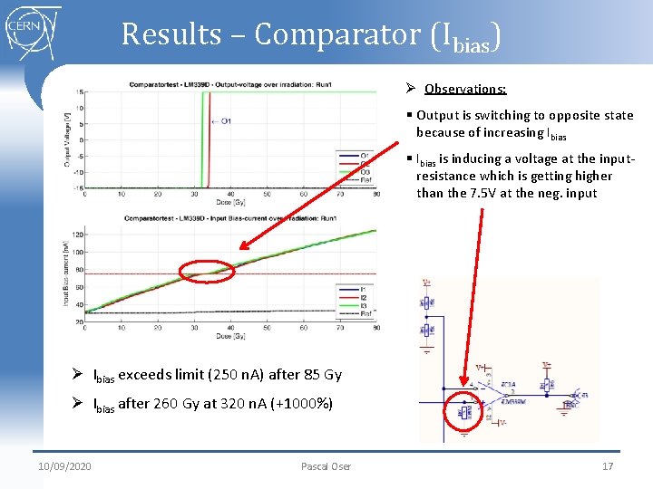
Results – Comparator (Ibias) Ø Observations: § Output is switching to opposite state because of increasing Ibias § Ibias is inducing a voltage at the inputresistance which is getting higher than the 7. 5 V at the neg. input Ø Ibias exceeds limit (250 n. A) after 85 Gy Ø Ibias after 260 Gy at 320 n. A (+1000%) 10/09/2020 Pascal Oser 17

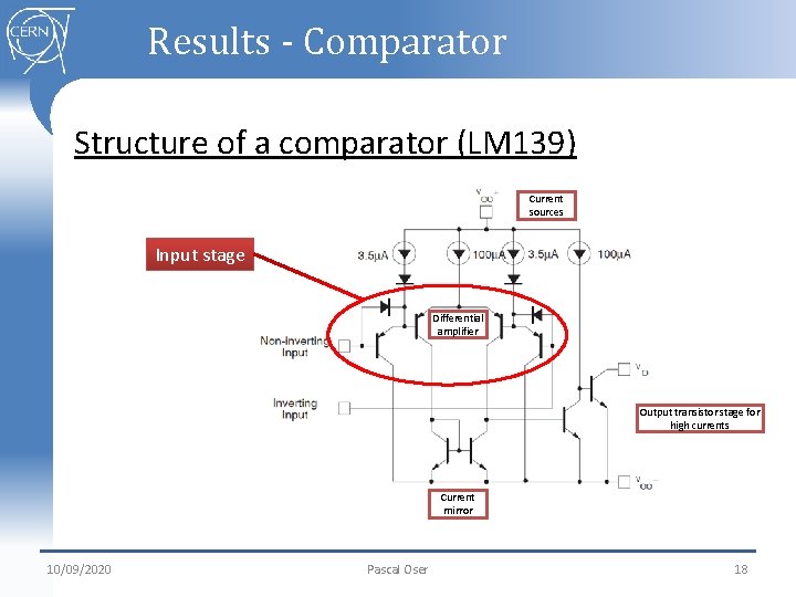
Results - Comparator Structure of a comparator (LM 139) Current sources Input stage Differential amplifier Output transistor stage for high currents Current mirror 10/09/2020 Pascal Oser 18

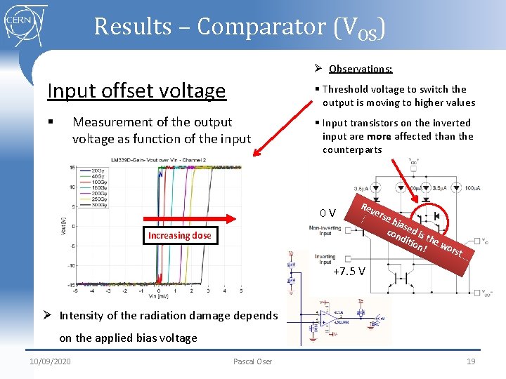
Results – Comparator (VOS) Ø Observations: Input offset voltage § Threshold voltage to switch the output is moving to higher values Measurement of the output voltage as function of the input § § Input transistors on the inverted input are more affected than the counterparts 0 V Rev e Increasing dose rse bia s con ed is diti the on! wo r st +7. 5 V Ø Intensity of the radiation damage depends on the applied bias voltage 10/09/2020 Pascal Oser 19

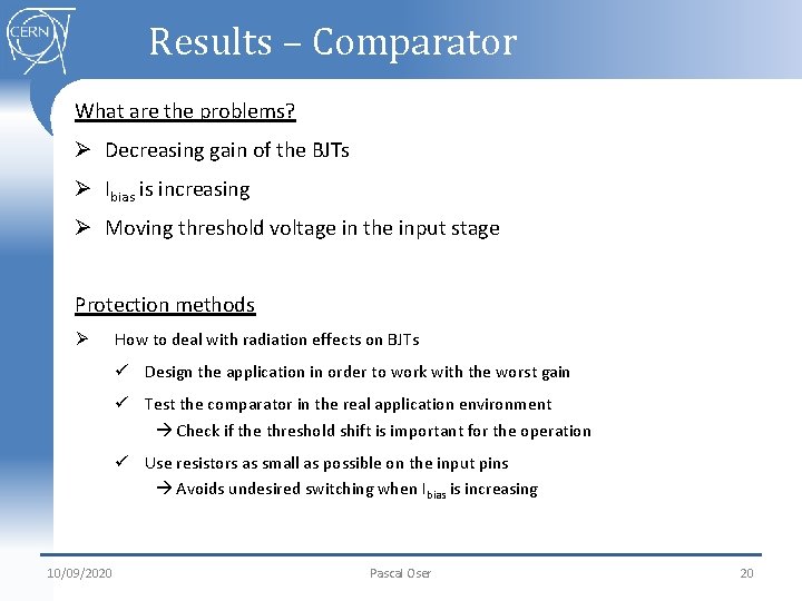
Results – Comparator What are the problems? Ø Decreasing gain of the BJTs Ø Ibias is increasing Ø Moving threshold voltage in the input stage Protection methods Ø How to deal with radiation effects on BJTs ü Design the application in order to work with the worst gain ü Test the comparator in the real application environment Check if the threshold shift is important for the operation ü Use resistors as small as possible on the input pins Avoids undesired switching when Ibias is increasing 10/09/2020 Pascal Oser 20

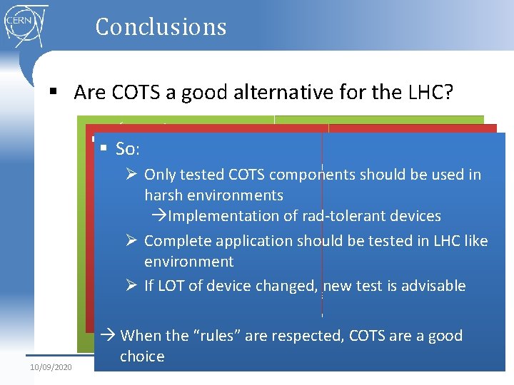
Conclusions § Are COTS a good alternative for the LHC? ü Yes! §§But! So: Ø Depending on the technology, good radiation 10/09/2020 ØØSingle event effects are a serious problem tolerance Only tested COTS components should be used in Stochastic effect Øharsh environments Cheaper & good availability within 20 years ØØ COTS are black boxes Dose not higher than a few hundreds Gy Implementation of rad-tolerant devices Ø (worst case); dose rate low in most LHC Internal design depends on: Manufacturer, production, Ø Complete application should be tested in LHC like package, LOT, etc. regions Time to react environment ØØ Radiation level of next LHC generation higher Experience of the concerned teams at a good ØØ If LOT of device changed, new test is advisable More critical luminosity, energies, bunch spacing, etc. level Radiation levels to be checked: Simulation + Monitoring Is improving more and more! When the “rules” are respected, COTS are a good choice Pascal Oser 21

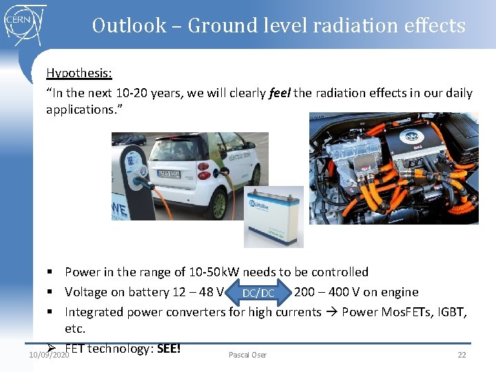
Outlook – Ground level radiation effects Hypothesis: “In the next 10 -20 years, we will clearly feel the radiation effects in our daily applications. ” § Power in the range of 10 -50 k. W needs to be controlled § Voltage on battery 12 – 48 V DC/DC 200 – 400 V on engine § Integrated power converters for high currents Power Mos. FETs, IGBT, etc. Ø FET technology: SEE! 10/09/2020 Pascal Oser 22

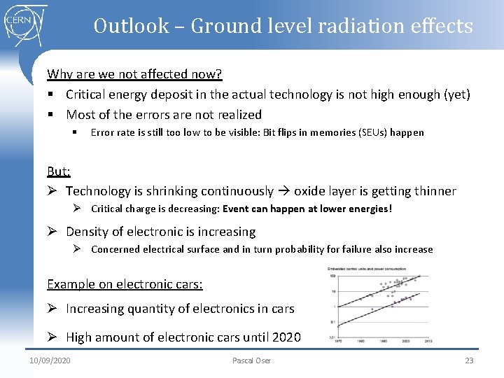
Outlook – Ground level radiation effects Why are we not affected now? § Critical energy deposit in the actual technology is not high enough (yet) § Most of the errors are not realized § Error rate is still too low to be visible: Bit flips in memories (SEUs) happen But: Ø Technology is shrinking continuously oxide layer is getting thinner Ø Critical charge is decreasing: Event can happen at lower energies! Ø Density of electronic is increasing Ø Concerned electrical surface and in turn probability for failure also increase Example on electronic cars: Ø Increasing quantity of electronics in cars Ø High amount of electronic cars until 2020 10/09/2020 Pascal Oser 23

End Thank you for your attention! Questions? 10/09/2020 Pascal Oser 24