Radar Interface Design Project Final Presentation Sponsor Scott




- Slides: 41

Radar Interface Design Project Final Presentation Sponsor: Scott Faulkner, Lockheed Martin Group #1 Catherine Donoso Diego Rocha Keith Weston

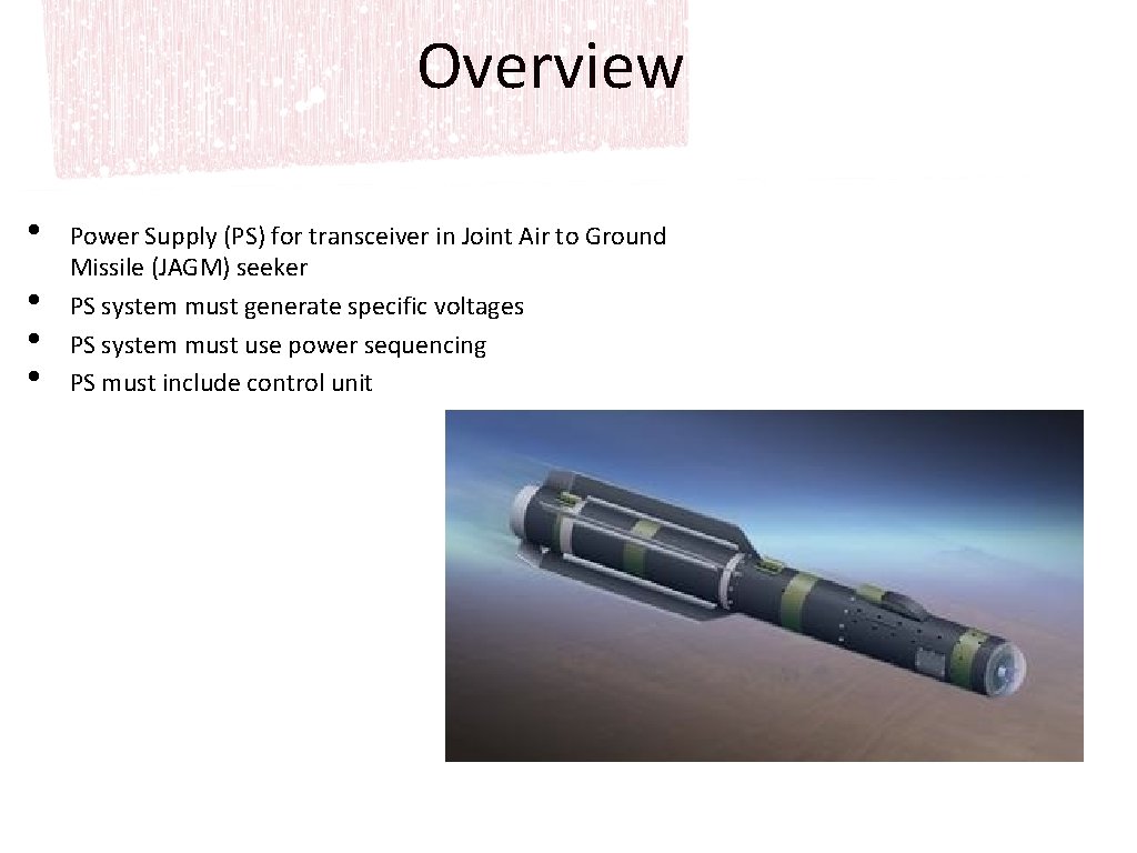
Overview • • Power Supply (PS) for transceiver in Joint Air to Ground Missile (JAGM) seeker PS system must generate specific voltages PS system must use power sequencing PS must include control unit

Goals • Lowest heat dissipation possible when selecting parts • limited airflow • No heat sink available directly on board, only for system • Less surface area on the board • • • Update design to utilize new technology Non-Rohs Compliant Military Grade Temperatures , -55° to +125° Celcius

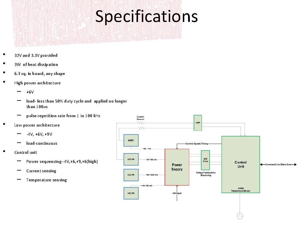
Specifications • • • 32 V and 3. 3 V provided 3 W of heat dissipation 6. 3 sq. in board, any shape High power architecture – – +6 V – pulse repetition rate from 1 to 100 k. Hz Low power architecture – – • load- less than 50% duty cycle and applied no longer than 100 us -4 V, +6 V, +9 V load-continuous Control unit – – – Power sequencing--4 V, +6, +9, +6(high) Current sensing Temperature sensing

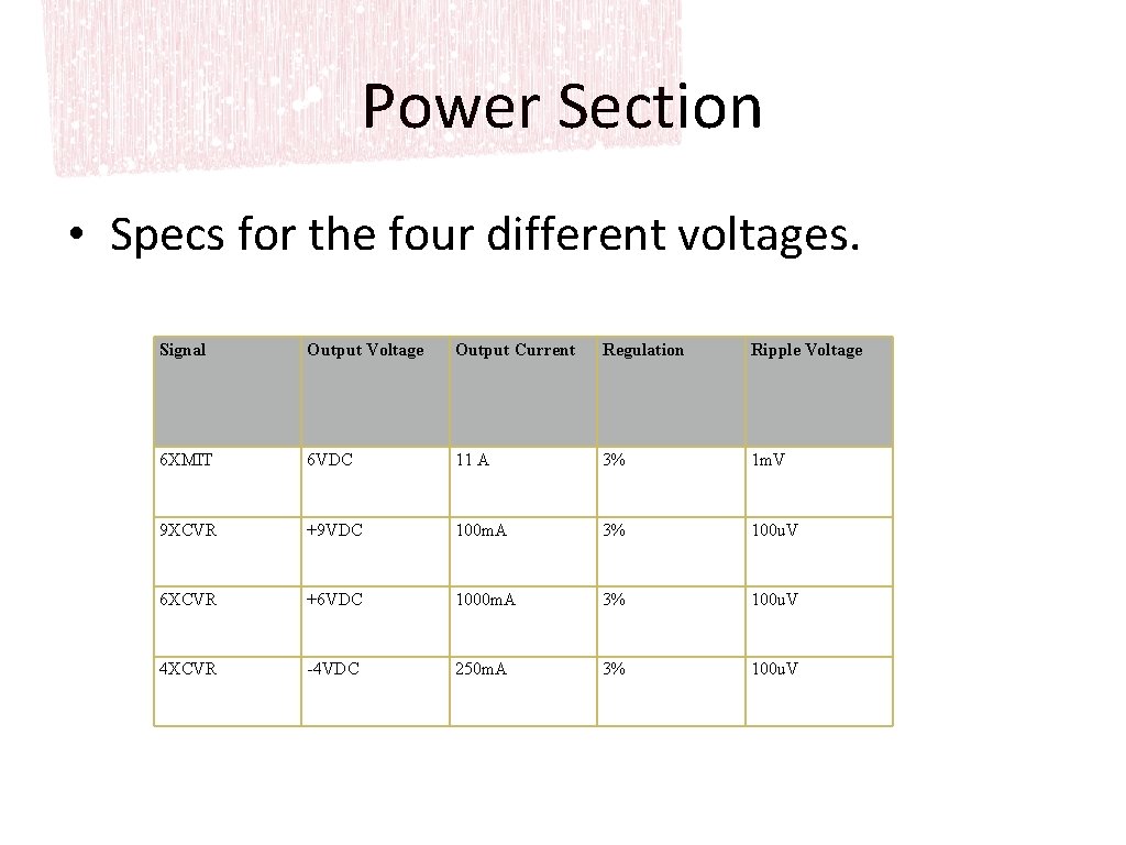
Power Section • Specs for the four different voltages. Signal Output Voltage Output Current Regulation Ripple Voltage 6 XMIT 6 VDC 11 A 3% 1 m. V 9 XCVR +9 VDC 100 m. A 3% 100 u. V 6 XCVR +6 VDC 1000 m. A 3% 100 u. V 4 XCVR -4 VDC 250 m. A 3% 100 u. V

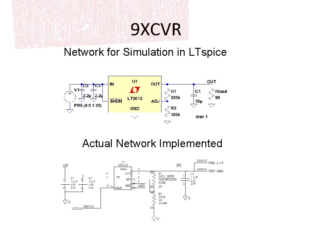
9 XCVR Network for Simulation in LTspice Actual Network Implemented

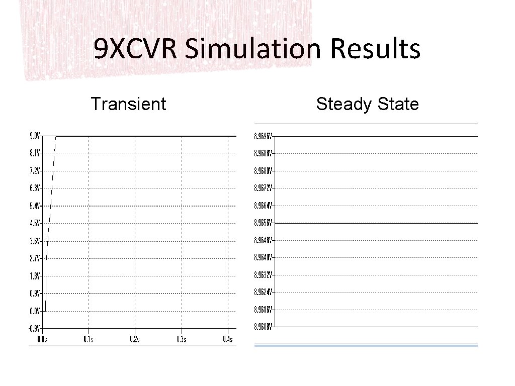
9 XCVR Simulation Results Transient Steady State

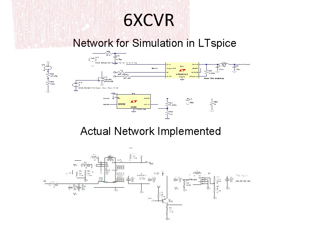
6 XCVR Network for Simulation in LTspice Actual Network Implemented

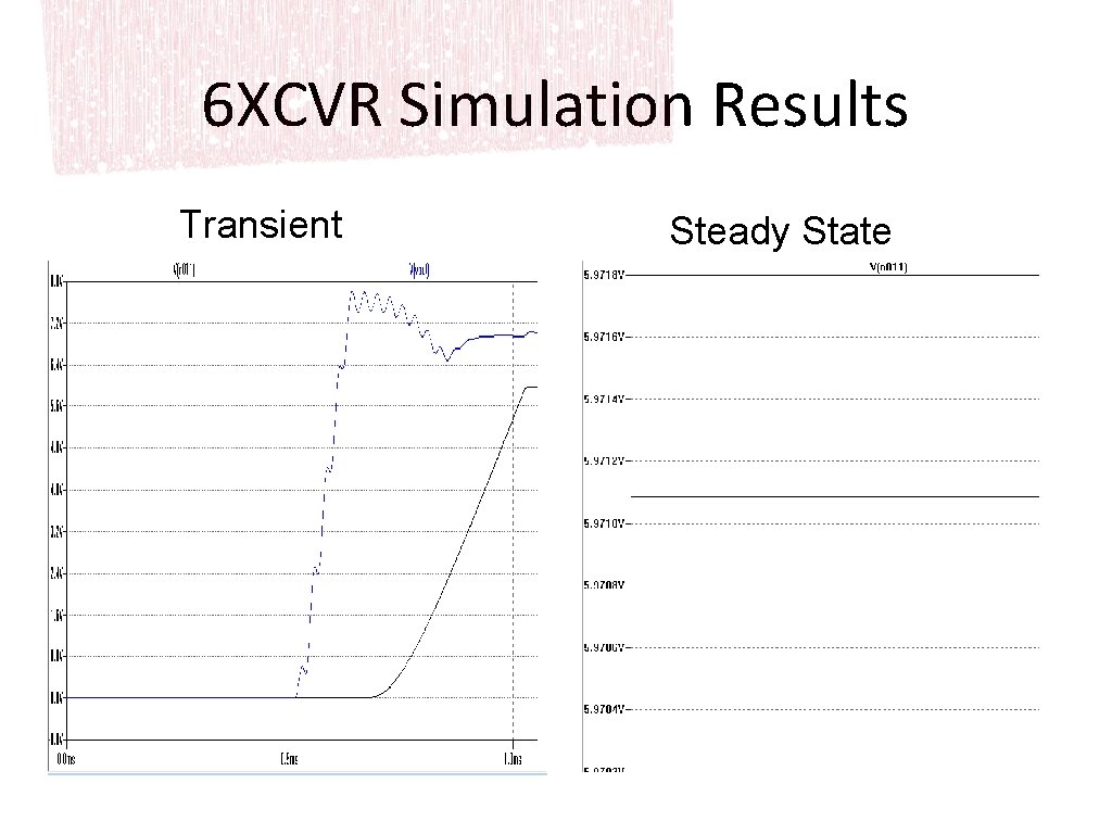
6 XCVR Simulation Results Transient Steady State

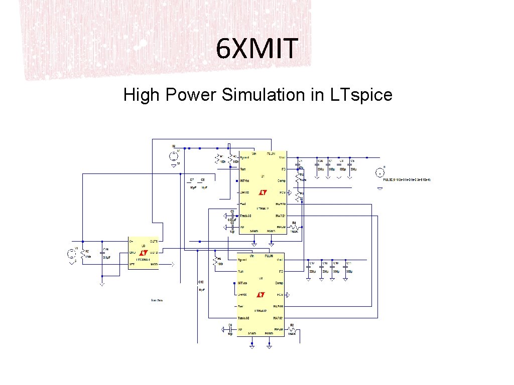
6 XMIT High Power Simulation in LTspice

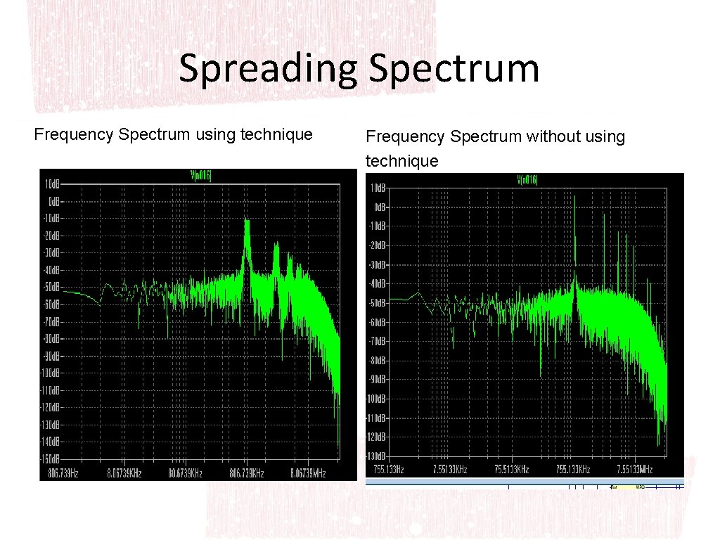
Spreading Spectrum Frequency Spectrum using technique Frequency Spectrum without using technique

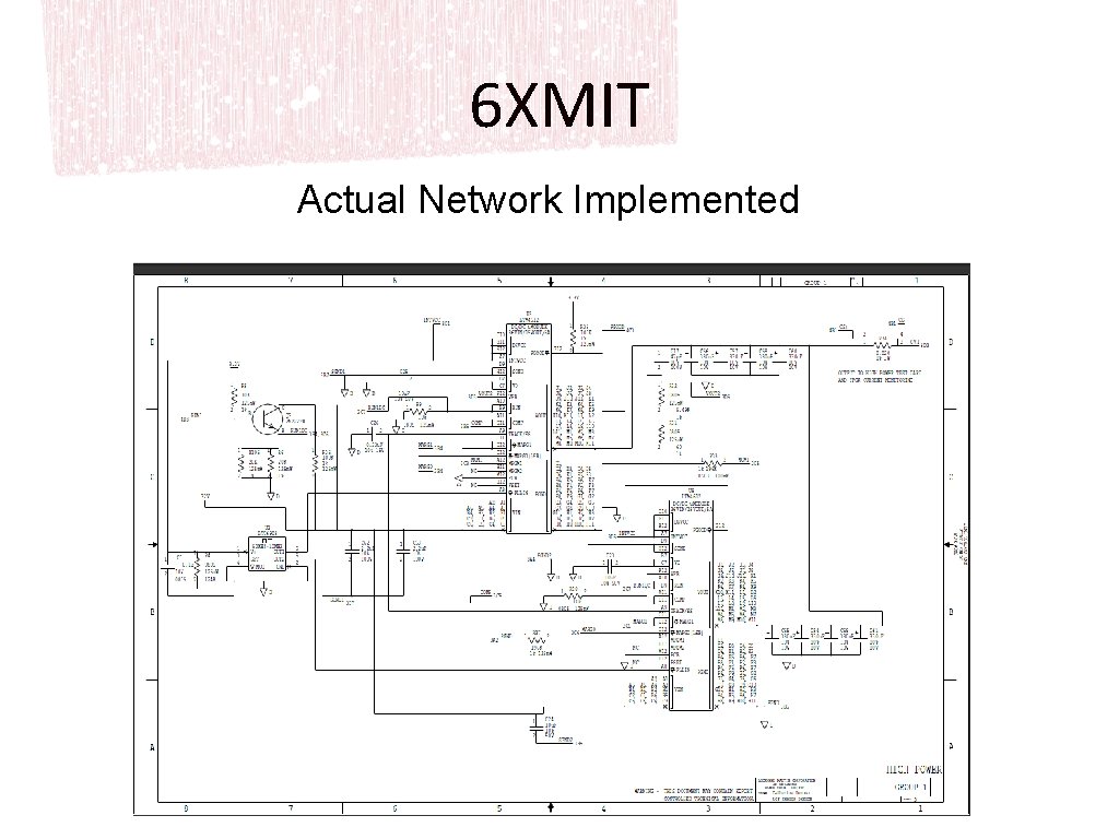
6 XMIT Actual Network Implemented

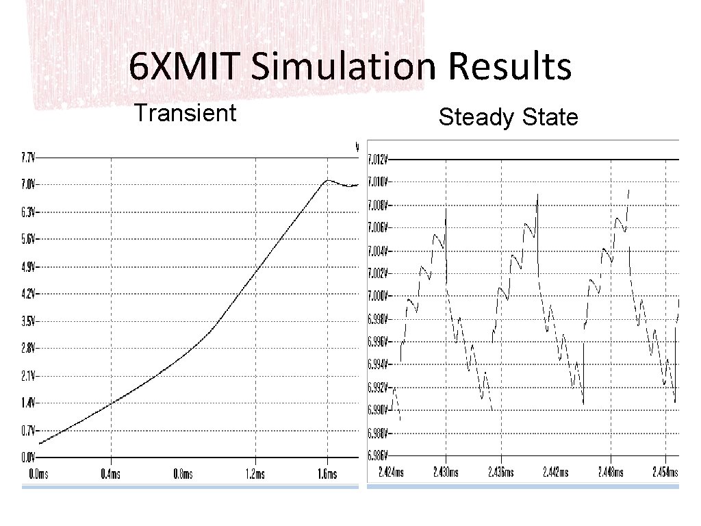
6 XMIT Simulation Results Transient Steady State

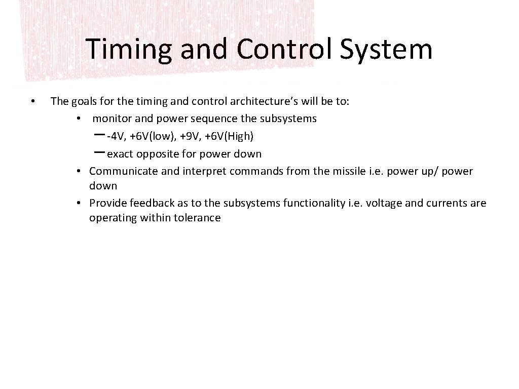
Timing and Control System • The goals for the timing and control architecture’s will be to: • monitor and power sequence the subsystems – -4 V, +6 V(low), +9 V, +6 V(High) – exact opposite for power down • Communicate and interpret commands from the missile i. e. power up/ power down • Provide feedback as to the subsystems functionality i. e. voltage and currents are operating within tolerance

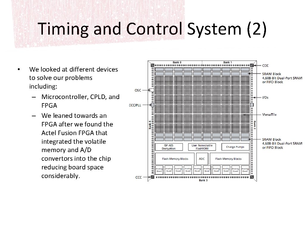
Timing and Control System (2) • We looked at different devices to solve our problems including: – Microcontroller, CPLD, and FPGA – We leaned towards an FPGA after we found the Actel Fusion FPGA that integrated the volatile memory and A/D convertors into the chip reducing board space considerably.

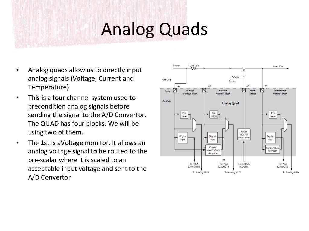
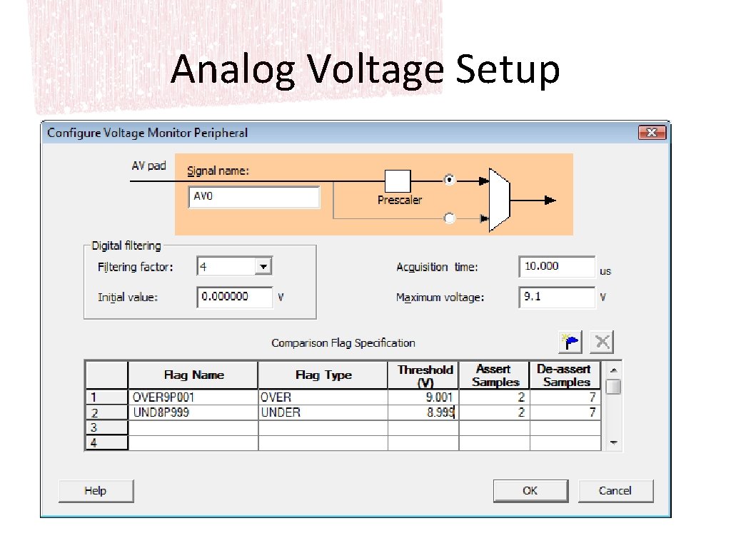
Analog Quads • • • Analog quads allow us to directly input analog signals (Voltage, Current and Temperature) This is a four channel system used to precondition analog signals before sending the signal to the A/D Convertor. The QUAD has four blocks. We will be using two of them. The 1 st is a. Voltage monitor. It allows an analog voltage signal to be routed to the pre-scalar where it is scaled to an acceptable input voltage and sent to the A/D Convertor

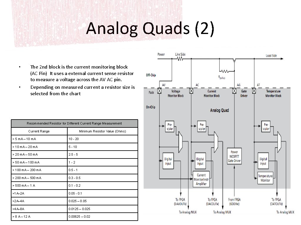
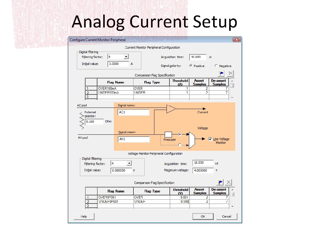
Analog Quads (2) • • The 2 nd block is the current monitoring block (AC Pin) It uses a external current sense resistor to measure a voltage across the AV AC pin. Depending on measured current a resistor size is selected from the chart Recommended Resistor for Different Current Range Measurement Current Range Minimum Resistor Value (Ohms) > 5 m. A – 10 m. A 10 - 20 > 10 m. A – 20 m. A 5 - 10 > 20 m. A – 50 m. A 2. 5 - 5 > 50 m. A – 100 m. A 1 -2 > 100 m. A – 200 m. A 0. 5 - 1 > 200 m. A – 500 m. A 0. 3 - 0. 5 > 500 m. A – 1 A 0. 1 - 0. 2 >1 A– 2 A 0. 05 - 0. 1 >2 A– 4 A 0. 025 – 0. 05 >4 A– 8 A 0. 0125 – 0. 025 > 8 A – 12 A 0. 00625 – 0. 02

Software Development Environment • • • ACTEL FUSION STARTER-KIT was used for software development Same exact FPGA model and die as used in our project which eliminated pin differences problems Onboard circuitry and software highlighted boards strengths.

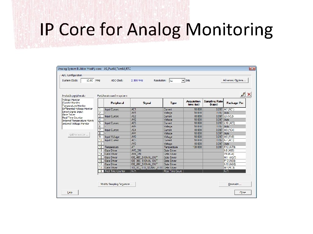
Software Development • Actel Libero IDE 8. 6 Advantages • Many implemented design ideas and tutorials available for download • Many IP Cores had graphical interface which made designing modules easier

IP Core for Analog Monitoring

Analog Voltage Setup

Analog Current Setup

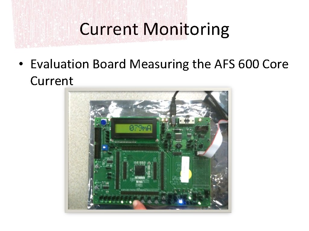
Current Monitoring • Evaluation Board Measuring the AFS 600 Core Current

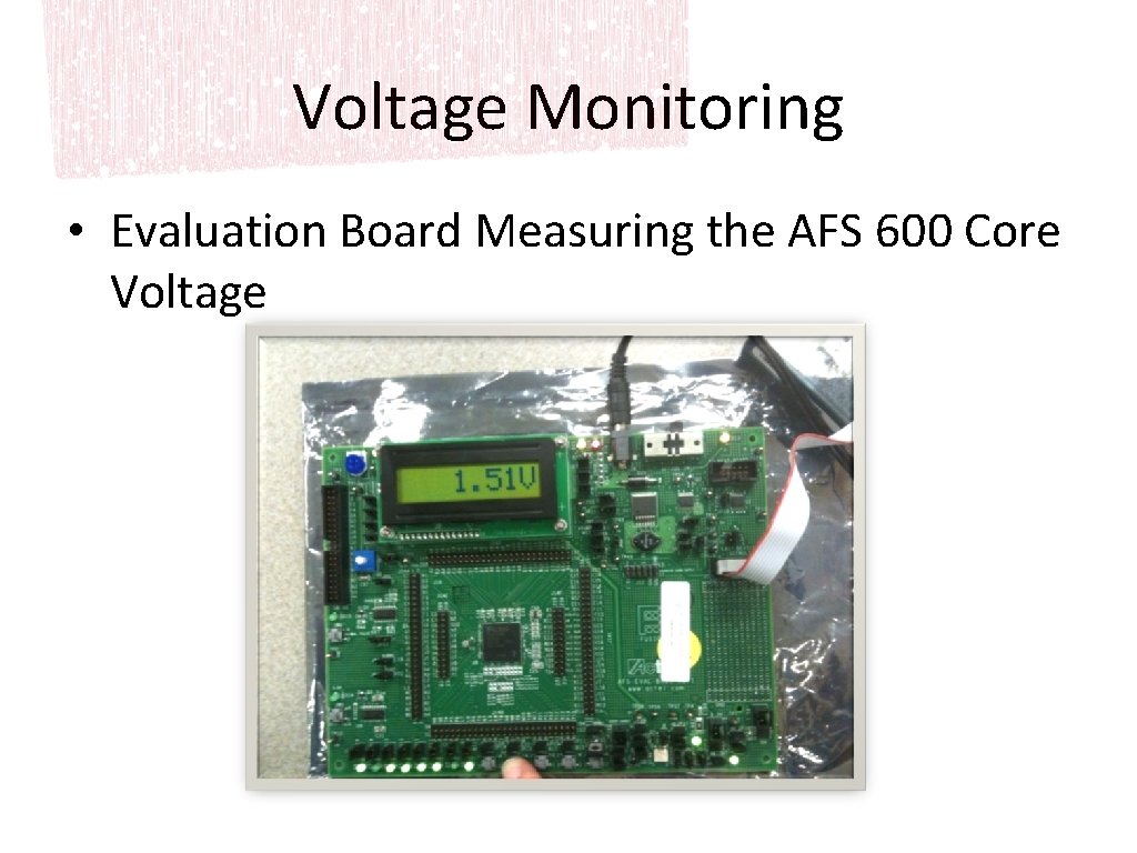
Voltage Monitoring • Evaluation Board Measuring the AFS 600 Core Voltage

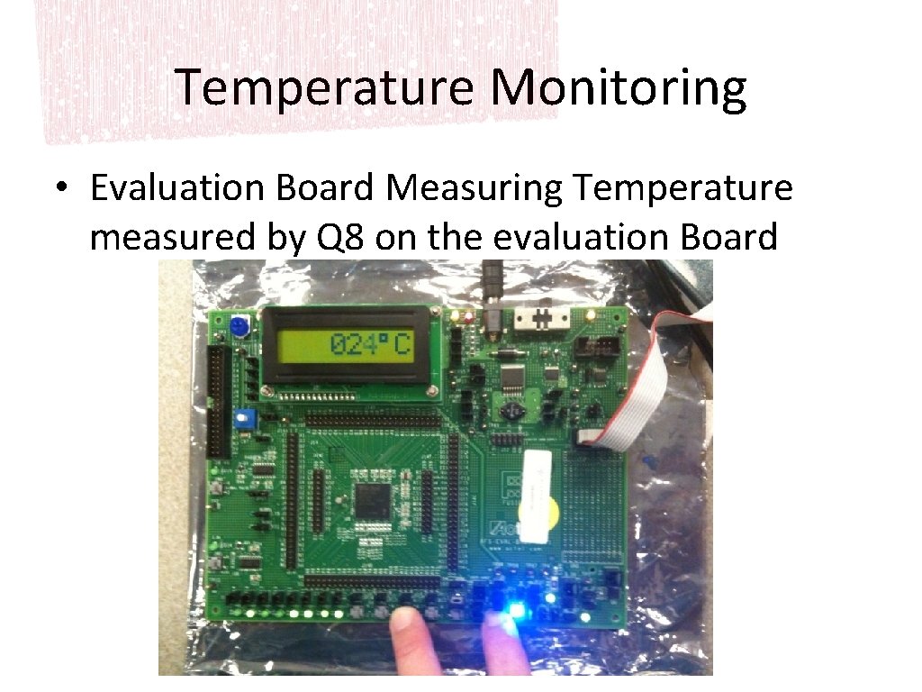
Temperature Monitoring • Evaluation Board Measuring Temperature measured by Q 8 on the evaluation Board

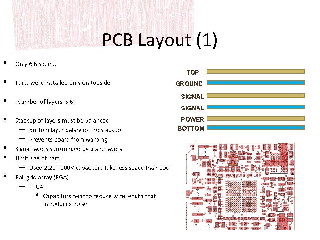
PCB Layout (1) • Only 6. 6 sq. in. , TOP • Parts were installed only on topside • Number of layers is 6 • • GROUND SIGNAL POWER Stackup of layers must be balanced BOTTOM – Bottom layer balances the stackup – Prevents board from warping Signal layers surrounded by plane layers Limit size of part – Used 2. 2 u. F 100 V capacitors take less space than 10 u. F Ball grid array (BGA) – FPGA • Capacitors near to reduce wire length that introduces noise

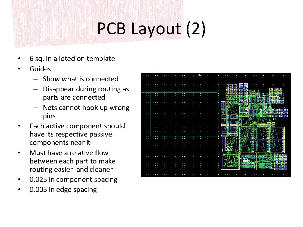
PCB Layout (2) • • • 6 sq. in alloted on template Guides – Show what is connected – Disappear during routing as parts are connected – Nets cannot hook up wrong pins Each active component should have its respective passive components near it Must have a relative flow between each part to make routing easier and cleaner 0. 025 in component spacing 0. 005 in edge spacing

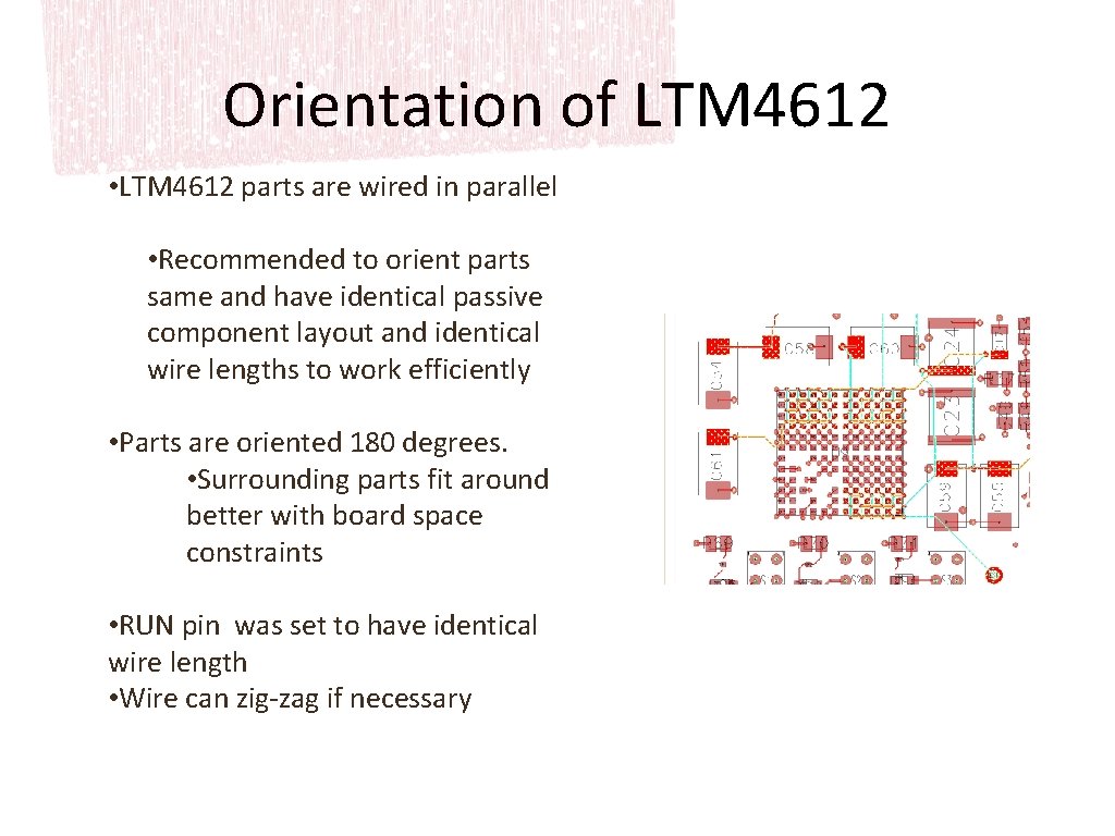
Orientation of LTM 4612 • LTM 4612 parts are wired in parallel • Recommended to orient parts same and have identical passive component layout and identical wire lengths to work efficiently • Parts are oriented 180 degrees. • Surrounding parts fit around better with board space constraints • RUN pin was set to have identical wire length • Wire can zig-zag if necessary

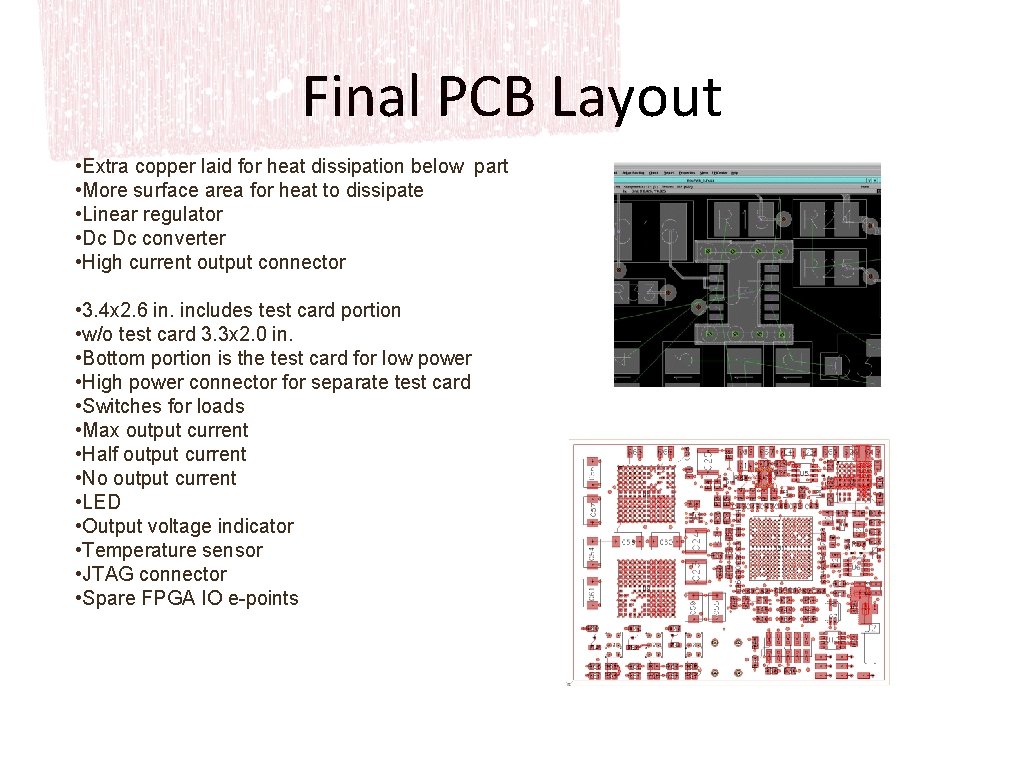
Final PCB Layout • Extra copper laid for heat dissipation below part • More surface area for heat to dissipate • Linear regulator • Dc Dc converter • High current output connector • 3. 4 x 2. 6 in. includes test card portion • w/o test card 3. 3 x 2. 0 in. • Bottom portion is the test card for low power • High power connector for separate test card • Switches for loads • Max output current • Half output current • No output current • LED • Output voltage indicator • Temperature sensor • JTAG connector • Spare FPGA IO e-points

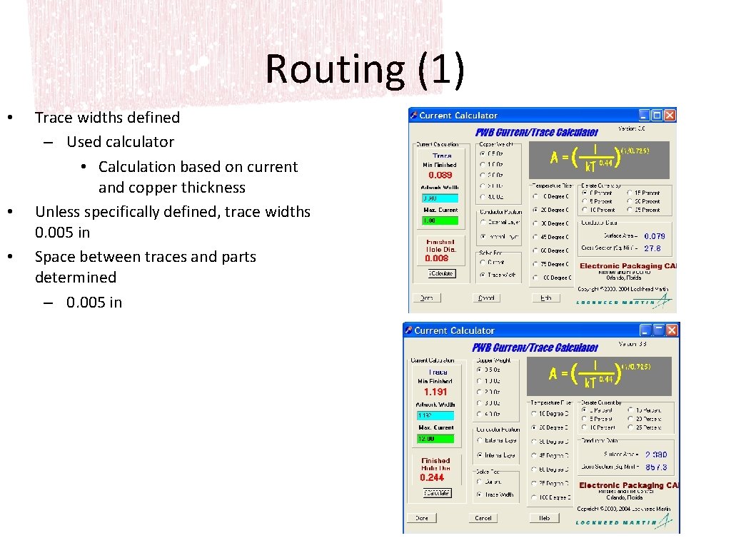
Routing (1) • • • Trace widths defined – Used calculator • Calculation based on current and copper thickness Unless specifically defined, trace widths 0. 005 in Space between traces and parts determined – 0. 005 in

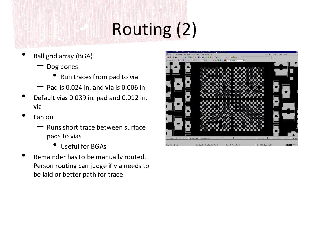
Routing (2) • • Ball grid array (BGA) – Dog bones • Run traces from pad to via – Pad is 0. 024 in. and via is 0. 006 in. Default vias 0. 039 in. pad and 0. 012 in. via Fan out – Runs short trace between surface pads to vias • Useful for BGAs Remainder has to be manually routed. Person routing can judge if via needs to be laid or better path for trace

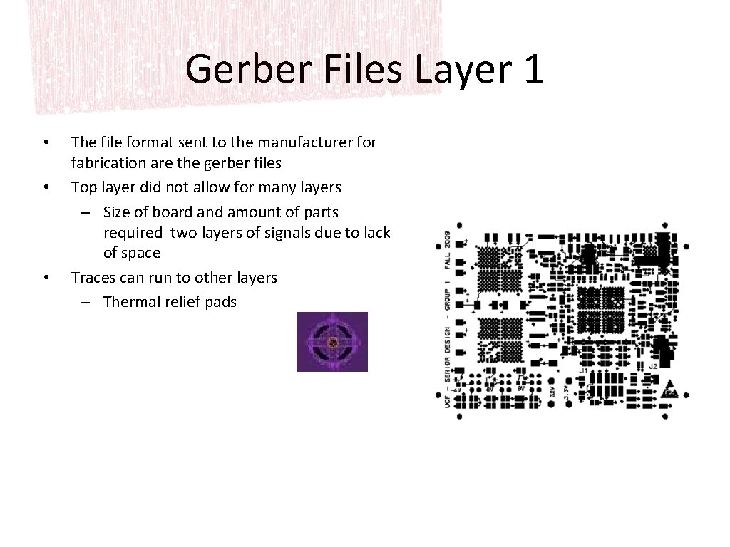
Gerber Files Layer 1 • • • The file format sent to the manufacturer for fabrication are the gerber files Top layer did not allow for many layers – Size of board and amount of parts required two layers of signals due to lack of space Traces can run to other layers – Thermal relief pads

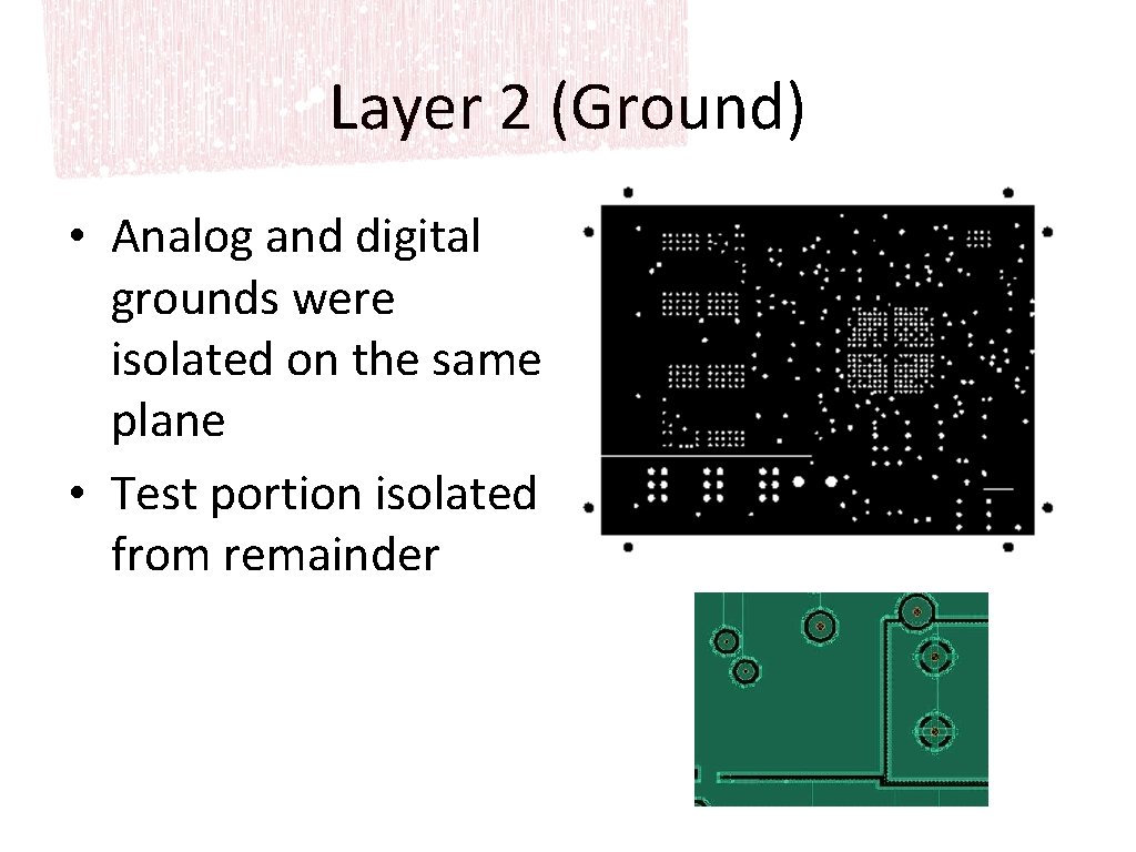
Layer 2 (Ground) • Analog and digital grounds were isolated on the same plane • Test portion isolated from remainder

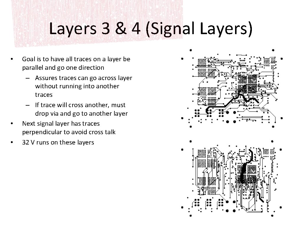
Layers 3 & 4 (Signal Layers) • • • Goal is to have all traces on a layer be parallel and go one direction – Assures traces can go across layer without running into another traces – If trace will cross another, must drop via and go to another layer Next signal layer has traces perpendicular to avoid cross talk 32 V runs on these layers

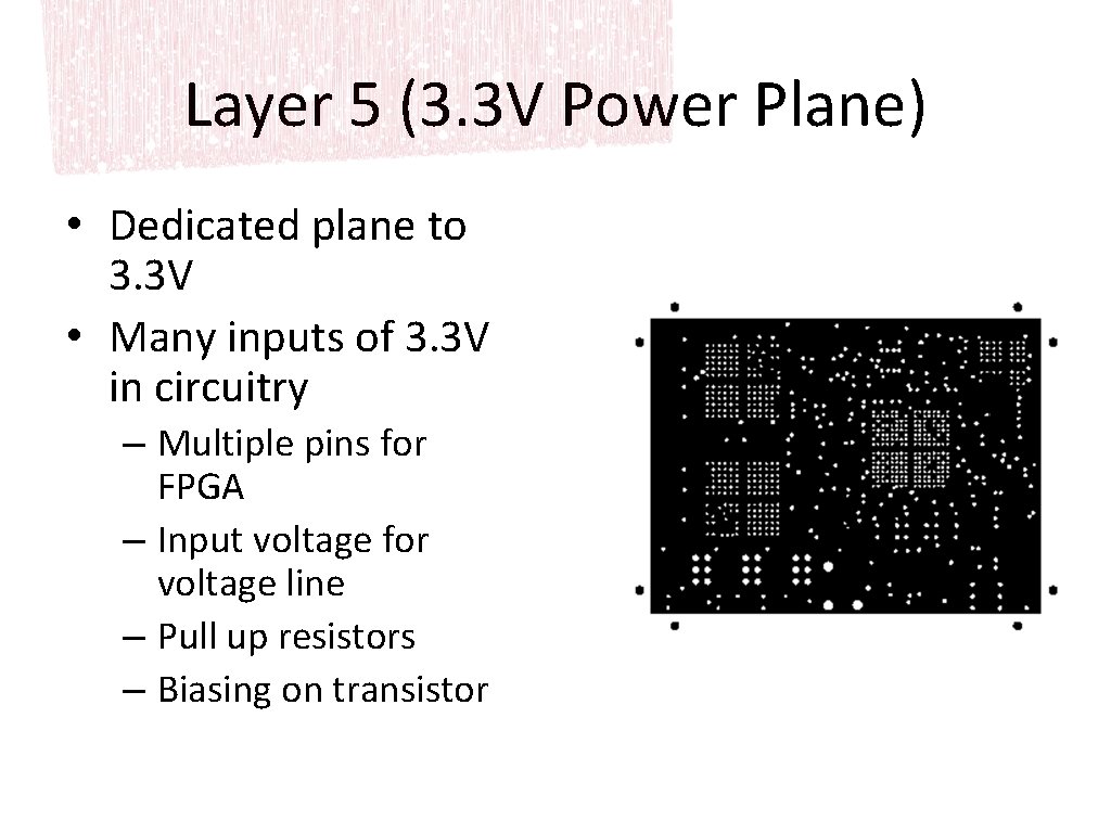
Layer 5 (3. 3 V Power Plane) • Dedicated plane to 3. 3 V • Many inputs of 3. 3 V in circuitry – Multiple pins for FPGA – Input voltage for voltage line – Pull up resistors – Biasing on transistor

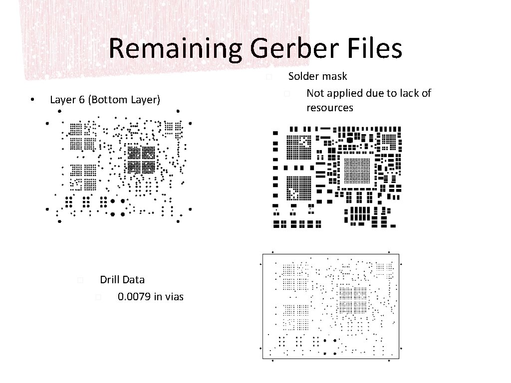
Remaining Gerber Files • Layer 6 (Bottom Layer) Drill Data 0. 0079 in vias Solder mask Not applied due to lack of resources

Fabrication • In-house fabrication • Available PCB manufacturers supported max. 6 layers – Wanted the flexibility if more layers were needed • Used 0. 5 oz. copper • Used chemical etching • Fiberglass used for dielectric between each layer • Impedance test not conducted

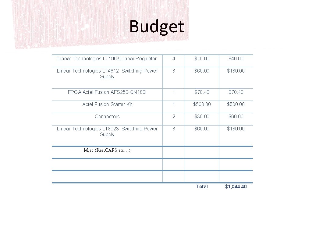
Budget Linear Technologies LT 1963 Linear Regulator 4 $10. 00 $40. 00 Linear Technologies LT 4612 Switching Power Supply 3 $60. 00 $180. 00 FPGA Actel Fusion AFS 250 -QN 180 I 1 $70. 40 Actel Fusion Starter Kit 1 $500. 00 Connectors 2 $30. 00 $60. 00 Linear Technologies LT 8023 Switching Power Supply 3 $60. 00 $180. 00 Total $1, 044. 40 Misc (Res, CAPS etc…)

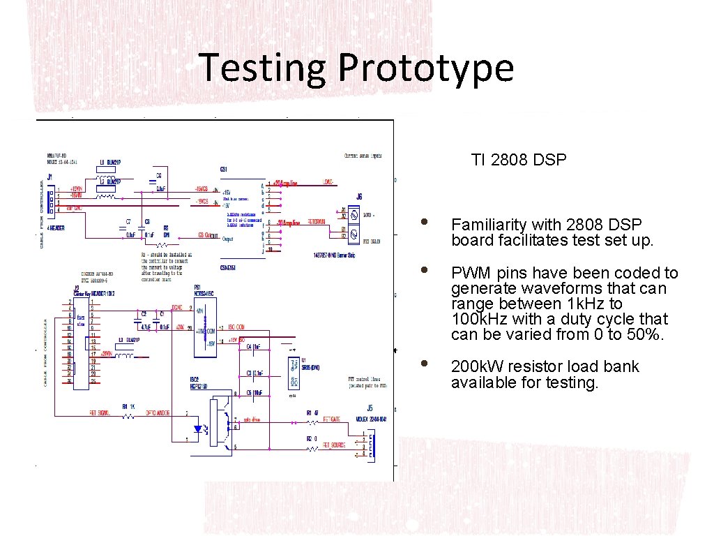
Testing Prototype TI 2808 DSP • • • Familiarity with 2808 DSP board facilitates test set up. PWM pins have been coded to generate waveforms that can range between 1 k. Hz to 100 k. Hz with a duty cycle that can be varied from 0 to 50%. 200 k. W resistor load bank available for testing.

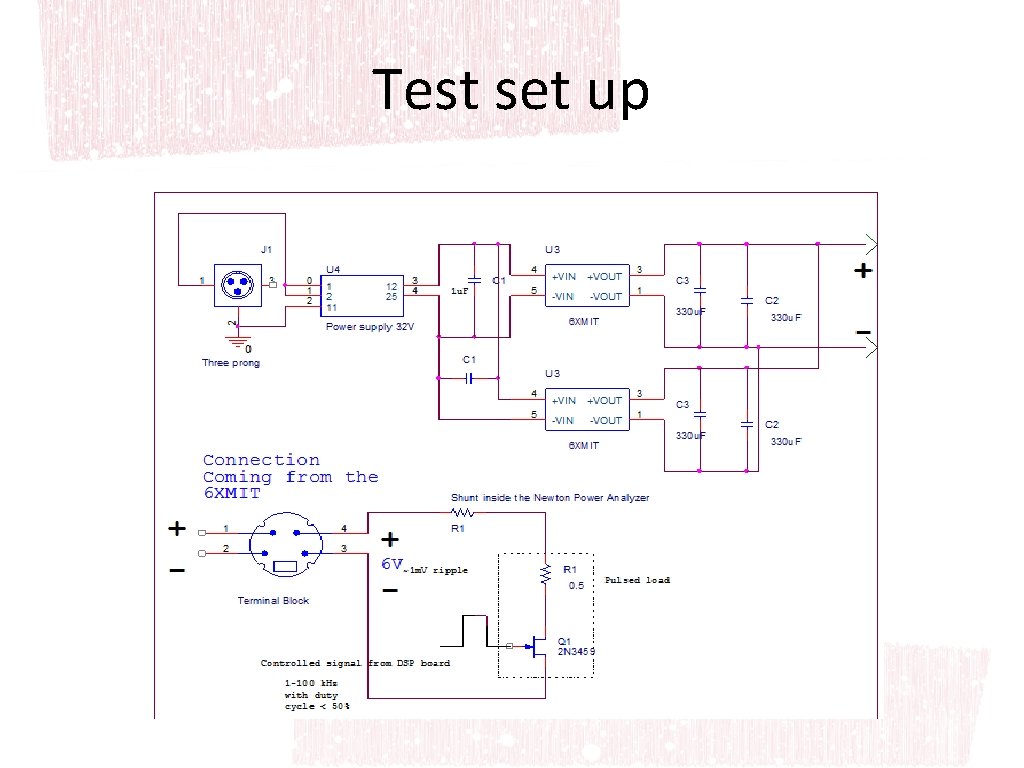
Test set up

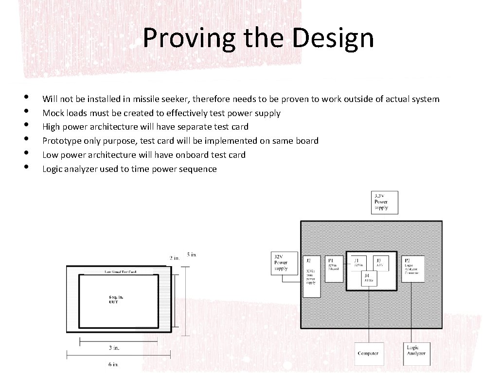
Proving the Design • • • Will not be installed in missile seeker, therefore needs to be proven to work outside of actual system Mock loads must be created to effectively test power supply High power architecture will have separate test card Prototype only purpose, test card will be implemented on same board Low power architecture will have onboard test card Logic analyzer used to time power sequence