QUARTIC TDC Development at Univ of Alberta Jim

QUARTIC TDC Development at Univ. of Alberta Jim Pinfold, Shengli Liu, Bill Burris, John Scaapman University of Alberta, December 2, 2008

Features: 8 Channel TDC Board Prototype • Targeting at below 20 ps RMS resolution; (STAR TOF reported 24 ps, ALICE TOF reported 20 ps, Ref: 1, 2) • 8 differential LVPECL input channels ; • 1 HPTDC (v 1. 3) chip from CERN in Very High Resolution Mode; • Altera Cyclone 2 FPGA, Cypress USB chip for local debug; • Serial LVDS link to connect to the main RODs; • Both USB and the Serial LVDS link provide the timing and control signals to HPTDC; Ref 1: J. Schambach, “Proposed STAR time of flight readout electronics and DAQ”, Computing in High Energy and Nuclear Physics, 2428, March 2003, La Jolla, California. Ref 2: P. Antonioli, “A 20 ps TDC readout module for the ALICE time of flight system: design and test results”. 9 th Workshop on Electronics for LHC Experiments, Amsterdam, The Netherlands, 29 Sep - 3 Oct 2003, pp. 311 -315

Development history: 8 Channel TDC Board Prototype • January to April 2008: Development of Schematics and PCB, FPGA coding/Simulation; • May: PCB assembly; • May to June: FPGA coding, TDC Programming and DLL, RC Parameter adjusting; • June to August: Performance testing at University of Alberta.

8 Channel TDC Board Prototype

2 boards and NIM-PECL, TTL-PECL translators

Testing setup Code Density Test for DNL, INL: Pulse Generator To PECL Quartic TDC Cable Delay Test for RMS resolution: Pulse Generator Pulse splitter To PECL Extra Cable Delay Quartic TDC To PECL Differential Nonlinearity Integral Nonlinearity

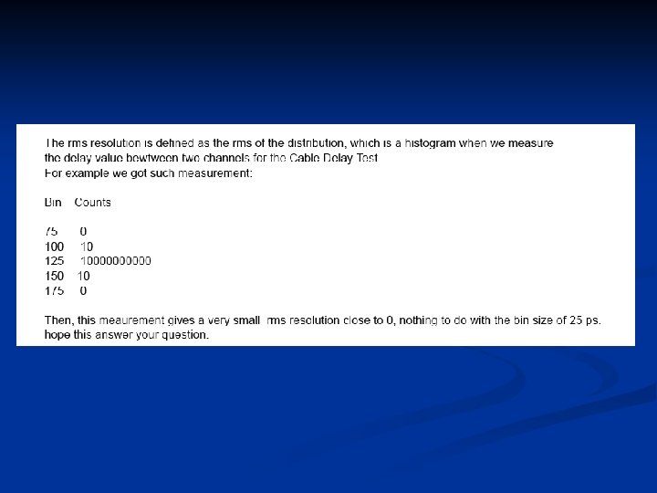
TDC’s RMS resolution The delay value between two signals plotted as histogram; RMS resolution = RMS of the delay value distribution; Single Channel RMS resolution = RMS resolution / sqrt(2);

HPTDC: DLL and R-C delay line Courtesy from J. Christiansen, “HPTDC Manual”

HPTDC: data bits combination Courtesy from J. Christiansen, “HPTDC Manual”

Testing results: DNL

Testing results: INL

Testing results: Summary for DNL and INL q All channels have the similar DNL patterns, values. q INL has very small changes on different channels. But still different INL compensation on each channel makes difference on resolution results. q 4 bit is enough for standard INL compensation. Standard means without expanding data bit width.

Testing results: RMS resolution without INL correction

Testing results: RMS resolution with INL correction

Testing results: RMS resolution with INL correction

Testing results: RMS resolution vs. delay

Testing results: RMS resolution for channel 0 to other channels

Summary ü 2 TDC boards have been built and tested, each with 8 input VHRM (Very High Resolution Mode: 25 ps bin size) with USB interface and LVDS link to downstream Read out. ü RMS resolution is smaller than 15 ps for both boards with 4 bit INL compensation. ü RMS resolution is smaller than 12 ps for both boards with 8 bit INL compensation. ü RMS resolution performance does not change very much among different channels, and not very much either for different delay time in the range of 25 ns. (periodically with 25 ns)

- Slides: 20