Quarterly Technical Report 1 for Pittsburgh Digital Greenhouse
Quarterly Technical Report 1 for Pittsburgh Digital Greenhouse High Speed CMOS A/D Converter Circuit for Radio Frequency Signal Kyusun Choi Computer Science and Engineering Department The Pennsylvania State University 1
Project goals for this quater 1. Design a 6 and 8 bit TIQ based flash ADC circuits and CMOS layouts 2. Design the first prototype chip: 6 and 8 bit flash ADC 3. Chip fabrication submission 2
Accomplished project milestones for this quarter 1. Designed 6, 8, and 9 bit TIQ based ADC circuits and CMOS layouts in 0. 25 m 2. Designed the first prototype chip: 6, 8, and 9 bit flash ADC 3. Fabrication submission preparation 4. Chip fabrication submission: - Submission date: 4/2/2001 - Vendor: MOSIS with TSMC 0. 25 m foundry - Expected prototype chip delivery date: 7/16/2001 3
Design Method 1. Systematic Variation Approach - Systematic Parameter Variation (SPV) 2. CAD Tools - MAX for layout - SUE for schematic capture - HSPICE for circuit simulation - Custom designed a set of C programs 3. Experiment base, Spice Model Base 4
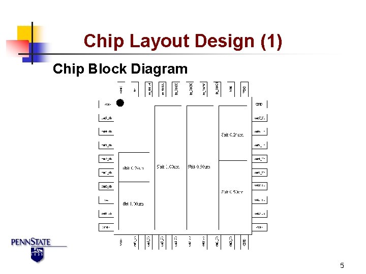
Chip Layout Design (1) Chip Block Diagram 5
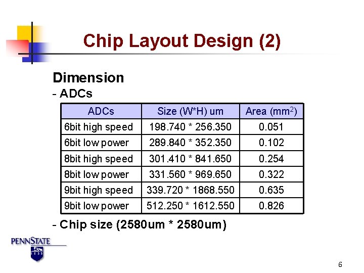
Chip Layout Design (2) Dimension - ADCs Size (W*H) um Area (mm 2) 6 bit high speed 198. 740 * 256. 350 0. 051 6 bit low power 289. 840 * 352. 350 0. 102 8 bit high speed 301. 410 * 841. 650 0. 254 8 bit low power 331. 560 * 969. 650 0. 322 9 bit high speed 339. 720 * 1868. 550 0. 635 9 bit low power 512. 250 * 1612. 550 0. 826 - Chip size (2580 um * 2580 um) 6
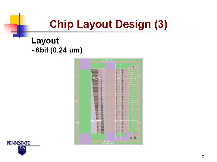
Chip Layout Design (3) Layout - 6 bit (0. 24 um) 7
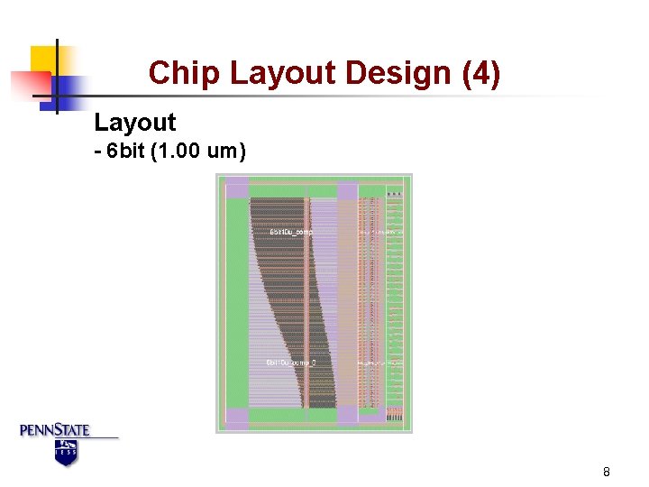
Chip Layout Design (4) Layout - 6 bit (1. 00 um) 8
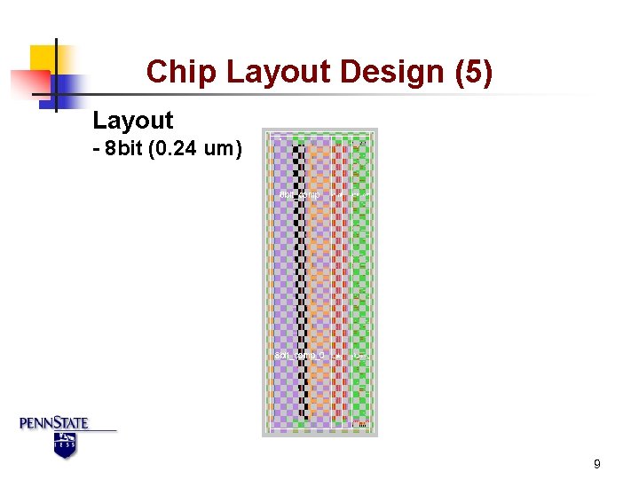
Chip Layout Design (5) Layout - 8 bit (0. 24 um) 9
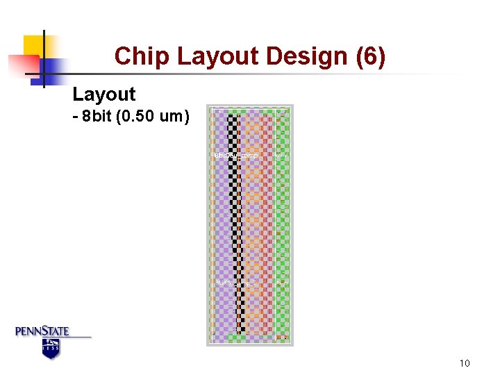
Chip Layout Design (6) Layout - 8 bit (0. 50 um) 10
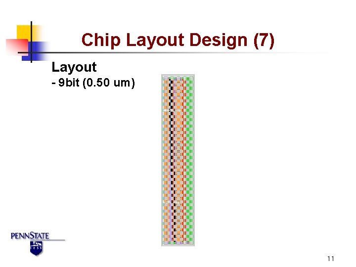
Chip Layout Design (7) Layout - 9 bit (0. 50 um) 11
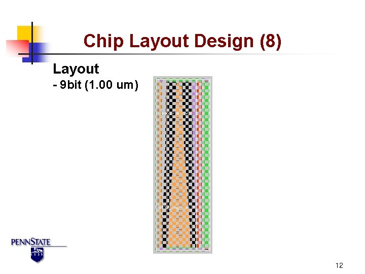
Chip Layout Design (8) Layout - 9 bit (1. 00 um) 12
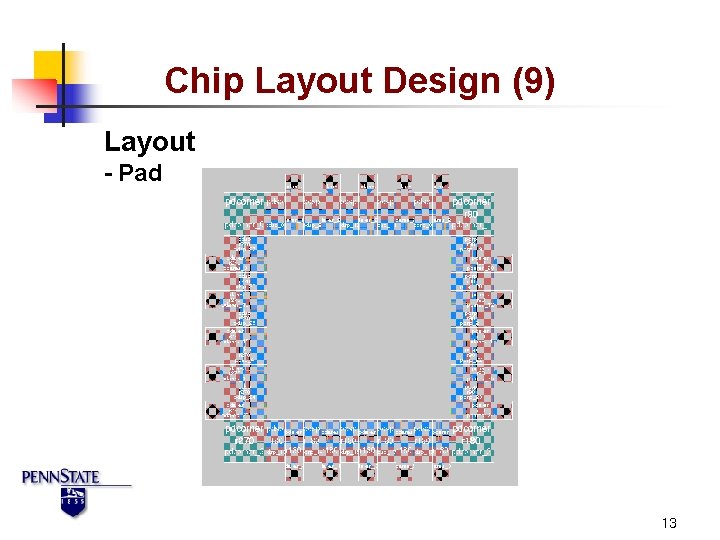
Chip Layout Design (9) Layout - Pad 13
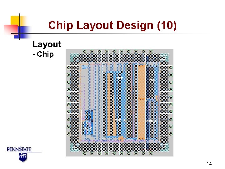
Chip Layout Design (10) Layout - Chip 14
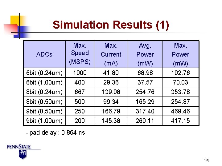
Simulation Results (1) ADCs Max. Speed (MSPS) Max. Current (m. A) Avg. Power (m. W) Max. Power (m. W) 6 bit (0. 24 um) 1000 41. 80 68. 98 102. 76 6 bit (1. 00 um) 400 29. 36 37. 57 70. 03 8 bit (0. 24 um) 667 139. 08 254. 76 353. 78 8 bit (0. 50 um) 500 99. 34 165. 29 254. 87 9 bit (0. 50 um) 250 166. 79 317. 40 469. 46 9 bit (1. 00 um) 200 145. 38 260. 11 417. 15 - pad delay : 0. 864 ns 15
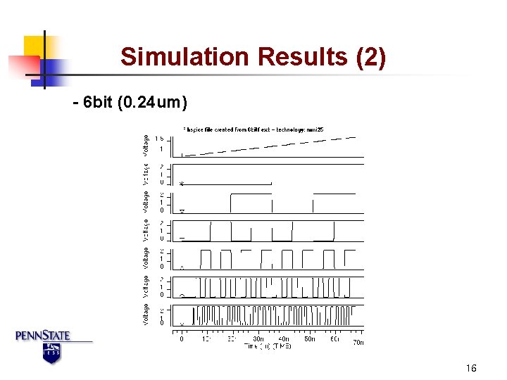
Simulation Results (2) - 6 bit (0. 24 um) 16
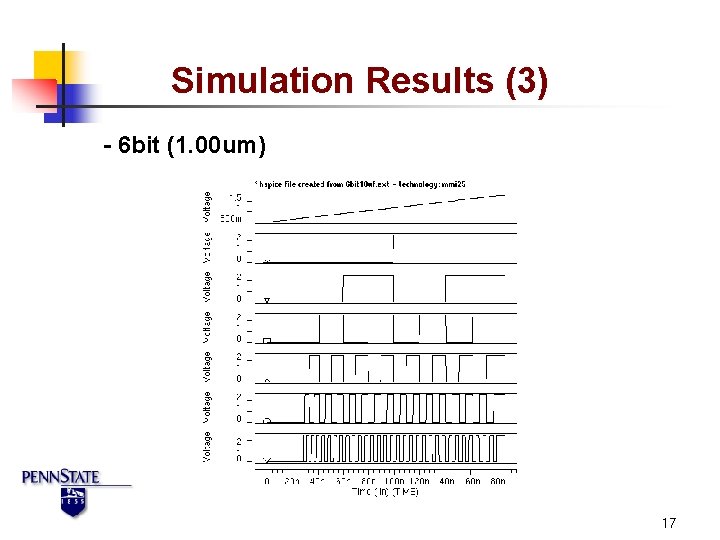
Simulation Results (3) - 6 bit (1. 00 um) 17
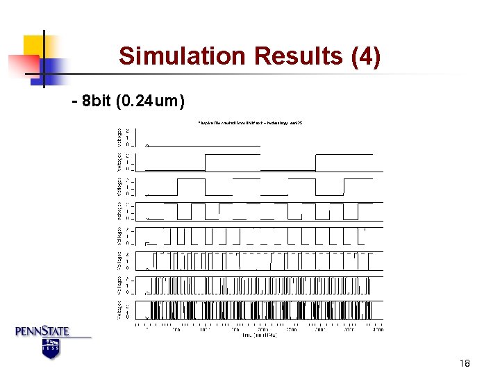
Simulation Results (4) - 8 bit (0. 24 um) 18
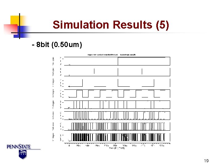
Simulation Results (5) - 8 bit (0. 50 um) 19
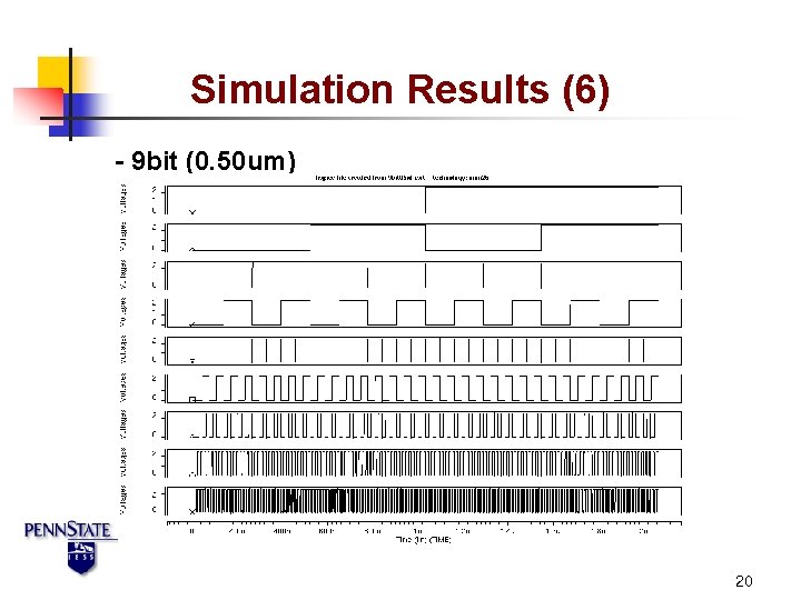
Simulation Results (6) - 9 bit (0. 50 um) 20
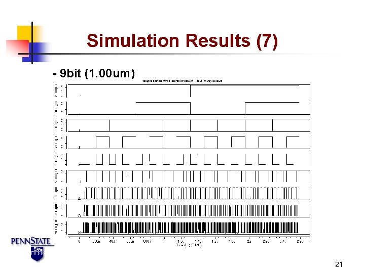
Simulation Results (7) - 9 bit (1. 00 um) 21
Features of the TIQ based ADC 1. High Speed 2. Relatively small area 3. Relatively low-power 22
Issues to Be Addressed in Future 1. Dynamic fine-tuning 2. Supply voltage variation compensation 3. Temperature variation compensation 4. Process variation compensation 5. Lower power 6. FIFO design for on-chip high-speed data acquisition 23
Innovation Challenges • • • 2 GSPS with 0. 18 um CMOS Custom layout CAD tool 10 bit and 12 bit ADC Low power Dynamic calibration • • • Offset Gain Temperature Power supply voltage Process parameter variation 24
Summary • High speed ADC for RF • ADC core - 6, 8 and 9 bit design • first prototype chip (silicon test) • 0. 25 m MOSIS (tsmc) process • CMOS digital logic technology • Future ready • Dynamic calibration 25
- Slides: 25