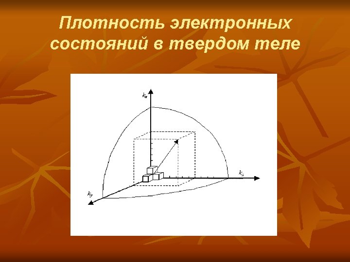
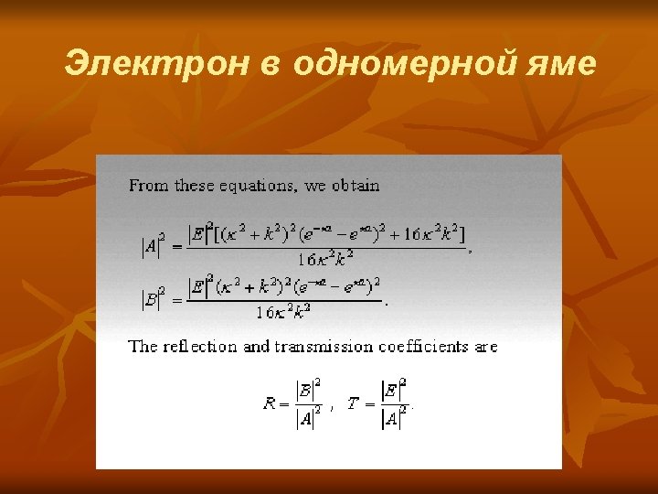
Quantum Wells Quantum Well Enclosed region of negative


 n n n Substrate wafers transferred to high vacuum growth")
")


- Slides: 54
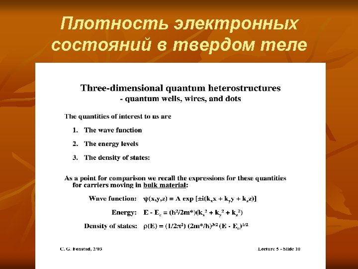
Quantum Wells Quantum Well • Enclosed region of negative energy • Electrons confined • Can exist in one, two, three dimensions • Common example is a square well – sharpest boundary • Discrete energies of electrons • Narrow gap semiconductor between wide gap semiconductors • Surfaces states may be considered like quantum well states 10 cm - e moves freely e confined 10 cm 10 nm thick Nanoscale Thin Film Quantum Well
Quantum Well Applications Multi-spectral long wavelength quantum well infrared photodetectors: infrared radiation photoionize trapped carriers in quantum wells; for medical applications, locating hot spots in fires, observing volcanoes Quantum well lasers: quantum confinement effects increase luminescence efficiency Quantum well LEDs Quantum well Hall (magnetic) sensors JPL’s QWIP detects minute differences associated with blood flow changes Quantum well laser mounted on the head of a pin: http: //wwwrsphysse. anu. edu. au/admin/pgbrochure/quantum. html http: //www. jpl. nasa. gov/technology/shrinking/tiny_tech. html
n Superlattices Alternating layers of thin films additional periodicity causes interesting effects n When l , λ > b → phonon wave and particle effects n Electron transport well understood n Limited understanding of phonon transport Are layers thin enough for electrons/phonons to tunnel? Is coherence maintained for mini-band formation? b Si 0. 76 Ge 0. 24 / Si 0. 84 Ge 0. 16 superlattice: Electron tunneling In a crystal, atomic periodicity leads to band formation In a superlattice, engineered periodicity leads to minibands
Superlattice Applications Magnetic superlattices for magneto-optical recording: large perpendicular anisotropies and enhancement of Kerr rotations provide unique properties Giant magnetoresistance Superlattice field effect transistors Thermoelectric materials Commercially available superlattice thermoelectric device from RTI http: //www. nuee. nagova-u. ac. jp/labs http: //www. rti. org/pubs/anser. pdf Superlattice used in thermoelectrics: Metallic superlattice for GMR
Semiconductor Band Gaps n n n Energy states in an atom correspond to bands in a semiconductor In between the valence and conduction bands, there are no states where an electron can exist Electron-hole pairs (EHPs) can form by thermal or photo excitation Electrons in the conduction band are free to conduct electricity Different semiconductors have different band gaps EC EG EV
The Energy Levels of Quantum Dots The Quantum Dot band gap is smaller than the n n E surrounding material, so electrons will tend to “fall” into the dot to reach a lower-energy configuration Because the Quantum Dots are so small (20 -30 nm), quantum mechanics govern how an electron will behave in the dot electron EC EG e- EV hole
The Quantum Dot n n Confinement in all three dimensions Ex, Ey, and Ez are quantized (discrete) Higher probability of recombination means greater radiative emission “Electronic Structure of In. As Pyramidal Quantum Dots”: http: //www. sst. nrel. gov/research/In. As. html Ee = Ez + Ex + Ey with all E discrete
Molecular Beam Epitaxy (MBE) n n n Substrate wafers transferred to high vacuum growth chamber (red arrow) Elements kept in K-Cells at high temp Shutters over cells open to release vaporized elements, which deposit on sample Adapted from: Farrow, R. F. C. , ed. Molecular Beam Epitaxy: Applications to Key Materials. Noyes Publications, Park Ridge, NJ, 1995.
Molecular Beam Epitaxy (MBE)
More About MBE n n The temperature of each K-Cell controls the rate of deposition of that element (Ga, In, Al, etc. ) As and P can also be flowed into chamber Precise control over temperatures and shutters allows very thin layers to be grown (~1 ML/sec) RHEED patterns indicate surface morphology
Fabrication of Wells n n n Lattice matched Al. Ga. As grown on Ga. As substrate Thin layer of Ga. As (~10 nm) Another layer of Al. Ga. As to finish the well d 2 d 1 = d 2 z
Fabrication of Dots n n Thick layer of Ga. As Begin growing In. As (greater lattice constant) Crystal strain forces dot formation Cap dots with layer of Ga. As d 1 d 2 d 1 z
Epitaxy: Patterned Growth n Growth on patterned substrates n n n Grow QDs in pyramidshaped recesses Recesses formed by selective ion etching Disadvantage: density of QDs limited by mask pattern T. Fukui et al. Ga. As tetrahedral quantum dot structures fabricated using selective area metal organic chemical vapor deposition. Appl. Phys. Lett. May, 1991
Epitaxy: Self-Organized Growth n Self-organized QDs through epitaxial growth strains n Stranski-Krastanov growth mode (use MBE, MOCVD) n n n Islands formed on wetting layer due to lattice mismatch (size ~10 s nm) Disadvantage: size and shape fluctuations, ordering Control island initiation n imagesconditions, of islands Induce local strain, grow on dislocation, vary AFM growth epitaxiall grown on Ga. As combine with patterning substrate. (a) In. As islands randomly nucleate. (b) Random distribution of Inx. Ga 1 x. As ring shaped islands. (c) A 2 D lattice of In. As islands on a Ga. As substrate. P. Petroff, A. Lorke, and A. Imamoglu. Epitaxially self-assembled quantum dots. Physics Today, May 2001.
QCA: Physics Basics Cell Quantum Dot Empty Containing electron - Tunnel – allows electrons to move between dots Using cells w/2 electrons. ? Possible configurations? - ? “ 0” - “ 1” Only 2, since electrons repel each other. “Low energy state”
QCA: Physics Basics Adjacent cells’ electrons also repel each other. - - - or - Consumes/generates no energy. -
QCA: Wires - - - - Adjacent cells in low-energy state One cell “fixed” to some value. - Electrons move into low-energy state. Value propogates. - - - -
QCA: Wires - Same when rotated to vertical.
QCA: Wires - - - Same idea when cells rotated 45º. - Note complementation! - - -
QCA: Wire Crossings - - - - - Such wires cross w/o interference. -
QCA: Wire Crossings - - Same value - - -
QCA: Gates Fixed inputs ? - Output - - What function computed? ? Majority. I. e. , most common input value. a b c maj. 0 0 0 1 1 0 0 0 1 1 1 1 0 1
Clocked Molecular Quantum-dot Cellular Automata Molecular quantum-dot proposed by Lent – Isakcsen n Allyl Alkyl
Clocked Molecular Quantum-dot Cellular Automata n n Allyl groups serve as dots with his red-ox centre that can be achieved cy halls Alkyl groups serve as tunnel barrier that halls can pass through