Quality Assurance for the ATLAS Pixel Sensor 1

- Slides: 23

Quality Assurance for the ATLAS Pixel Sensor 1 st Workshop on Quality Assurance Issues in Silicon Detectors J. M. Klaiber-Lodewigs (Univ. Dortmund) for the ATLAS pixel collaboration Contents: - role of the pixel sensor - overall QA concept - measurement of bulk parameters - sensor breakdown - sensor depletion - time stability - radiation hardness - cross calibration 1 st Workshop on QA Issues in Si Detectors, May 2001, Genève QA for the ATLAS Pixel Sensor,

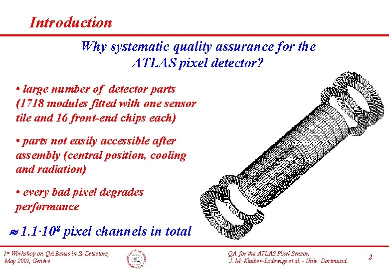
Introduction Why systematic quality assurance for the ATLAS pixel detector? • large number of detector parts (1718 modules fitted with one sensor tile and 16 front-end chips each) • parts not easily accessible after assembly (central position, cooling and radiation) • every bad pixel degrades performance 1. 1· 108 pixel channels in total 1 st Workshop on QA Issues in Si Detectors, May 2001, Genève QA for the ATLAS Pixel Sensor, J. M. Klaiber-Lodewigs et al. - Univ. Dortmund 2

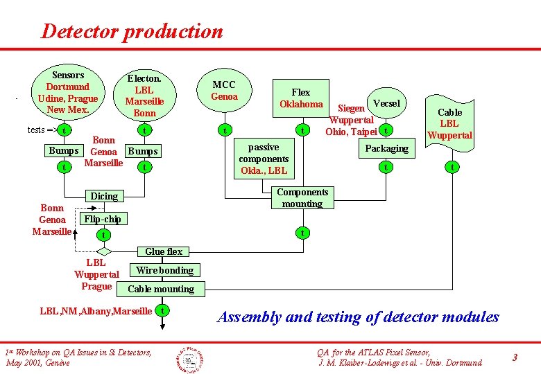
Detector production Sensors Dortmund Udine, Prague New Mex. Electon. LBL Marseille Bonn tests => t t Bonn Bumps Genoa Bumps Marseille t t Flex Oklahoma t t Vecsel Siegen Wuppertal Ohio, Taipei t passive components Okla. , LBL Cable LBL Wuppertal Packaging t t Components mounting Dicing Bonn Genoa Marseille MCC Genoa Flip-chip t t Glue flex LBL Wire bonding Wuppertal Prague Cable mounting LBL, NM, Albany, Marseille t 1 st Workshop on QA Issues in Si Detectors, May 2001, Genève Assembly and testing of detector modules QA for the ATLAS Pixel Sensor, J. M. Klaiber-Lodewigs et al. - Univ. Dortmund 3

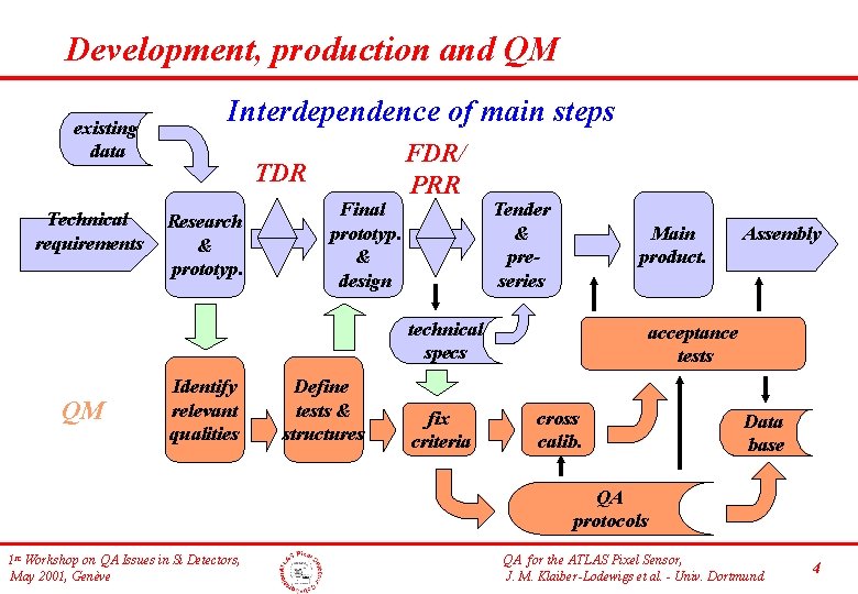
Development, production and QM existing data Technical requirements Interdependence of main steps TDR Research & prototyp. Final prototyp. & design FDR/ PRR Tender & preseries Main product. technical specs QM Identify relevant qualities Define tests & structures fix criteria Assembly acceptance tests cross calib. Data base QA protocols 1 st Workshop on QA Issues in Si Detectors, May 2001, Genève QA for the ATLAS Pixel Sensor, J. M. Klaiber-Lodewigs et al. - Univ. Dortmund 4

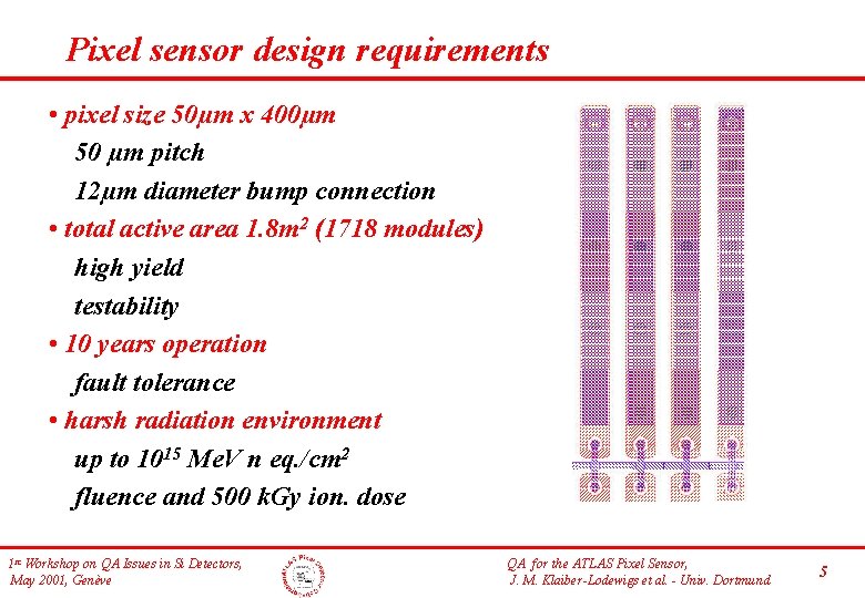
Pixel sensor design requirements • pixel size 50µm x 400µm 50 µm pitch 12µm diameter bump connection • total active area 1. 8 m 2 (1718 modules) high yield testability • 10 years operation fault tolerance • harsh radiation environment up to 1015 Me. V n eq. /cm 2 fluence and 500 k. Gy ion. dose 1 st Workshop on QA Issues in Si Detectors, May 2001, Genève QA for the ATLAS Pixel Sensor, J. M. Klaiber-Lodewigs et al. - Univ. Dortmund 5

Development Strategy Design studies Studies on silicon - performed within ATLAS - performed within ROSE - prototype sensors - various Si impurities concerning - isolation technique - design of the pixel cell concerning - damage parameters - fabrication process Radiation tolerant sensors 1 st Workshop on QA Issues in Si Detectors, May 2001, Genève QA for the ATLAS Pixel Sensor, J. M. Klaiber-Lodewigs et al. - Univ. Dortmund 6

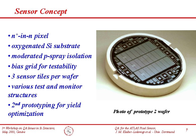
Sensor Concept • n+-in-n pixel • oxygenated Si substrate • moderated p-spray isolation • bias grid for testability • 3 sensor tiles per wafer • various test and monitor structures • 2 nd prototyping for yield optimization 1 st Workshop on QA Issues in Si Detectors, May 2001, Genève Photo of prototype 2 wafer QA for the ATLAS Pixel Sensor, J. M. Klaiber-Lodewigs et al. - Univ. Dortmund 7

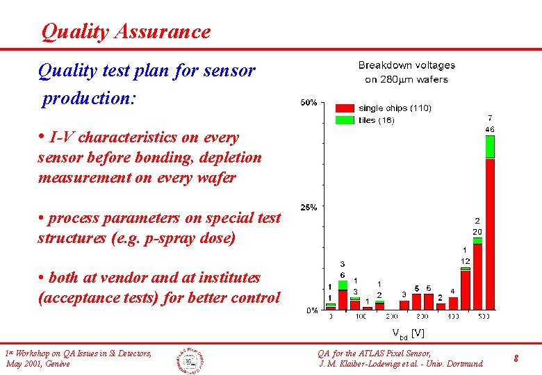
Quality Assurance Quality test plan for sensor production: • I-V characteristics on every sensor before bonding, depletion measurement on every wafer • process parameters on special test structures (e. g. p-spray dose) • both at vendor and at institutes (acceptance tests) for better control 1 st Workshop on QA Issues in Si Detectors, May 2001, Genève QA for the ATLAS Pixel Sensor, J. M. Klaiber-Lodewigs et al. - Univ. Dortmund 8

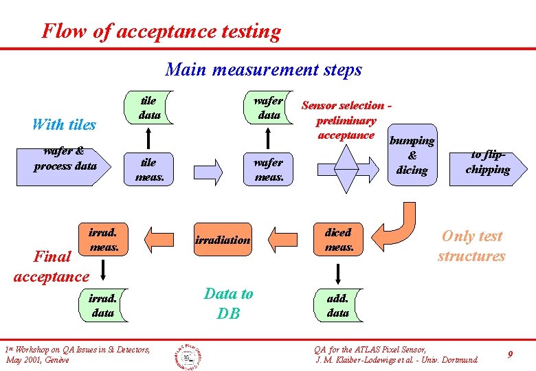
Flow of acceptance testing Main measurement steps With tiles wafer & process data tile data wafer data tile meas. wafer meas. irradiation irrad. data Data to DB Final acceptance 1 st Workshop on QA Issues in Si Detectors, May 2001, Genève Sensor selection preliminary acceptance bumping & dicing diced meas. to flipchipping Only test structures add. data QA for the ATLAS Pixel Sensor, J. M. Klaiber-Lodewigs et al. - Univ. Dortmund 9

Tests to perform Grouped in topical order 1 st Workshop on QA Issues in Si Detectors, May 2001, Genève QA for the ATLAS Pixel Sensor, J. M. Klaiber-Lodewigs et al. - Univ. Dortmund 10

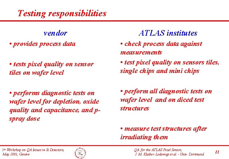
Testing responsibilities vendor • provides process data • tests pixel quality on sensor tiles on wafer level • performs diagnostic tests on wafer level for depletion, oxide quality and capacitance, and pspray dose ATLAS institutes • check process data against measurements • test pixel quality on sensors tiles, single chips and mini chips • perform all diagnostic tests on wafer level and on diced test structures • measure test structures after irradiating them 1 st Workshop on QA Issues in Si Detectors, May 2001, Genève QA for the ATLAS Pixel Sensor, J. M. Klaiber-Lodewigs et al. - Univ. Dortmund 11

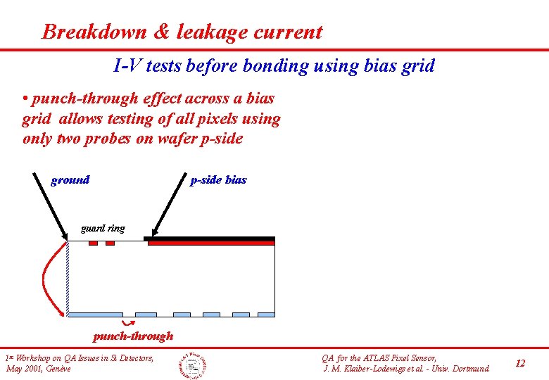
Breakdown & leakage current I-V tests before bonding using bias grid • punch-through effect across a bias grid allows testing of all pixels using only two probes on wafer p-side ground p-side bias guard ring punch-through 1 st Workshop on QA Issues in Si Detectors, May 2001, Genève QA for the ATLAS Pixel Sensor, J. M. Klaiber-Lodewigs et al. - Univ. Dortmund 12

Testability of pixel quality I-V tests on test pixels using punch-through current through single pixel current through punch-through array Leakage current indicative for quality of every pixel 1 st Workshop on QA Issues in Si Detectors, May 2001, Genève QA for the ATLAS Pixel Sensor, J. M. Klaiber-Lodewigs et al. - Univ. Dortmund 13

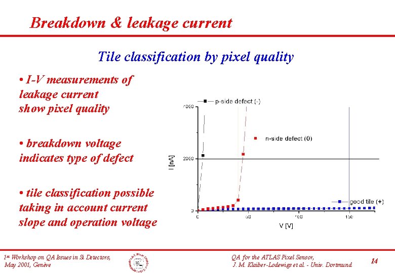
Breakdown & leakage current Tile classification by pixel quality • I-V measurements of leakage current show pixel quality • breakdown voltage indicates type of defect • tile classification possible taking in account current slope and operation voltage 1 st Workshop on QA Issues in Si Detectors, May 2001, Genève QA for the ATLAS Pixel Sensor, J. M. Klaiber-Lodewigs et al. - Univ. Dortmund 14

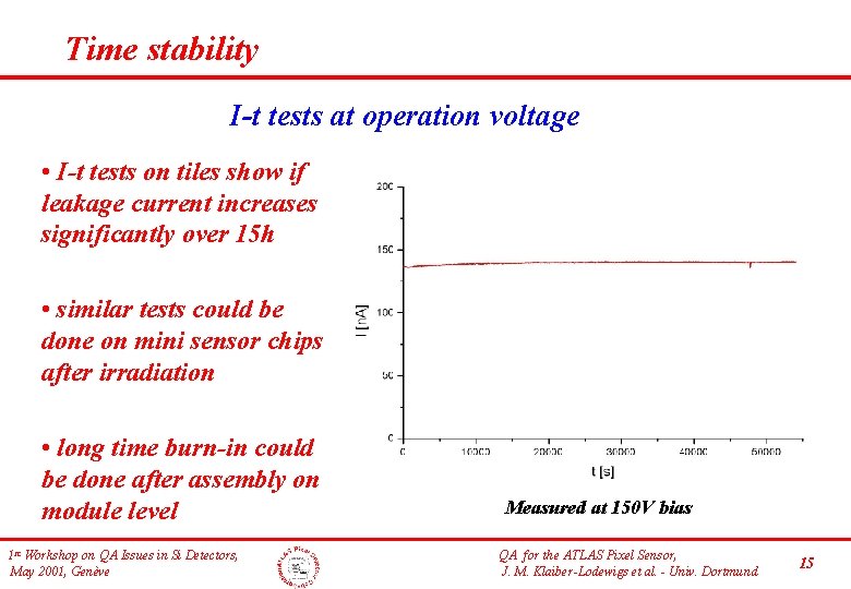
Time stability I-t tests at operation voltage • I-t tests on tiles show if leakage current increases significantly over 15 h • similar tests could be done on mini sensor chips after irradiation • long time burn-in could be done after assembly on module level 1 st Workshop on QA Issues in Si Detectors, May 2001, Genève Measured at 150 V bias QA for the ATLAS Pixel Sensor, J. M. Klaiber-Lodewigs et al. - Univ. Dortmund 15

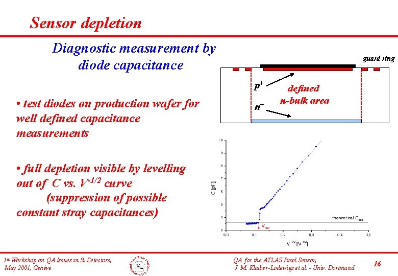
Sensor depletion Diagnostic measurement by diode capacitance guard ring p+ • test diodes on production wafer for well defined capacitance measurements n+ defined n-bulk area • full depletion visible by levelling out of C vs. V-1/2 curve (suppression of possible constant stray capacitances) 1 st Workshop on QA Issues in Si Detectors, May 2001, Genève QA for the ATLAS Pixel Sensor, J. M. Klaiber-Lodewigs et al. - Univ. Dortmund 16

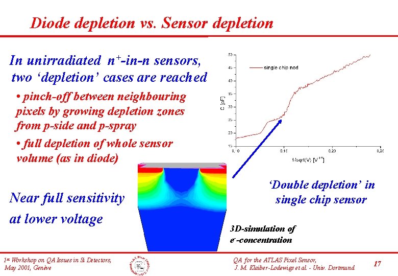
Diode depletion vs. Sensor depletion In unirradiated n+-in-n sensors, two ‘depletion’ cases are reached • pinch-off between neighbouring pixels by growing depletion zones from p-side and p-spray • full depletion of whole sensor volume (as in diode) Near full sensitivity at lower voltage 1 st Workshop on QA Issues in Si Detectors, May 2001, Genève ‘Double depletion’ in single chip sensor 3 D-simulation of e--concentration QA for the ATLAS Pixel Sensor, J. M. Klaiber-Lodewigs et al. - Univ. Dortmund 17

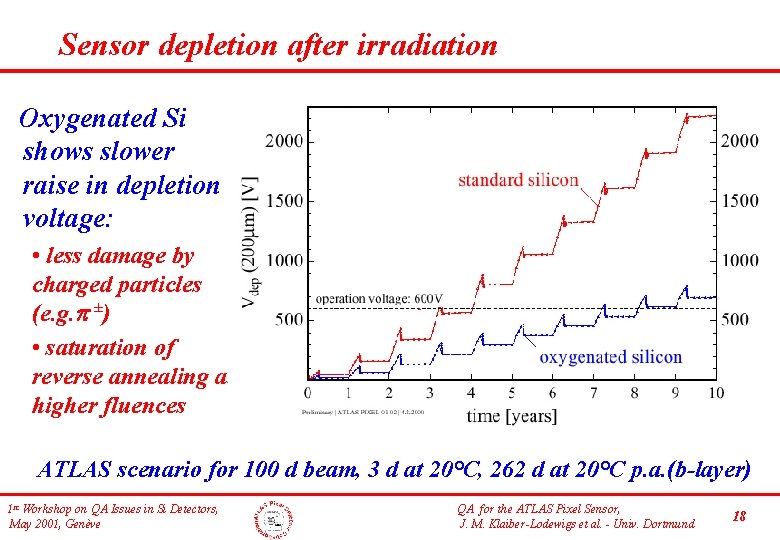
Sensor depletion after irradiation Oxygenated Si shows slower raise in depletion voltage: • less damage by charged particles (e. g. ±) • saturation of reverse annealing at higher fluences ATLAS scenario for 100 d beam, 3 d at 20°C, 262 d at 20°C p. a. (b-layer) 1 st Workshop on QA Issues in Si Detectors, May 2001, Genève QA for the ATLAS Pixel Sensor, J. M. Klaiber-Lodewigs et al. - Univ. Dortmund 18

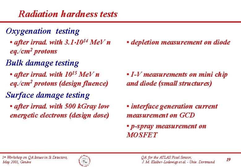
Radiation hardness tests Oxygenation testing • after irrad. with 3. 1 1014 Me. V n eq. /cm 2 protons • depletion measurement on diode Bulk damage testing • after irrad. with 1015 Me. V n eq. /cm 2 protons (design fluence) • I-V measurements on mini chip and diode (small structures) Surface damage testing • after irrad. with 500 k. Gray low energetic electrons (design dose) 1 st Workshop on QA Issues in Si Detectors, May 2001, Genève • interface generation current measurement on GCD • p-spray measurement on MOSFET QA for the ATLAS Pixel Sensor, J. M. Klaiber-Lodewigs et al. - Univ. Dortmund 19

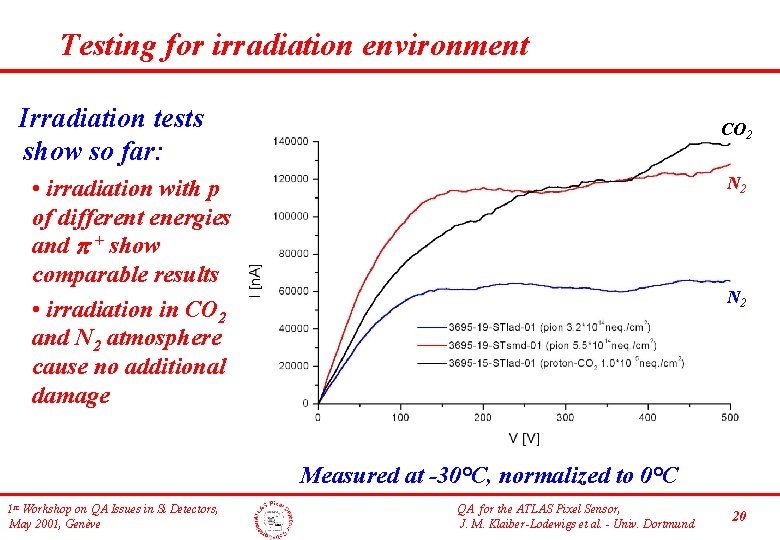
Testing for irradiation environment Irradiation tests show so far: CO 2 N 2 • irradiation with p of different energies and + show comparable results • irradiation in CO 2 and N 2 atmosphere cause no additional damage N 2 Measured at -30°C, normalized to 0°C 1 st Workshop on QA Issues in Si Detectors, May 2001, Genève QA for the ATLAS Pixel Sensor, J. M. Klaiber-Lodewigs et al. - Univ. Dortmund 20

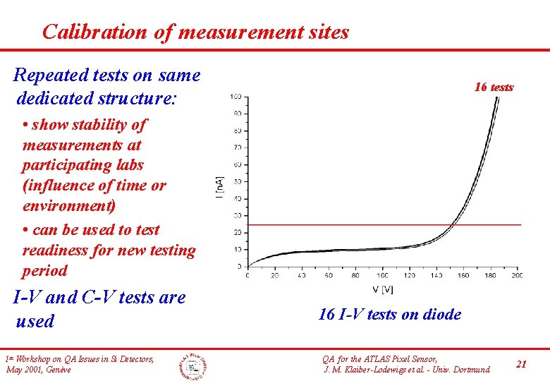
Calibration of measurement sites Repeated tests on same dedicated structure: 16 tests • show stability of measurements at participating labs (influence of time or environment) • can be used to test readiness for new testing period I-V and C-V tests are used 1 st Workshop on QA Issues in Si Detectors, May 2001, Genève 16 I-V tests on diode QA for the ATLAS Pixel Sensor, J. M. Klaiber-Lodewigs et al. - Univ. Dortmund 21

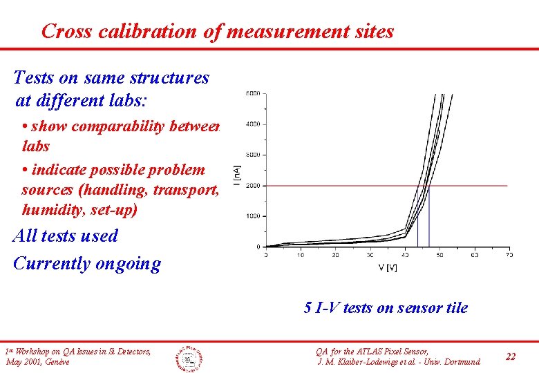
Cross calibration of measurement sites Tests on same structures at different labs: • show comparability between labs • indicate possible problem sources (handling, transport, humidity, set-up) All tests used Currently ongoing 5 I-V tests on sensor tile 1 st Workshop on QA Issues in Si Detectors, May 2001, Genève QA for the ATLAS Pixel Sensor, J. M. Klaiber-Lodewigs et al. - Univ. Dortmund 22

Summary QM for the ATLAS pixel sensor • has been a dynamic process between different aspects of the project • requires close collaboration for a long time period QA procedures have required • good understanding of the phenomena to be measured • decisions on what exactly is crucial or worthwhile to know QC measurements have, until now • given us good tools for acceptance decisions • ensured compatibility between different measurements / scenario and test 1 st Workshop on QA Issues in Si Detectors, May 2001, Genève QA for the ATLAS Pixel Sensor, J. M. Klaiber-Lodewigs et al. - Univ. Dortmund 23