QPSK Quadrature Phase Shift Keying Quadrature Phase Shift

 is a form of")


 • The Johnson counter (÷ by 4) can be")

 • CD 4027 BMS is a single monolithic chip")


 • The LM 324 series has quad op-amps with")

")
")


 • The CD 4052 analog multiplexers demultiplexers are digitally")


- Slides: 28
QPSK
Quadrature Phase Shift Keying • Quadrature Phase Shift Keying (QPSK) is a form of Phase Shift Keying in which two bits are taken at a time and modulated, selecting one of four possible carrier phase shifts (0, 90, 180, or 270 degrees). • QPSK allows the signal to carry twice much information than ordinary PSK, using the same bandwidth.
QPSK Waveforms
QPSK APPLICATIONS • • • Satellite transmission of MPEG 2 video cable modems Videoconferencing cellular phone systems other forms of digital communication over an RF carrier
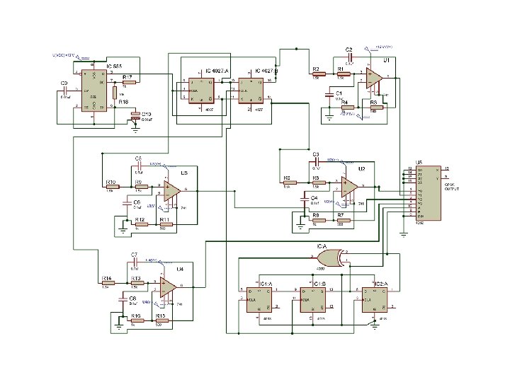
HARDWARE IMPLEMENTATION • Design a 555 clock generator at a frequency of 12 k. Hz. Construct a divide by 4 Johnson counter using JK flip flops to generate four phases of square waves. • The four phases are given to four second order LPFs to obtain two sine waves (+sine, -sine) and two cosine waves (+cosine, -cosine). • Finally, those four signals are given to the 4: 1 multiplexer (4052).
HARDWARE IMPLEMENTATION • Design a 3 -bit PRBS generator using 4013 -D Flip Flops. • The clock for this data generator is from Q 1 of Johnson counter as shown in the block diagram. (NEXT SLIDE) • The select lines of 4052 are connected to the PRBS generator. • The 4052 output is the desired QPSK signal.
BLOCK DIAGRAM
DATA INPUTS SELECTING CARRIER
CLOCK FROM IC 555
FREQUENCY CALCULATION • The clock signal can be generated by IC 555, operating in the Astable mode. The frequency of that clock signal can be calculated by • f= 1/t • t=0. 69 RC • t=0. 69 (10 k) (0. 01 uf) • f=14. 492 k. Hz
JOHNSON COUNTER (DIVIDE BY FOUR) • The Johnson counter (÷ by 4) can be designed using JK Flip Flop as shown in figure to generate the four phases of square waves.
OUTPUT WAVEFORM
CMOS JK FLIP FLOP (4027) • CD 4027 BMS is a single monolithic chip integrated circuit containing two identical complementary-symmetry J-K master slave flip-flops. • Each flip-flop has provisions for individual J, K, Set Reset, and Clock input signals. • Buffered Q and Q signals are available as outputs. • The CD 4027 BMS is supplied in these 16 -lead outline packages
PINOUT OF 4027
SECOND ORDER LOW PASS FILTER • The second order Low pass filter can be constructed using op-amp as shown in figure, to convert the square wave into sine waveform. • We need to convert the square wave of four different phases, so, we can use LM 324 (Quad op-amp), which consists of four op-amps within a single DIP chip.
SECOND ORDER LPF USING OPAMP
QUAD OP AMP (LM 324) • The LM 324 series has quad op-amps with true differential inputs. • The quad amplifier can operate at supply voltages as low as 3. 0 V or as high as 32 V. FEATURES • Short Circuited Protected Outputs • True Differential Input Stage • Single Supply Operation: 3. 0 V to 32 V (LM 224, LM 324 A) or + 16 V • Four Amplifiers Per Package
PINOUT OF LM 324
OUTPUT WAVEFORM OF LM 324 (PIN NUMBER 1 AND 7)
OUTPUT WAVEFORM OF LM 324 (PIN NUMBER 8 AND 14)
OUTPUT WAVEFORMS
PRBS DATA GENERATOR
OUTPUT WAVEFORM OF CLOCK AND PRBS
CMOS 4: 1 MULTIPLEXER (4052) • The CD 4052 analog multiplexers demultiplexers are digitally controlled analog switches. • Control of analog signals up to 15 Vp-p can be achieved by digital signal amplitudes of 3− 15 V.
4052 PINOUT
MUX IMPLEMENTATION
QPSK OUTPUT