PXD Summary Agenda PXD Session July 23 2012
- Slides: 16

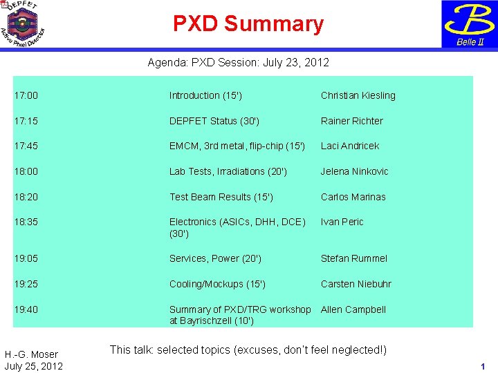
PXD Summary Agenda: PXD Session: July 23, 2012 17: 00 Introduction (15') Christian Kiesling 17: 15 DEPFET Status (30') Rainer Richter 17: 45 EMCM, 3 rd metal, flip-chip (15') Laci Andricek 18: 00 Lab Tests, Irradiations (20') Jelena Ninkovic 18: 20 Test Beam Results (15') Carlos Marinas 18: 35 Electronics (ASICs, DHH, DCE) (30') Ivan Peric 19: 05 Services, Power (20') Stefan Rummel 19: 25 Cooling/Mockups (15') Carsten Niebuhr 19: 40 Summary of PXD/TRG workshop Allen Campbell at Bayrischzell (10') H. -G. Moser July 25, 2012 This talk: selected topics (excuses, don’t feel neglected!) 1

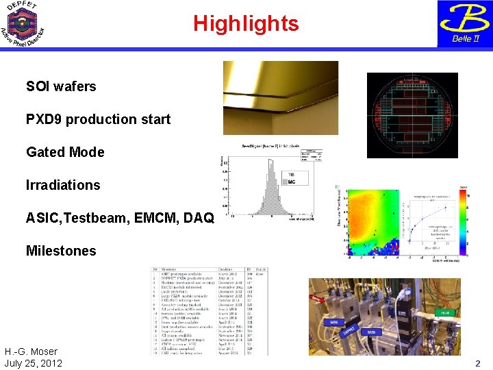
Highlights SOI wafers PXD 9 production start Gated Mode Irradiations ASIC, Testbeam, EMCM, DAQ Milestones H. -G. Moser July 25, 2012 2

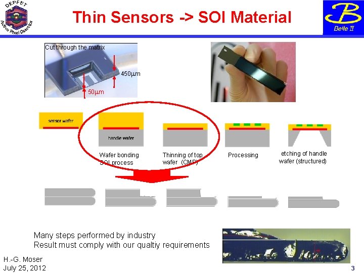
Thin Sensors -> SOI Material Cut through the matrix 450 mm Wafer bonding SOI process Thinning of top wafer (CMP) Processing etching of handle wafer (structured) Many steps performed by industry Result must comply with our qualtiy requirements H. -G. Moser July 25, 2012 3

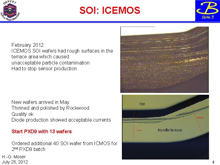
SOI: ICEMOS February 2012: ICEMOS SOI wafers had rough surfaces in the terrace area which caused unacceptable particle contamination Had to stop sensor production New wafers arrived in May Thinned and polished by Rockwood Quality ok Diode production showed acceptable currents Start PXD 9 with 13 wafers Ordered additional 40 SOI wafer from ICMOS for 2 nd PXD 9 batch H. -G. Moser July 25, 2012 4

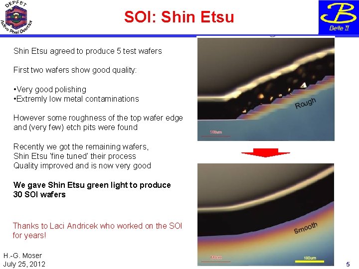
SOI: Shin Etsu agreed to produce 5 test wafers First two wafers show good quality: • Very good polishing • Extremly low metal contaminations However some roughness of the top wafer edge and (very few) etch pits were found Recently we got the remaining wafers, Shin Etsu ‘fine tuned’ their process Quality improved and is now very good We gave Shin Etsu green light to produce 30 SOI wafers Thanks to Laci Andricek who worked on the SOI for years! H. -G. Moser July 25, 2012 5

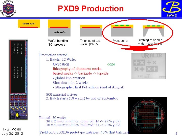
PXD 9 Production Wafer bonding SOI process Thinning of top wafer (CMP) Processing etching of handle wafer (structured) Inner outer H. -G. Moser July 25, 2012 6

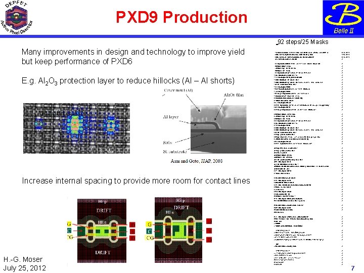
PXD 9 Production 92 steps/25 Masks RR: Many improvements in design and technology to improve yield but keep performance of PXD 6 E. g. Al 2 O 3 protection layer to reduce hillocks (Al – Al shorts) Inner outer Increase internal spacing to provide more room for contact lines 1 Feuchte Oxidation, fox 2 -950, 90 nm, davor DCE-clean, evtl. trocken in MPI 1 -4 09. 07. 2012 2 Litho ALIP neu, justiert auf vergra. ALIB, MA-IR, p-Seite 16. 07. 2012 3 Litho ALIN neu + DWL-Wafernummern, MA-VR auf ALIP 23. 07. 2012 4 Th. Oxid durchätzen, beidseitig x 5 2. Implantation ND 0 N, P 500 ke. V, 1 E 11 cm-2, n-Seite, unmaskiert x 6 LPCVD-Nitrid 1, 20 nm x 7 LPCVD-Poly 1, 550°C, 600 nm x 8 LPCVD-LTO 1, 105 nm x 9 3. Implantation Poly 1, n-Seite, P 140 ke. V, 8 E 15 cm-2 x 10 Rekristallisation, EANN-900, 1 h x 11 2. Lithographie PO 1 N, justiert auf ALIN x 12 Strukturierung LTO 1 n-Seite, SEZ x 13 Strukturierung Poly 1 n-Seite, SEZ, defreckle (30% + 30 sek defreckle) x 14 LTO 1 beidseitig abätzen, SEZ x 15 3. Lithographie PSHN x 16 4. P-Kanal Implantation, 30 ke. V, 1. 5 E 12, Dualmode x 17 4. Lithographie PDPN x 18 5. Deep P-Implantation, B 210 ke. V, 1. 5 E 12 cm-2 x 19 Oxidation Poly 1, FOX 2 -900, 215 nm x 20 Oxinitridschicht entfernen, 2 min HF-Dip x 21 Nitrid 1 durchätzen, n-Seite x 22 7. Lithographie NOXN x 23 8. N+ Implantation, As 180 ke. V, 7 E 14, Quadmode, Strombegrenzung (300µA)! x 24 5. Lithographie ND 1 N x 25 6. Deep N-Implantation, P 500 ke. V, 8 E 11 cm-2, Dualmode? x 26 LPCVD-Nitrid 2, 730°C, 30 nm x 27 LPCVD-Poly 2, 550°C, 500 nm x 28 LPCVD-LTO 2, 105 nm x 29 9. Implantation Poly 2, n-Seite, P 140 ke. V, 8 E 15 cm-2 x 30 Rekristallisation, EANN-900, 1 h x 31 8. Lithographie PO 2 N x 32 Strukturierung LTO 2 n-Seite, SEZ x 33 Strukturierung Poly 2 n-Seite, SEZ, defreckle (30% + 30 sek defreckle) x 34 LTO 2 beidseitig abätzen, SEZ x 35 Poly 2, p-Seite abätzen, SEZ x 36 Poly 2 FOX 2 -900, 215 nm? , evtl. wird die POXN vorgezogen! Rar x 37 Nitrid 2 durchätzen, beidseitig, davor 2 min HF-Dip x 38 9. Lithographie POXN x 39 8. P+ Implantation, B 25 ke. V, 1 E 15 cm-2, Quadmode!! x 40 Polyoxid 1 p-Seite abätzen, SEZ x 41 Poly 1 p-Seite abätzen, SEZ x 42 defreckle p-Seite x 43 LPCVD-Nitrid 3, d=30 nm x 44 LPCVD-LTO 3, d=300 nm x 45 LTO 3 abätzen ganzflächig, p-Seite, SEZ x 46 10. Lithographie NITN x 47 LTO 3 strukturieren, n-Seite, SAT 1 x 48 Nitrid beidseitig durchätzen, n-Seite Nitrid 3, p-Seite Nitrid 1+3 -> th. Ox liegt frei x 49 NITDANN+H 2 T-450 x 50 11. Lithographie CO 1 N x 51 Oxide öffnen, n-Seite x 52 Metallisierung hot alu, n-Seite x 53 12. Lithographie AL 1 N x 54 Hotalu strukturieren n-Seite x 55 13. Litho FRECN (invertierte und vergrößerte KO 1 N) x 56 Defreckle-etch, n-Seite x 57 El. Messen x 58 14. Lithographie AOXN x 59 Aluoxidation HOT-DI x 60 LPCVD-LTO 4 600/1000 nm? x 61 15. Lithographie KO 2 N, justiert auf al 1 n x 62 LTO 4 strukturieren, n-Seite, SAT 2 -padetch x 63 Metallisierung cold alu, n-Seite, softetch! x 64 16. Lithographie AL 2 N x 65 Alu 2 strukturieren n-Seite x 66 El. Messen 67 17. Lithographie WINP, p-Seite, justiert auf ALIP x 68 600 -1000 nm LTO 4 + 85 nm th. Oxid durchätzen, p-Seite x 69 H 2 T-400 x 70 BCBN x 71 BCBP, als Schutz für die TMAH-Ätzung x Entwicklungslabor: x 72 Waferholder n-Seite, TMAH-Ätzung p-Seite x 73 8. Lithographie KONP, p-Seite, MA Justage auf ALIP x 74 Therm. Oxid p-Seite durchätzen x 75 Sputtervorreinigung: Schutzlack n-Seite, HF-Dip 60 sek, LM-Reinigung x RR: 76 Metallisierung cold alu, p-Seite Entwicklungslabor: H. -G. Moser July 25, 2012 x x 77 12. Lithographie ALUP, MA justiert auf ALIP x 78 Alu strukturieren p-Seite x 79 H 2 T-320, davor + danach el. Messen x 80 Endreinigung, Endkontrolle x 81 bcbn/bcbp? x 92 cutn/cutp x 7

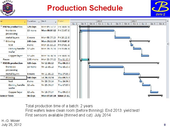
Production Schedule Total production time of a batch: 2 years First wafers leave clean room (before thinning): End 2013: yield test! First sensors available (thinned and cut): July 2014 H. -G. Moser July 25, 2012 8

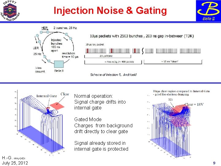
Injection Noise & Gating Normal operation: Signal charge drifts into internal gate Gated Mode Charges from background drift directly to clear gate Signal already stored in internal gate is protected H. -G. Moser July 25, 2012 9

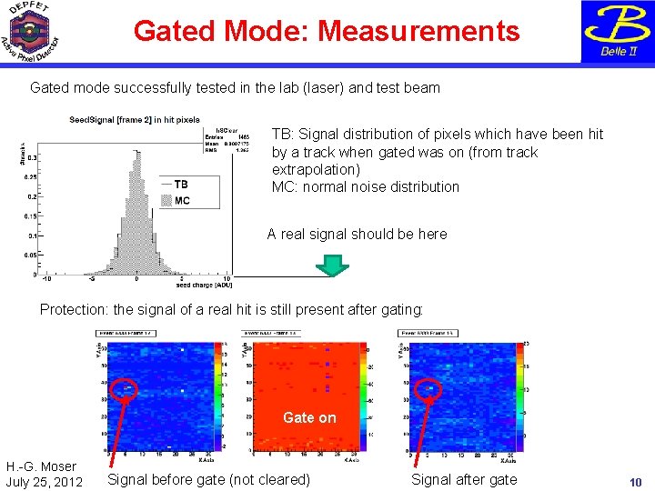
Gated Mode: Measurements Gated mode successfully tested in the lab (laser) and test beam TB: Signal distribution of pixels which have been hit by a track when gated was on (from track extrapolation) MC: normal noise distribution A real signal should be here Protection: the signal of a real hit is still present after gating: Gate on H. -G. Moser July 25, 2012 Signal before gate (not cleared) Signal after gate 10

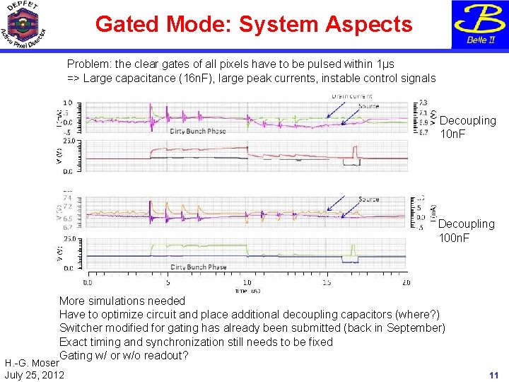
Gated Mode: System Aspects Problem: the clear gates of all pixels have to be pulsed within 1µs => Large capacitance (16 n. F), large peak currents, instable control signals Decoupling 10 n. F Decoupling 100 n. F More simulations needed Have to optimize circuit and place additional decoupling capacitors (where? ) Switcher modified for gating has already been submitted (back in September) Exact timing and synchronization still needs to be fixed Gating w/ or w/o readout? H. -G. Moser July 25, 2012 11

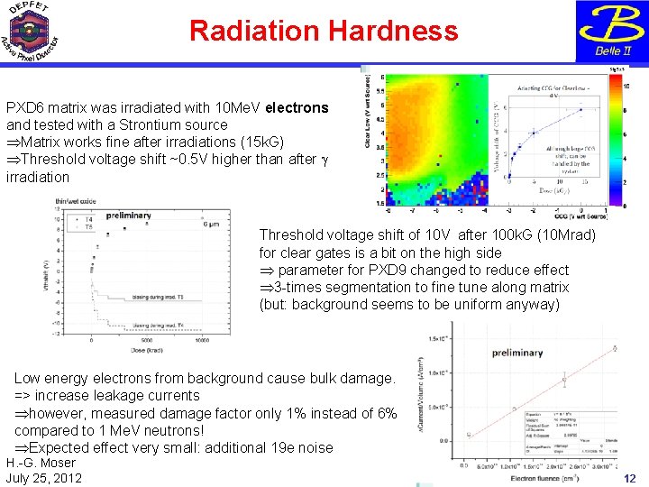
Radiation Hardness PXD 6 matrix was irradiated with 10 Me. V electrons and tested with a Strontium source ÞMatrix works fine after irradiations (15 k. G) ÞThreshold voltage shift ~0. 5 V higher than after g irradiation Threshold voltage shift of 10 V after 100 k. G (10 Mrad) for clear gates is a bit on the high side Þ parameter for PXD 9 changed to reduce effect Þ 3 -times segmentation to fine tune along matrix (but: background seems to be uniform anyway) Low energy electrons from background cause bulk damage. => increase leakage currents Þhowever, measured damage factor only 1% instead of 6% compared to 1 Me. V neutrons! ÞExpected effect very small: additional 19 e noise H. -G. Moser July 25, 2012 12

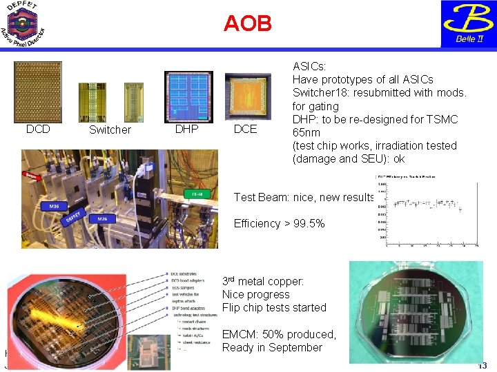
AOB DCD Switcher DHP DCE ASICs: Have prototypes of all ASICs Switcher 18: resubmitted with mods. for gating DHP: to be re-designed for TSMC 65 nm (test chip works, irradiation tested (damage and SEU): ok Test Beam: nice, new results Efficiency > 99. 5% 3 rd metal copper: Nice progress Flip chip tests started H. -G. Moser July 25, 2012 EMCM: 50% produced, Ready in September 13

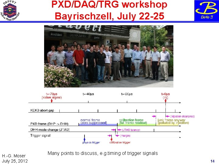
PXD/DAQ/TRG workshop Bayrischzell, July 22 -25 H. -G. Moser July 25, 2012 Many points to discuss, e. g. timing of trigger signals 14

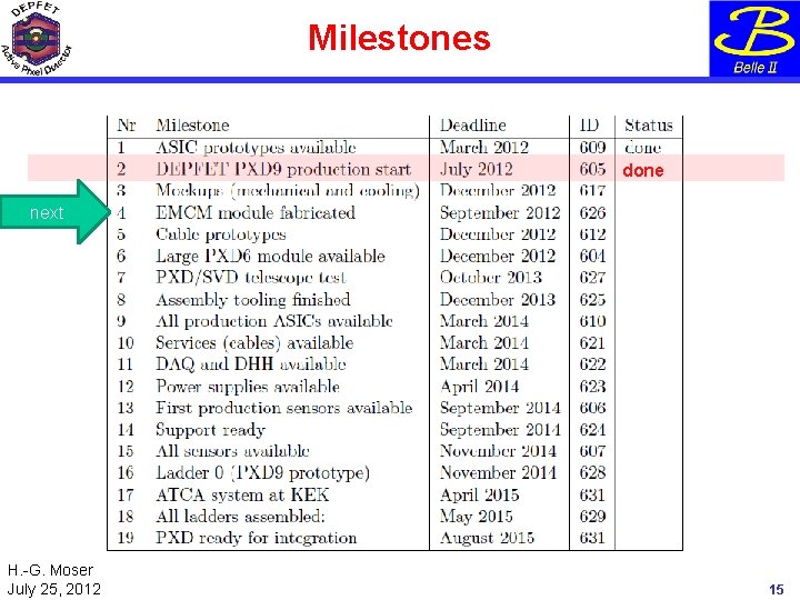
Milestones done next H. -G. Moser July 25, 2012 15

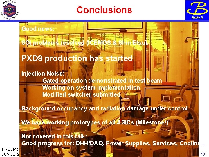
Conclusions Good news: SOI problems resolved (ICEMOS & Shin Etsu). PXD 9 production has started Injection Noise: Gated operation demonstrated in test beam Working on system implementation Modified switcher submitted Background occupancy and radiation damage under control We have working prototypes of all ASICs (Milestone!) Not covered in this talk: Good progress for: DHH/DAQ, Power Supplies, Services, Cooling … H. -G. Moser July 25, 2012 16