PWM Mode PWM Mode In Pulse Width Modulation

- Slides: 7

PWM Mode

PWM Mode In Pulse Width Modulation mode, the CCPx pin produces up to a 10 -bit resolution PWM output. Ø Since the CCP 1 pin is multiplexed with the PORTC data latch, the TRISC<2> bit must be cleared to make the CCP 1 pin an output Ø A PWM output has a time-base (period) and a time that the output stays high (duty cycle). The frequency of the PWM is the inverse of the period (1/period). Ø

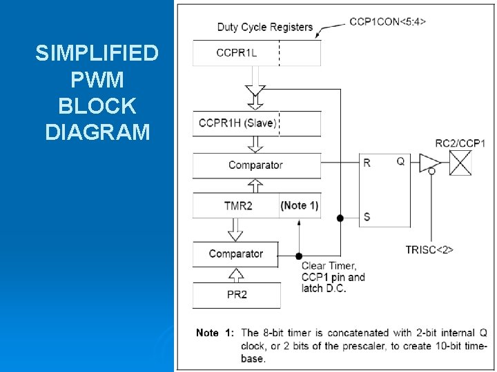
SIMPLIFIED PWM BLOCK DIAGRAM

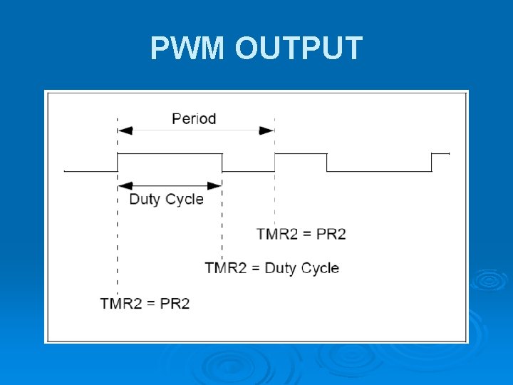
PWM OUTPUT

PWM PERIOD The PWM period is specified by writing to the PR 2 register. Ø The PWM period can be calculated using the following formula: Ø l PWM period = [(PR 2) + 1] • 4 • TOSC • (TMR 2 prescale value) PWM frequency is defined as 1 / [PWM period]. Ø When TMR 2 is equal to PR 2, the following three events occur on the next increment cycle: Ø l l Ø TMR 2 is cleared The CCP 1 pin is set (exception: if PWM duty cycle = 0%, the CCP 1 pin will not be set) The PWM duty cycle is latched from CCPR 1 L into CCPR 1 H

PWM DUTY CYCLE The PWM duty cycle is specified by writing to the CCPR 1 L register and to the CCP 1 CON<5: 4> bits. Up to 10 -bit resolution is available. Ø The following equation is used to calculate the PWM duty cycle in time: Ø l PWM duty cycle =(CCPR 1 L: CCP 1 CON<5: 4>) • TOSC • (TMR 2 prescale value) In PWM mode, CCPR 1 H is a read-only register. Ø When the CCPR 1 H and 2 -bit latch match TMR 2, concatenated with an internal 2 -bit Q clock, or 2 bits of the TMR 2 prescaler, the CCP 1 pin is cleared. Ø

SETUP FOR PWM OPERATION 1. Set the PWM period by writing to the PR 2 register. 2. Set the PWM duty cycle by writing to the CCPR 1 L register and CCP 1 CON<5: 4> bits. 3. Make the CCP 1 pin an output by clearing the TRISC<2> bit. 4. Set the TMR 2 prescale value and enable Timer 2 by writing to T 2 CON. 5. Configure the CCP 1 module for PWM operation.