pwell Formation Figure 9 9 STI Trench Etch


 LI : Local Interconnection")


 Photo courtesy of Advanced Micro")

- Slides: 27
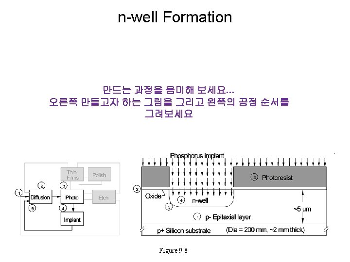
p-well Formation Figure 9. 9
STI Trench Etch Figure 9. 10
STI Oxide Fill 구멍 판 곳을 채우는 작업 Figure 9. 11
STI Formation Figure 9. 12
Poly Gate Structure Process Figure 9. 13
n- LDD Implant Figure 9. 14
p- LDD Implant Figure 9. 15
Side Wall Spacer Formation Figure 9. 16
n+ Source/Drain Implant Figure 9. 17
p+ Source/Drain Implant Figure 9. 18
Contact Formation Figure 9. 19
LI Oxide as a Dielectric for Inlaid LI Metal (Damascene) LI : Local Interconnection Figure 9. 20
LI Oxide Dielectric Formation Figure 9. 21
LI Metal Formation Figure 9. 22
Via-1 Formation Figure 9. 23
Plug-1 Formation Figure 9. 24
SEM Micrographs of Polysilicon, Tungsten LI and Tungsten Plugs Tungsten LI Polysilicon Tungsten plug Mag. 17, 000 X Micrograph courtesy of Integrated Circuit Engineering Photo 9. 4
Metal-1 Interconnect Formation Figure 9. 25
SEM Micrographs of First Metal Layer over First Set of Tungsten Vias Ti. N metal cap Metal 1, Al Tungsten plug Mag. 17, 000 X Micrograph courtesy of Integrated Circuit Engineering Photo 9. 5
Via-2 Formation Figure 9. 26
Plug-2 Formation Figure 9. 27
Metal-2 Interconnect Formation Figure 9. 28
Full 0. 18 mm CMOS Cross Section Passivation layer Bonding pad metal ILD-6 ILD-5 M-4 ILD-4 M-3 ILD-3 M-2 ILD-2 M-1 Via Poly gate LI metal n+ ILD-1 p+ LI oxide p+ STI n-well n+ n+ p-well p- Epitaxial layer p+ Silicon substrate Figure 9. 29 p+
SEM Micrograph of Cross-section of AMD Microprocessor Mag. 18, 250 X Micrograph courtesy of Integrated Circuit Engineering Photo 9. 6
Wafer Electrical Test using a Micromanipulator Prober (Parametric Testing) Photo courtesy of Advanced Micro Devices Photo 9. 7
Chapter 9 Review • • • Summary Key Terms Review Questions SMT Web Site References 222 223 224