Pusat Pengajian Kejuruteraan Mikroelektronik EMT 3514 DIGITAL IC
- Slides: 12

Pusat Pengajian Kejuruteraan Mikroelektronik EMT 351/4 DIGITAL IC DESIGN Week # Switch Level Models in Verilog

MOS Transistor Technology § Switch-level modeling – More accurate than gate-level models, but less accurate than analog transistor models in analog simulation – Simulated faster than analog models – Used to represent & simulate the behavior of individual transistor in digital circuit

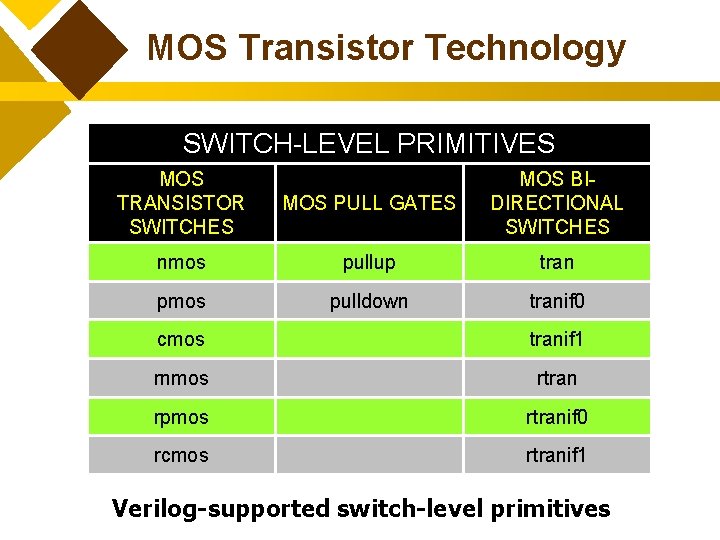
MOS Transistor Technology SWITCH-LEVEL PRIMITIVES MOS TRANSISTOR SWITCHES MOS PULL GATES MOS BIDIRECTIONAL SWITCHES nmos pullup tran pmos pulldown tranif 0 cmos tranif 1 rnmos rtran rpmos rtranif 0 rcmos rtranif 1 Verilog-supported switch-level primitives

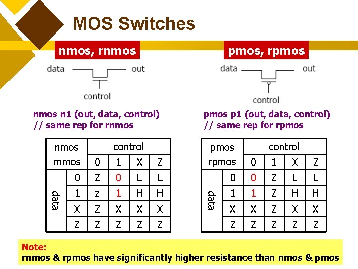
MOS Switches nmos, rnmos pmos, rpmos n 1 (out, data, control) // same rep for rnmos p 1 (out, data, control) // same rep for rpmos control 1 X 0 Z 0 1 z X Z control Z pmos rpmos 0 1 X Z L L 0 0 Z L L 1 H H 1 1 Z H H Z X X X Z Z Z Z Z data 0 data nmos rnmos Note: rnmos & rpmos have significantly higher resistance than nmos & pmos

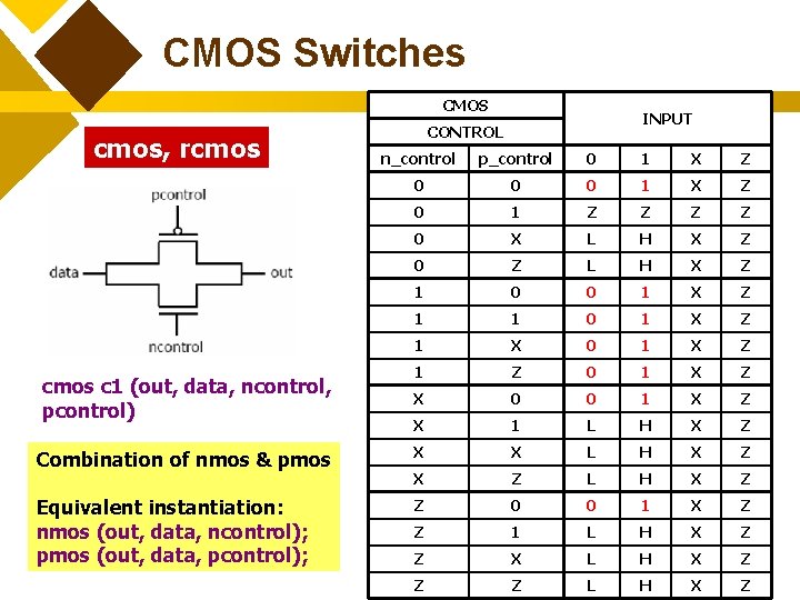
CMOS Switches CMOS cmos, rcmos INPUT CONTROL n_control p_control 0 1 X Z 0 0 0 1 X Z 0 1 Z Z 0 X L H X Z 0 Z L H X Z 1 0 0 1 X Z 1 1 0 1 X Z 1 X 0 1 X Z cmos c 1 (out, data, ncontrol, pcontrol) 1 Z 0 1 X Z X 0 0 1 X Z X 1 L H X Z Combination of nmos & pmos X X L H X Z Equivalent instantiation: nmos (out, data, ncontrol); pmos (out, data, pcontrol); Z 0 0 1 X Z Z 1 L H X Z Z X L H X Z Z Z L H X Z

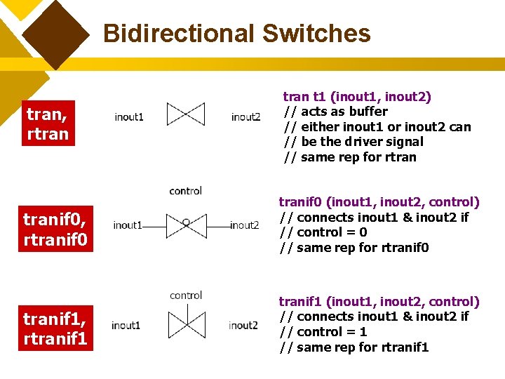
Bidirectional Switches tran, rtran t 1 (inout 1, inout 2) // acts as buffer // either inout 1 or inout 2 can // be the driver signal // same rep for rtranif 0, rtranif 0 (inout 1, inout 2, control) // connects inout 1 & inout 2 if // control = 0 // same rep for rtranif 0 tranif 1, rtranif 1 (inout 1, inout 2, control) // connects inout 1 & inout 2 if // control = 1 // same rep for rtranif 1

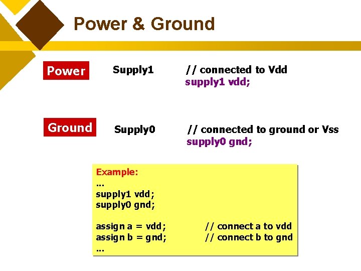
Power & Ground Power Supply 1 // connected to Vdd supply 1 vdd; Ground Supply 0 // connected to ground or Vss supply 0 gnd; Example: . . . supply 1 vdd; supply 0 gnd; assign a = vdd; assign b = gnd; . . . // connect a to vdd // connect b to gnd

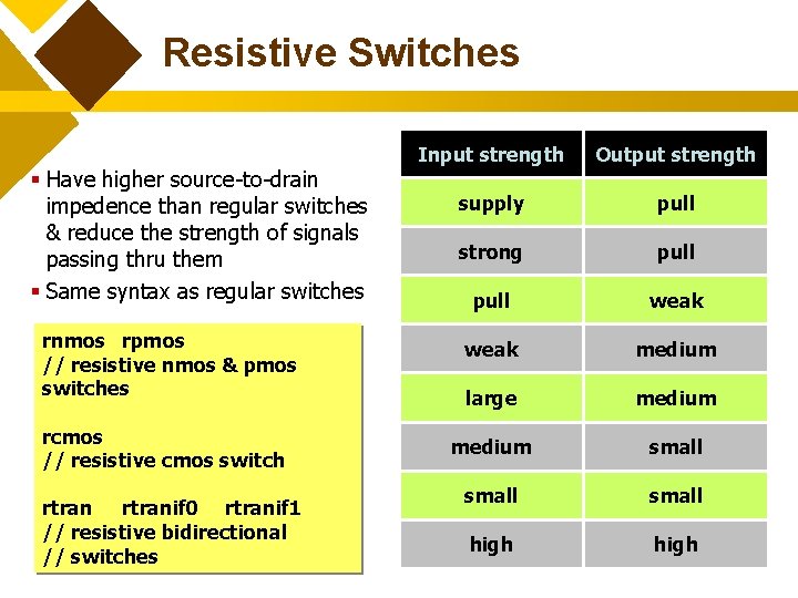
Resistive Switches § Have higher source-to-drain impedence than regular switches & reduce the strength of signals passing thru them § Same syntax as regular switches rnmos rpmos // resistive nmos & pmos switches rcmos // resistive cmos switch rtranif 0 rtranif 1 // resistive bidirectional // switches Input strength Output strength supply pull strong pull weak medium large medium small high

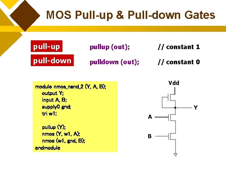
MOS Pull-up & Pull-down Gates pull-up pullup (out); // constant 1 pull-down pulldown (out); // constant 0 module nmos_nand_2 (Y, A, B); output Y; input A, B; supply 0 gnd; tri w 1; pullup (Y); nmos (Y, w 1, A); nmos (w 1, gnd, B); endmodule Vdd Y A B

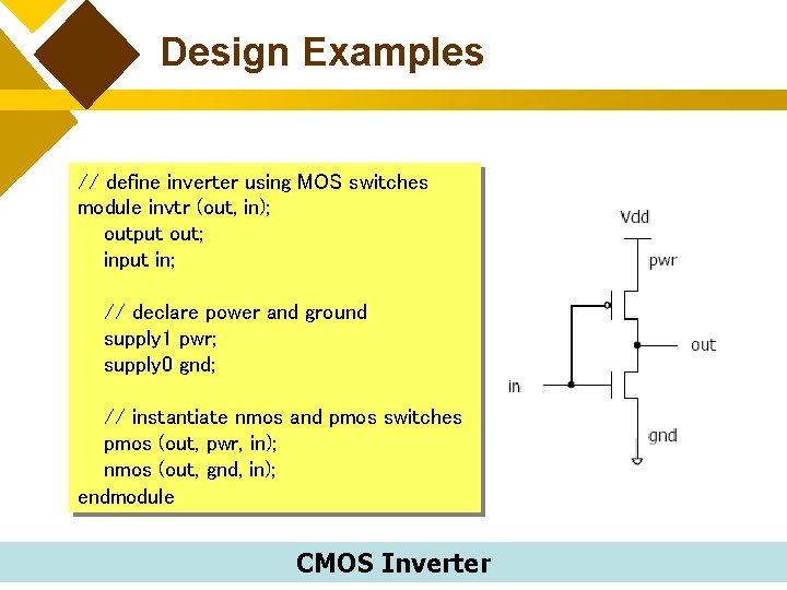
Design Examples // define inverter using MOS switches module invtr (out, in); output out; input in; // declare power and ground supply 1 pwr; supply 0 gnd; // instantiate nmos and pmos switches pmos (out, pwr, in); nmos (out, gnd, in); endmodule CMOS Inverter

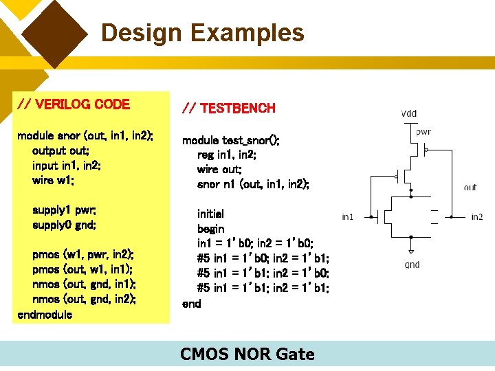
Design Examples // VERILOG CODE // TESTBENCH module snor (out, in 1, in 2); output out; input in 1, in 2; wire w 1; module test_snor(); reg in 1, in 2; wire out; snor n 1 (out, in 1, in 2); supply 1 pwr; supply 0 gnd; pmos (w 1, pwr, in 2); pmos (out, w 1, in 1); nmos (out, gnd, in 2); endmodule initial begin in 1 = 1’b 0; in 2 = 1’b 0; #5 in 1 = 1’b 0; in 2 = 1’b 1; #5 in 1 = 1’b 1; in 2 = 1’b 0; #5 in 1 = 1’b 1; in 2 = 1’b 1; end CMOS NOR Gate

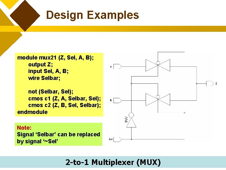
Design Examples module mux 21 (Z, Sel, A, B); output Z; input Sel, A, B; wire Selbar; not (Selbar, Sel); cmos c 1 (Z, A, Selbar, Sel); cmos c 2 (Z, B, Selbar); endmodule Note: Signal ‘Selbar’ can be replaced by signal ‘~Sel’ 2 -to-1 Multiplexer (MUX)