PUSAT PENGAJIAN DIPLOMA UNIVERSITI MALAYSIA PERLIS Uni MAP

- Slides: 68

PUSAT PENGAJIAN DIPLOMA UNIVERSITI MALAYSIA PERLIS (Uni. MAP) DNT 245 SENSORS & MEASUREMENTS Chapter 4 Signal Characteristics & Signal Conditioning Lecturer : Nor Shaifudin Bin Abdul Hamid

What is Signal? 2 In the physical world, any quantity exhibiting variation in time or variation in space is potentially a signal. In communication system, a transmitter encodes a message into signal, carried to a receiver by a communication channel. Signals are often provided by a sensor and often the original form of a signal is converted to another form of energy Example: a microphone converts an acoustic signal to a voltage waveform, and a speaker does the reverse.

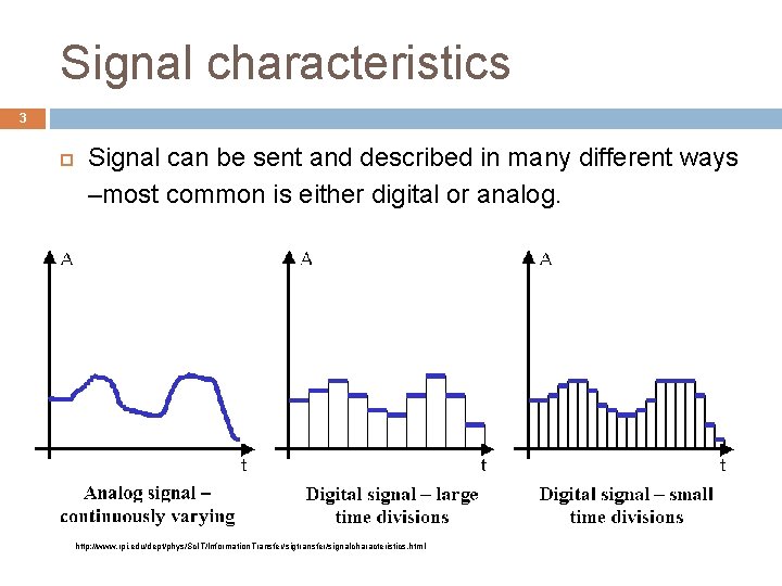
Signal characteristics 3 Signal can be sent and described in many different ways –most common is either digital or analog. http: //www. rpi. edu/dept/phys/Sc. IT/Information. Transfer/sigtransfer/signalcharacteristics. html

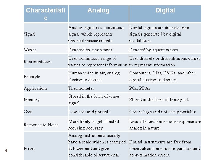
Characteristi c 4 Analog Digital Signal Analog signal is a continuous signal which represents physical measurements. Digital signals are discrete time signals generated by digital modulation. Waves Denoted by sine waves Denoted by square waves Representation Uses continuous range of Uses discrete or discontinuous values to represent information Example Human voice in air, analog electronic devices. Computers, CDs, DVDs, and other digital electronic devices. Applications Thermometer PCs, PDAs Memory Stored in the form of wave signal Stored in the form of binary bit Cost Low cost and portable Cost is high and not easily portable Response to Noise More likely to get affected reducing accuracy Less affected since noise response are analog in nature Errors Analog instruments usually have a scale which is cramped Digital instruments are free from at lower end and give observational errors like parallax and considerable observational approximation errors.

Digital vs Analog Signal 5 Digital signals are fairly immune to the imperfections of real electronic systems which tend to spoil analog signals. Digital signals can convey information with greater noise immunity, Analog signals vary continuously and their value is affected by all levels of noise. Digital signals can be processed by digital circuit components, which are cheap and easily produced in many components on a single chip Digital signals typically use less bandwidth -can cram more information (audio, video) into the same space. It is more secure. http: //digital-signal-process. blogspot. com/2011/01/advantage-of-digital-over-analog-signal. html

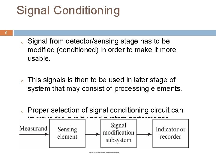
Signal Conditioning 6 o o o Signal from detector/sensing stage has to be modified (conditioned) in order to make it more usable. This signals is then to be used in later stage of system that may consist of processing elements. Proper selection of signal conditioning circuit can improve the quality and system performance.

7 Functions of Signal Conditioners There are many possible functions of signal conditioning stage: � Amplification � Attenuation � Filtering � Differentiation � Integration � Linearization � Converting a resistance to voltage signal � Converting a current signal to voltage signal � Etc

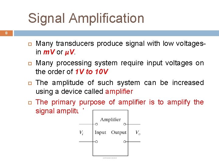
Signal Amplification 8 Many transducers produce signal with low voltagesin m. V or μV. Many processing system require input voltages on the order of 1 V to 10 V The amplitude of such system can be increased using a device called amplifier The primary purpose of amplifier is to amplify the signal amplitude.

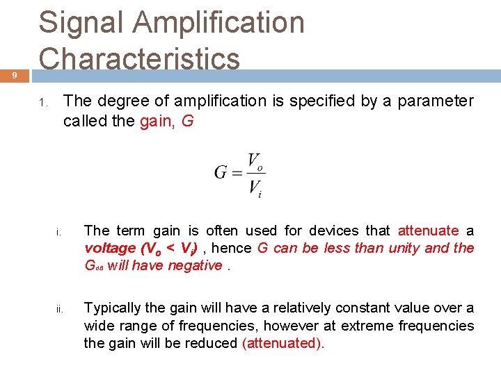
9 Signal Amplification Characteristics The degree of amplification is specified by a parameter called the gain, G 1. i. The term gain is often used for devices that attenuate a voltage (Vo < Vi) , hence G can be less than unity and the Gd. B will have negative. ii. Typically the gain will have a relatively constant value over a wide range of frequencies, however at extreme frequencies the gain will be reduced (attenuated).

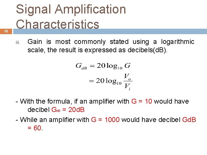
10 Signal Amplification Characteristics iii. Gain is most commonly stated using a logarithmic scale, the result is expressed as decibels(d. B). - With the formula, if an amplifier with G = 10 would have decibel Gd. B = 20 d. B - While an amplifier with G = 1000 would have decibel Gd. B = 60.

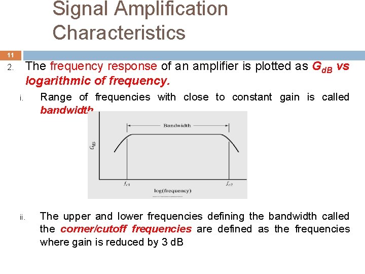
Signal Amplification Characteristics 11 The frequency response of an amplifier is plotted as Gd. B vs logarithmic of frequency. 2. i. Range of frequencies with close to constant gain is called bandwidth. ii. The upper and lower frequencies defining the bandwidth called the corner/cutoff frequencies are defined as the frequencies where gain is reduced by 3 d. B

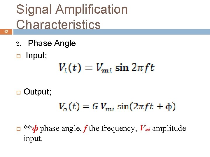
12 Signal Amplification Characteristics 3. Phase Angle Input; Output; **ф phase angle, f the frequency, Vmi amplitude input.

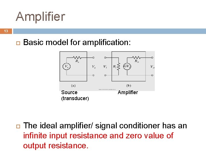
Amplifier 13 Basic model for amplification: Source (transducer) Amplifier The ideal amplifier/ signal conditioner has an infinite input resistance and zero value of output resistance.

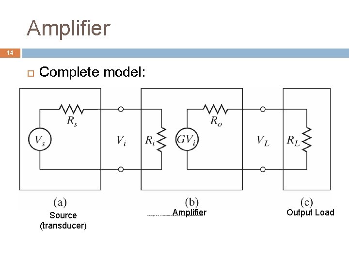
Amplifier 14 Complete model: Source (transducer) Amplifier Output Load

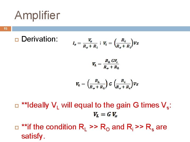
Amplifier 15 Derivation: **Ideally VL will equal to the gain G times Vs: **if the condition RL >> RO and Ri >> Rs are satisfy.

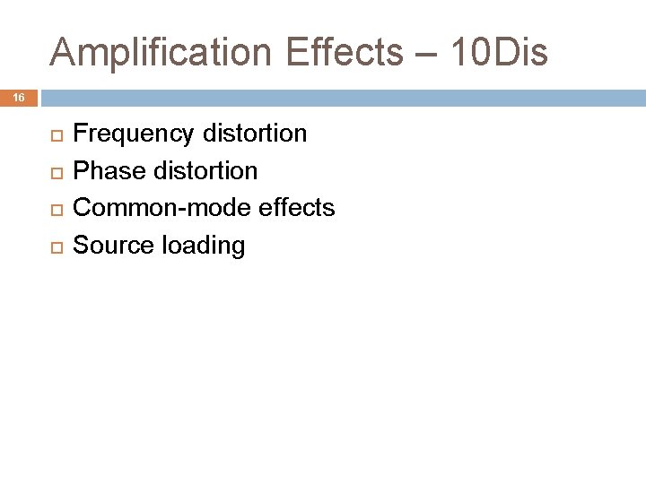
Amplification Effects – 10 Dis 16 Frequency distortion Phase distortion Common-mode effects Source loading

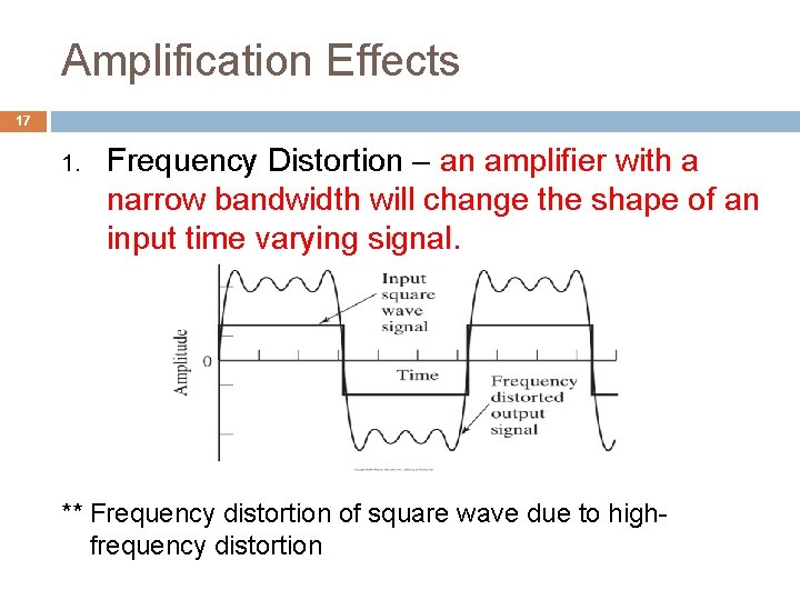
Amplification Effects 17 1. Frequency Distortion – an amplifier with a narrow bandwidth will change the shape of an input time varying signal. ** Frequency distortion of square wave due to highfrequency distortion

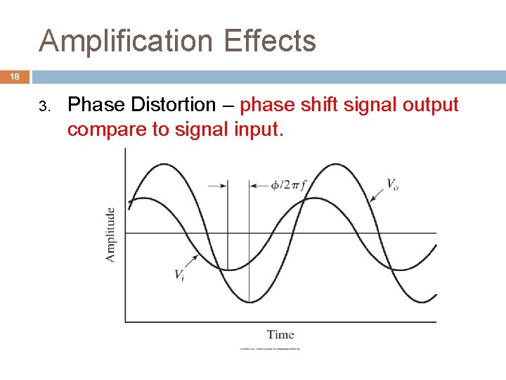
Amplification Effects 18 3. Phase Distortion – phase shift signal output compare to signal input.

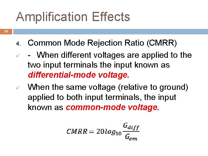
Amplification Effects 19 4. ü ü Common Mode Rejection Ratio (CMRR) - When different voltages are applied to the two input terminals the input known as differential-mode voltage. When the same voltage (relative to ground) applied to both input terminals, the input known as common-mode voltage.

Amplification Effects 20 ü ü An ideal instrumentation amplifier will produce an output in response to differential-mode voltages and will not produce an output in response to common-mode voltages. Real amplifiers will produce an output response for both condition but for differentialmode voltages will be much larger.

Amplification Effects 21 5. Source loading error – input loading & output loading caused by using many other signalconditioning devices.

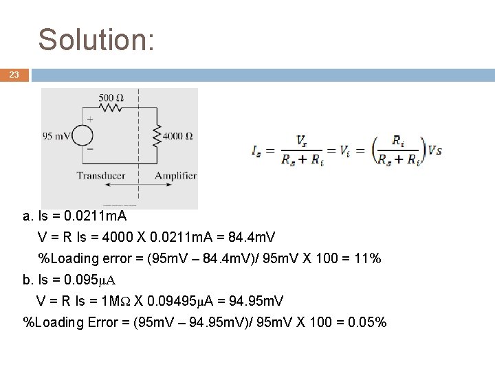
Example: 22 A force-measuring transducer has an opencircuit output voltage of 95 m. V and an output impedance of 500Ω. To amplify the signal voltage, it is connected to an amplifier with a gain of 10. Estimate the input loading error if the amplifier has an input impedance of: a. 4 kΩ or b. 1 MΩ

Solution: 23 a. Is = 0. 0211 m. A V = R Is = 4000 X 0. 0211 m. A = 84. 4 m. V %Loading error = (95 m. V – 84. 4 m. V)/ 95 m. V X 100 = 11% b. Is = 0. 095μA V = R Is = 1 MΩ X 0. 09495μA = 94. 95 m. V %Loading Error = (95 m. V – 94. 95 m. V)/ 95 m. V X 100 = 0. 05%

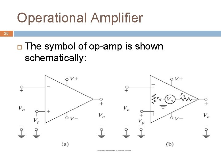
Amplifiers - Operational Amplifier 24 Operational amplifier (op-amp) is a high gain, low cost, integrated circuit designed to amplify signals. Can be used to performs an important functions for signal conditioning and processing like isolation, addition, inversion, multiplication, subtraction and division, integration or differentiation.

Operational Amplifier 25 The symbol of op-amp is shown schematically:

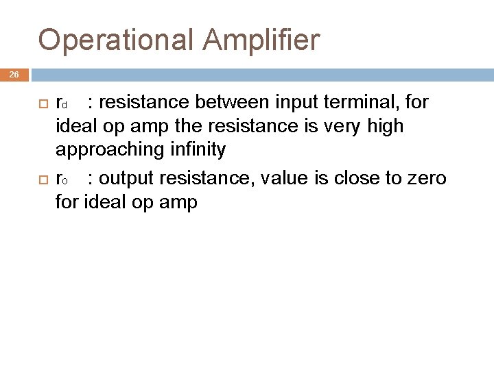
Operational Amplifier 26 rd : resistance between input terminal, for ideal op amp the resistance is very high approaching infinity ro : output resistance, value is close to zero for ideal op amp

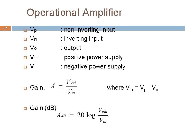
Operational Amplifier 27 Vp Vn Vo V+ V- Gain, Gain (d. B), : non-inverting input : output : positive power supply : negative power supply where Vin = Vp - Vn

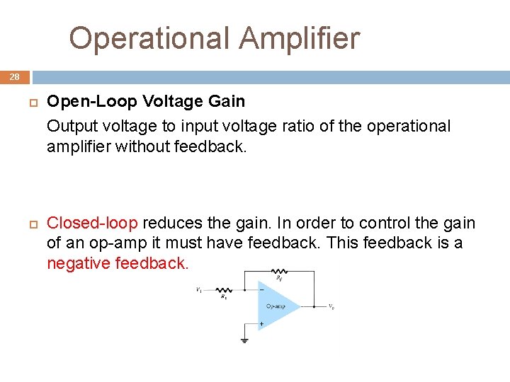
Operational Amplifier 28 Open-Loop Voltage Gain Output voltage to input voltage ratio of the operational amplifier without feedback. Closed-loop reduces the gain. In order to control the gain of an op-amp it must have feedback. This feedback is a negative feedback.

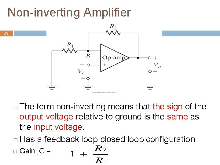
Non-inverting Amplifier 29 The term non-inverting means that the sign of the output voltage relative to ground is the same as the input voltage. � Has a feedback loop-closed loop configuration � � Gain , G =

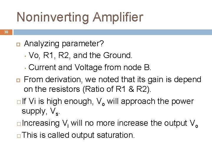
Noninverting Amplifier 30 Analyzing parameter? • Vo, R 1, R 2, and the Ground. • Current and Voltage from node B. From derivation, we noted that its gain is depend on the resistors (Ratio of R 1 & R 2). � If Vi is high enough, Vo will approach the power supply, Vs. � Increasing Vi will no more increase the output Vo � This is called output saturation.

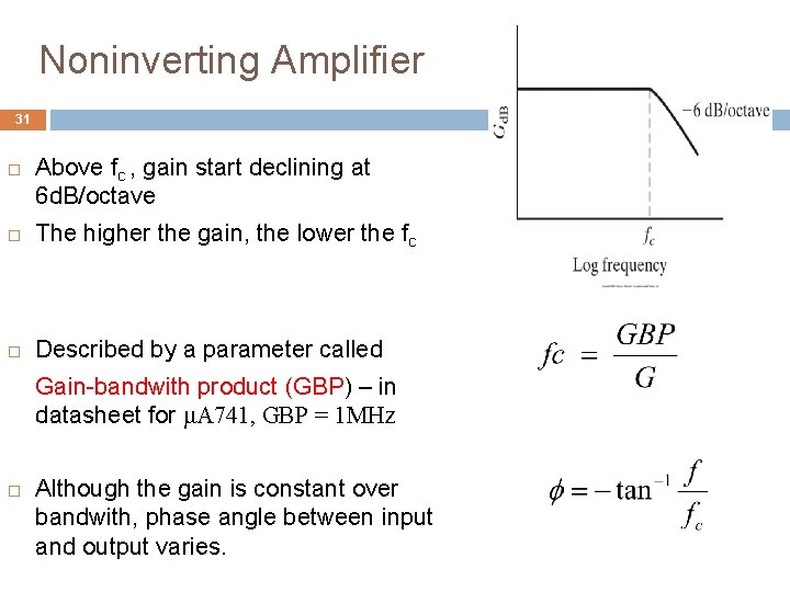
Noninverting Amplifier 31 Above fc , gain start declining at 6 d. B/octave The higher the gain, the lower the fc Described by a parameter called Gain-bandwith product (GBP) – in datasheet for μA 741, GBP = 1 MHz Although the gain is constant over bandwith, phase angle between input and output varies.

Example: 32 Specify values of resistors R 1 and R 2 for noninverting op-amp 741 amplifier with a gain of 10. find the cut-off frequency and the phase shift for sinusoidal input voltage with a frequency of 10 k. Hz.

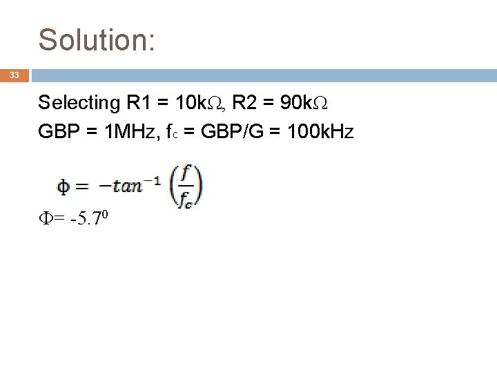
Solution: 33 Selecting R 1 = 10 kΩ, R 2 = 90 kΩ GBP = 1 MHz, fc = GBP/G = 100 k. Hz Ф= -5. 70

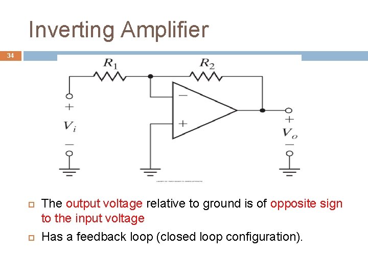
Inverting Amplifier 34 The output voltage relative to ground is of opposite sign to the input voltage Has a feedback loop (closed loop configuration).

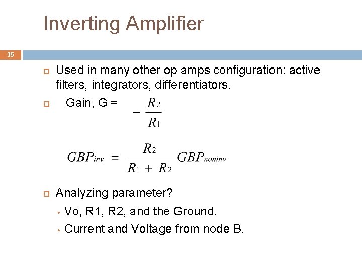
Inverting Amplifier 35 Used in many other op amps configuration: active filters, integrators, differentiators. Gain, G = Analyzing parameter? • Vo, R 1, R 2, and the Ground. • Current and Voltage from node B.

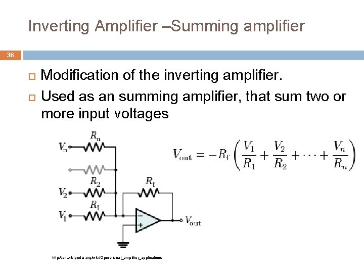
Inverting Amplifier –Summing amplifier 36 Modification of the inverting amplifier. Used as an summing amplifier, that sum two or more input voltages http: //en. wikipedia. org/wiki/Operational_amplifier_applications

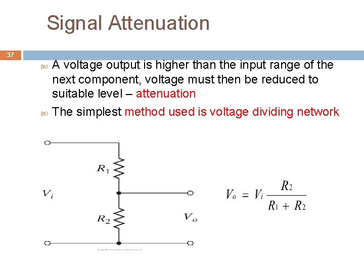
Signal Attenuation 37 A voltage output is higher than the input range of the next component, voltage must then be reduced to suitable level – attenuation The simplest method used is voltage dividing network

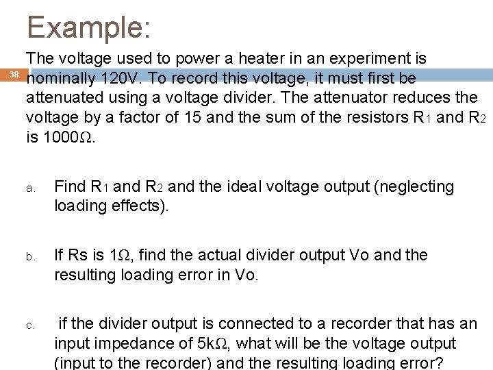
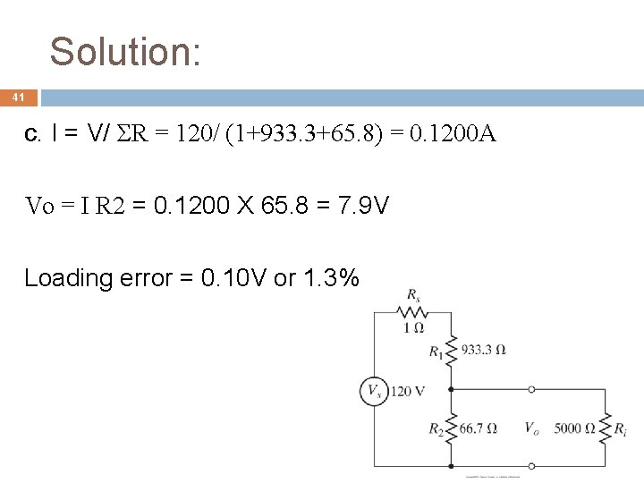
Example: 38 The voltage used to power a heater in an experiment is nominally 120 V. To record this voltage, it must first be attenuated using a voltage divider. The attenuator reduces the voltage by a factor of 15 and the sum of the resistors R 1 and R 2 is 1000Ω. a. Find R 1 and R 2 and the ideal voltage output (neglecting loading effects). b. If Rs is 1Ω, find the actual divider output Vo and the resulting loading error in Vo. c. if the divider output is connected to a recorder that has an input impedance of 5 kΩ, what will be the voltage output (input to the recorder) and the resulting loading error?

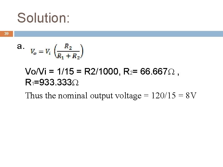
Solution: 39 a. Vo/Vi = 1/15 = R 2/1000, R 2= 66. 667Ω , R 1=933. 333Ω Thus the nominal output voltage = 120/15 = 8 V

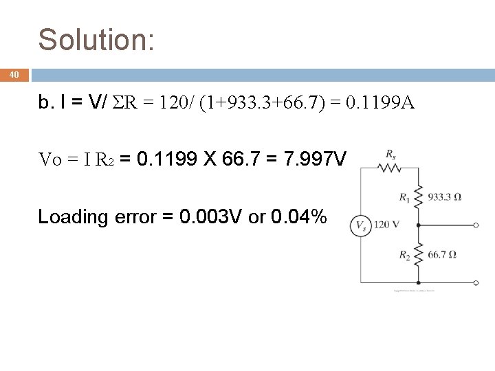
Solution: 40 b. I = V/ ΣR = 120/ (1+933. 3+66. 7) = 0. 1199 A Vo = I R 2 = 0. 1199 X 66. 7 = 7. 997 V Loading error = 0. 003 V or 0. 04%

Solution: 41 c. I = V/ ΣR = 120/ (1+933. 3+65. 8) = 0. 1200 A Vo = I R 2 = 0. 1200 X 65. 8 = 7. 9 V Loading error = 0. 10 V or 1. 3%

42 Analog signal Conditioning 12 Dis Filtering: The process to remove some of the frequencies that not necessary in many sine waves of different frequencies and amplitude with time varying voltage.

How Filtering is Important: 43 1. To filter spurious noise such as 60 Hz power line noise imposed on the signal. 2. To avoid aliasing, in data acquisition system samples the signal at discrete times rather than continuously.

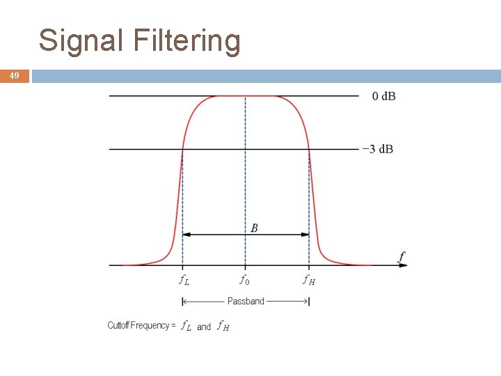
Filter: 44 § § Filter is a circuit/device that passes electrical signals at certain frequencies while attenuates or rejects others. Consist at least one pass band - range of frequencies that are allowed to pass through the filter Cut-off frequencies , fc - is the frequency beyond which the filter will not pass signalsusually measured at a specific attenuation such as 3 d. B.

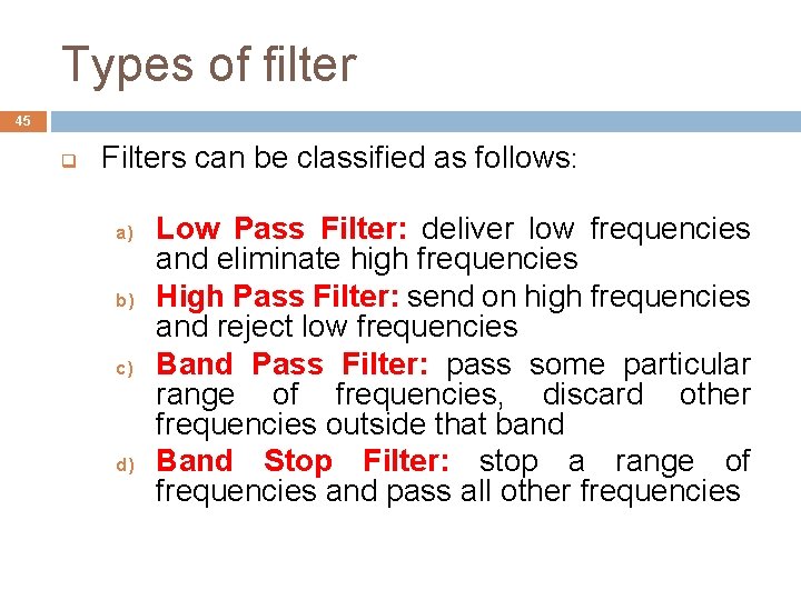
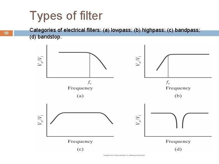
Types of filter 45 q Filters can be classified as follows: a) b) c) d) Low Pass Filter: deliver low frequencies and eliminate high frequencies High Pass Filter: send on high frequencies and reject low frequencies Band Pass Filter: pass some particular range of frequencies, discard other frequencies outside that band Band Stop Filter: stop a range of frequencies and pass all other frequencies

Classes of Filters: 46 1. 2. 3. 4. Butterworth Chebyshev Elliptic Bessel

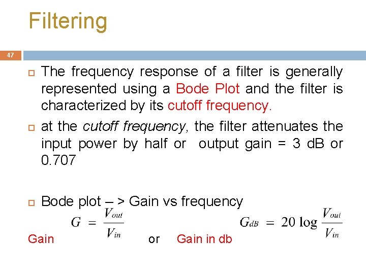
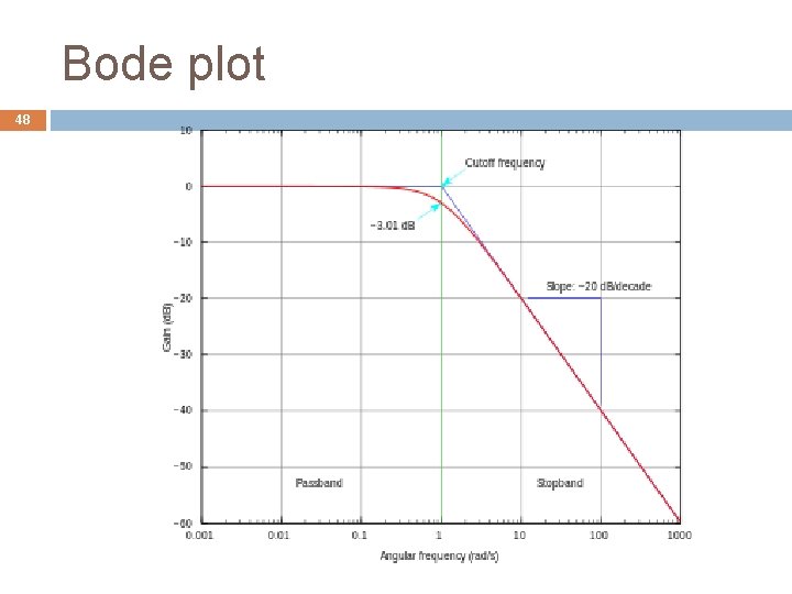
Filtering 47 The frequency response of a filter is generally represented using a Bode Plot and the filter is characterized by its cutoff frequency. at the cutoff frequency, the filter attenuates the input power by half or output gain = 3 d. B or 0. 707 Bode plot – > Gain vs frequency Gain or Gain in db

Bode plot 48

Signal Filtering 49

Types of filter 50 Categories of electrical filters: (a) lowpass; (b) highpass; (c) bandpass; (d) bandstop.

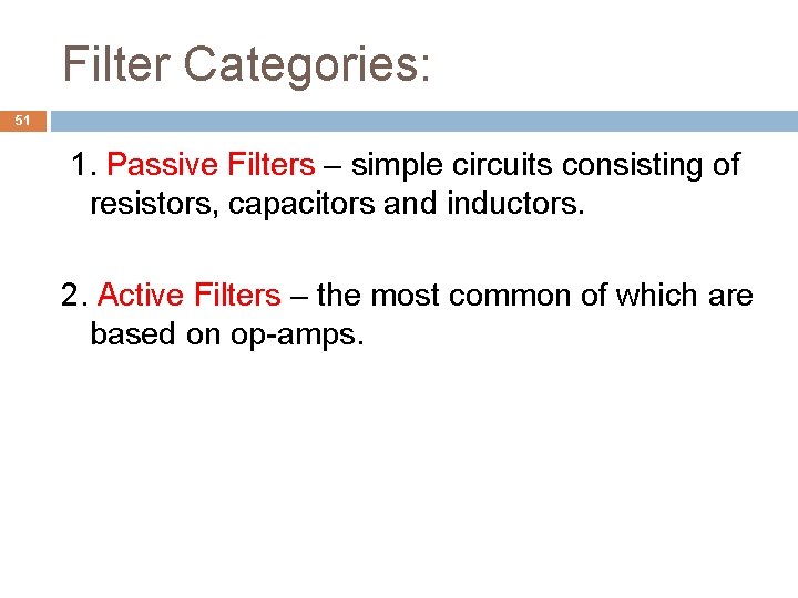
Filter Categories: 51 1. Passive Filters – simple circuits consisting of resistors, capacitors and inductors. 2. Active Filters – the most common of which are based on op-amps.

52 Passive Filters:

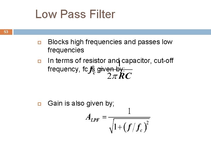
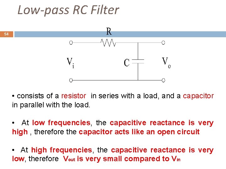
Low Pass Filter 53 Blocks high frequencies and passes low frequencies In terms of resistor and capacitor, cut-off frequency, fc is given by: Gain is also given by;

Low-pass RC Filter 54 • consists of a resistor in series with a load, and a capacitor in parallel with the load. • At low frequencies, the capacitive reactance is very high , therefore the capacitor acts like an open circuit • At high frequencies, the capacitive reactance is very low, therefore Vout is very small compared to Vin

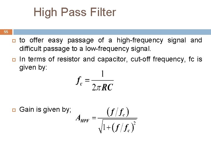
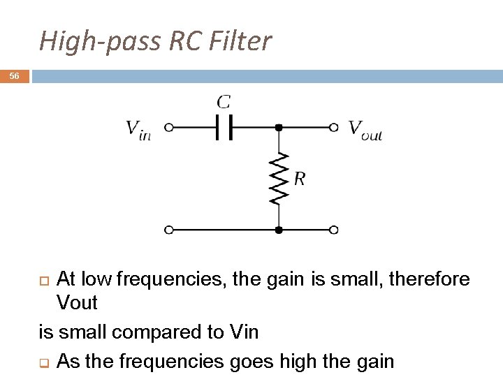
High Pass Filter 55 to offer easy passage of a high-frequency signal and difficult passage to a low-frequency signal. In terms of resistor and capacitor, cut-off frequency, fc is given by: Gain is given by;

High-pass RC Filter 56 At low frequencies, the gain is small, therefore Vout is small compared to Vin q As the frequencies goes high the gain

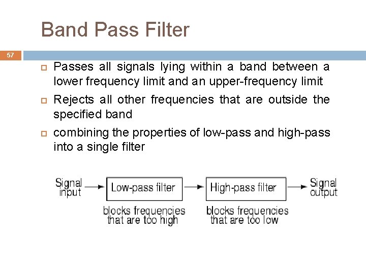
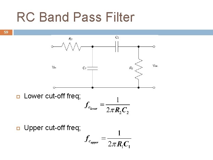
Band Pass Filter 57 Passes all signals lying within a band between a lower frequency limit and an upper-frequency limit Rejects all other frequencies that are outside the specified band combining the properties of low-pass and high-pass into a single filter

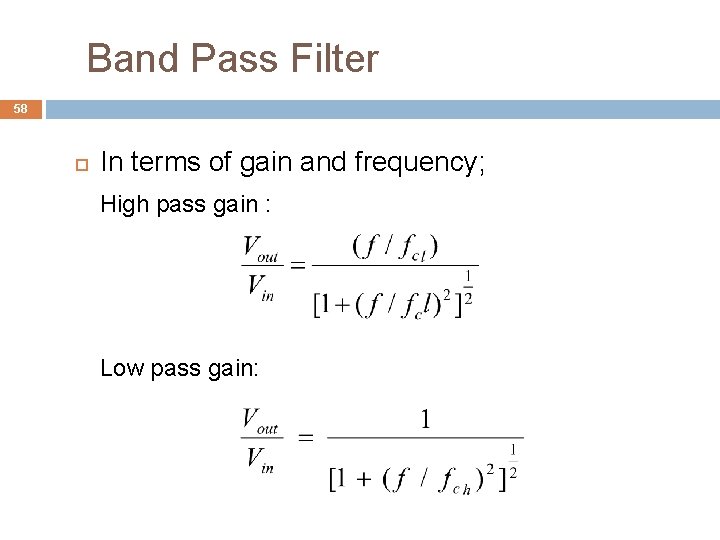
Band Pass Filter 58 In terms of gain and frequency; High pass gain : Low pass gain:

RC Band Pass Filter 59 Lower cut-off freq; Upper cut-off freq;

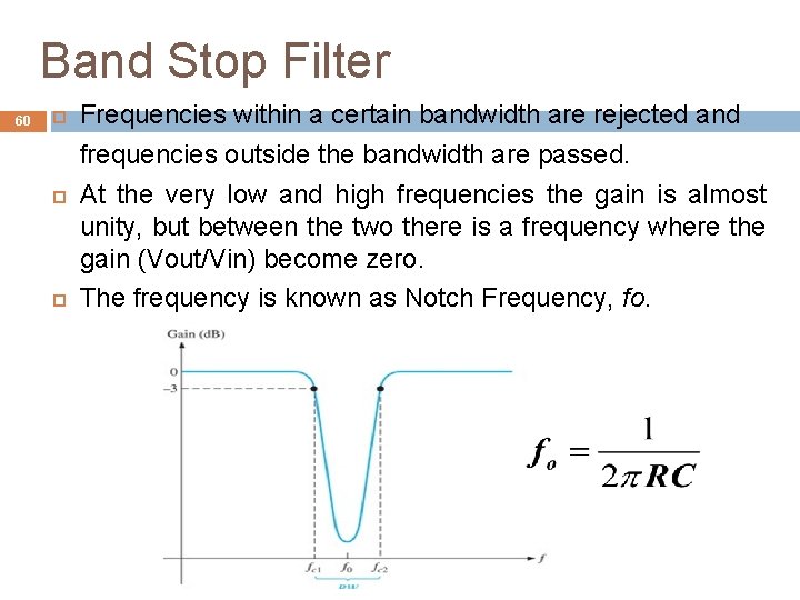
Band Stop Filter 60 Frequencies within a certain bandwidth are rejected and frequencies outside the bandwidth are passed. At the very low and high frequencies the gain is almost unity, but between the two there is a frequency where the gain (Vout/Vin) become zero. The frequency is known as Notch Frequency, fo.

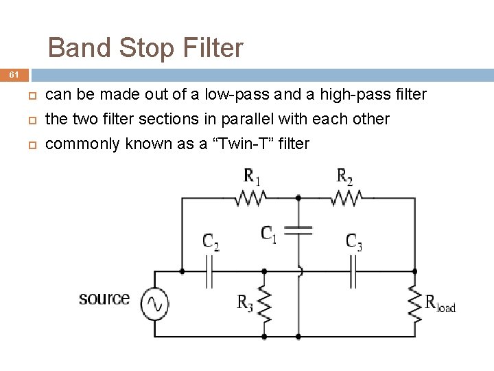
Band Stop Filter 61 can be made out of a low-pass and a high-pass filter the two filter sections in parallel with each other commonly known as a “Twin-T” filter

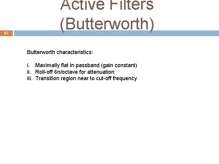
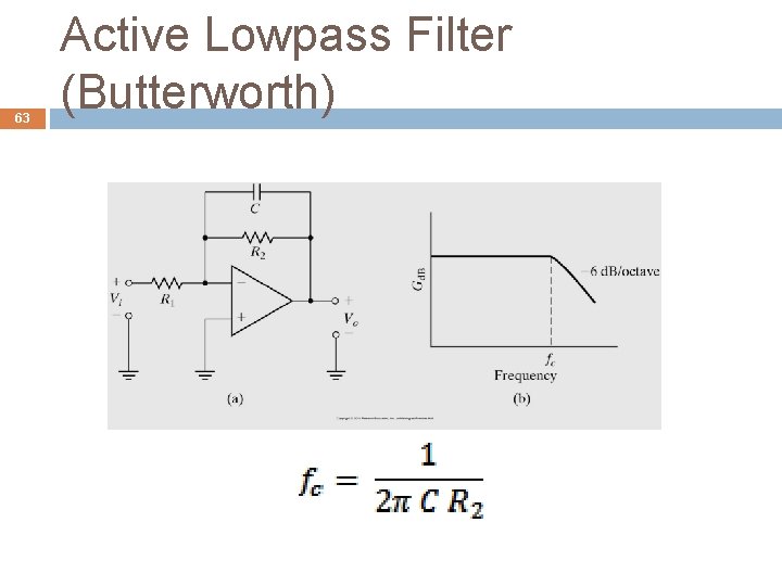
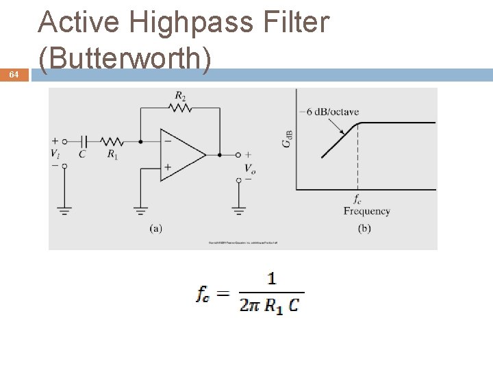
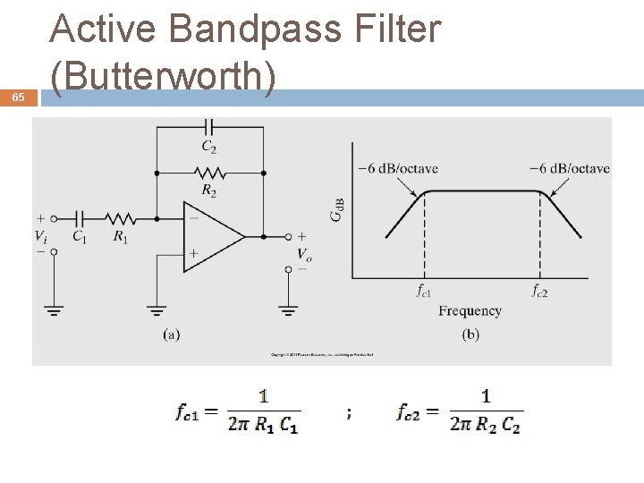
62 Active Filters (Butterworth) Butterworth characteristics: i. Maximally flat in passband (gain constant) ii. Roll-off 6 n/octave for attenuation iii. Transition region near to cut-off frequency

63 Active Lowpass Filter (Butterworth)

64 Active Highpass Filter (Butterworth)

65 Active Bandpass Filter (Butterworth)

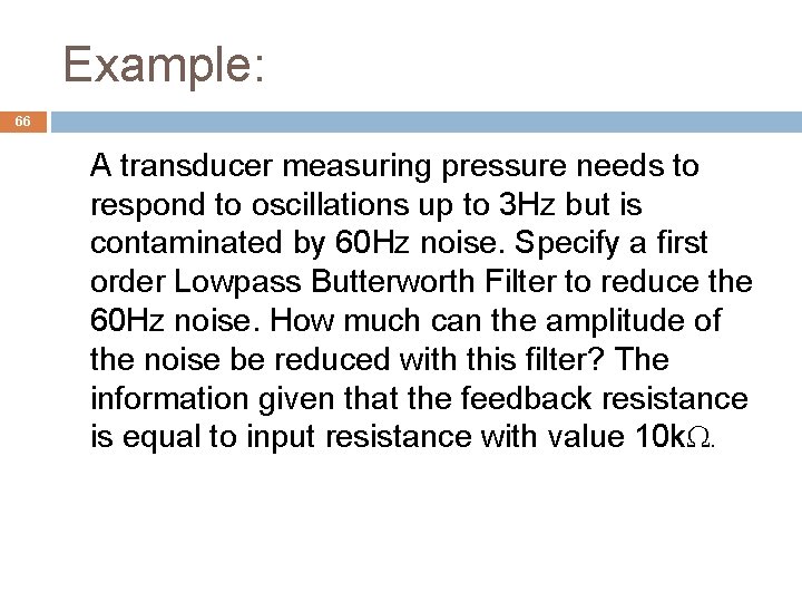
Example: 66 A transducer measuring pressure needs to respond to oscillations up to 3 Hz but is contaminated by 60 Hz noise. Specify a first order Lowpass Butterworth Filter to reduce the 60 Hz noise. How much can the amplitude of the noise be reduced with this filter? The information given that the feedback resistance is equal to input resistance with value 10 kΩ.

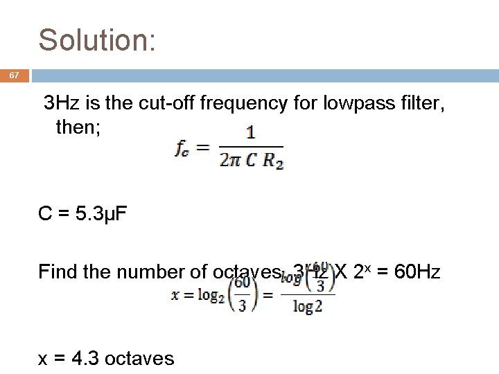
Solution: 67 3 Hz is the cut-off frequency for lowpass filter, then; C = 5. 3µF Find the number of octaves, 3 Hz X 2 x = 60 Hz x = 4. 3 octaves

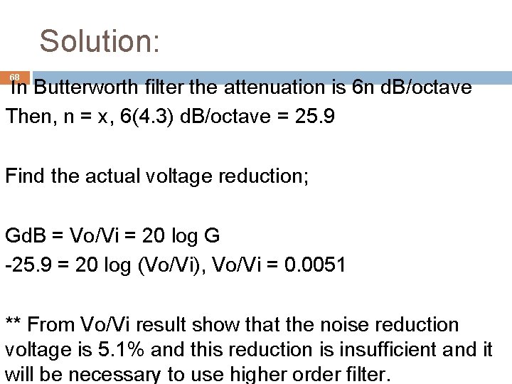
Solution: 68 In Butterworth filter the attenuation is 6 n d. B/octave Then, n = x, 6(4. 3) d. B/octave = 25. 9 Find the actual voltage reduction; Gd. B = Vo/Vi = 20 log G -25. 9 = 20 log (Vo/Vi), Vo/Vi = 0. 0051 ** From Vo/Vi result show that the noise reduction voltage is 5. 1% and this reduction is insufficient and it will be necessary to use higher order filter.