PUSAT PENGAJIAN DIPLOMA KEJURUTERAAN MEKATRONIK DNT 125 ANALOGUE




- Slides: 23

PUSAT PENGAJIAN DIPLOMA ( KEJURUTERAAN MEKATRONIK) DNT 125 ANALOGUE ELECTRONICS Chapter 4 Small Signal Transistor Amplifier

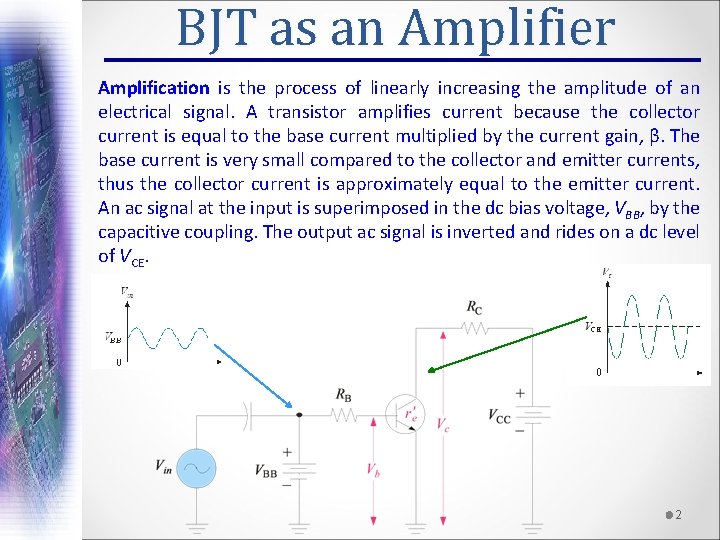
BJT as an Amplifier Amplification is the process of linearly increasing the amplitude of an electrical signal. A transistor amplifies current because the collector current is equal to the base current multiplied by the current gain, β. The base current is very small compared to the collector and emitter currents, thus the collector current is approximately equal to the emitter current. An ac signal at the input is superimposed in the dc bias voltage, VBB, by the capacitive coupling. The output ac signal is inverted and rides on a dc level of VCE. 2

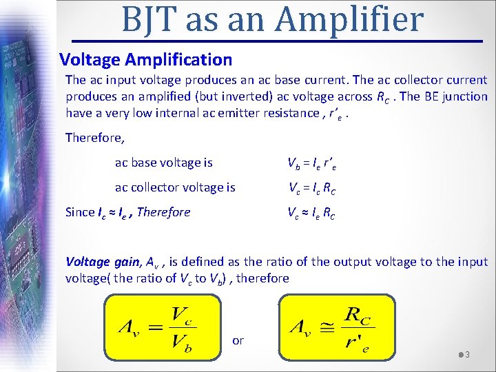
BJT as an Amplifier Voltage Amplification The ac input voltage produces an ac base current. The ac collector current produces an amplified (but inverted) ac voltage across RC. The BE junction have a very low internal ac emitter resistance , r’e. Therefore, ac base voltage is Vb = Ie r’e ac collector voltage is Vc = I c R C Since Ic ≈ Ie , Therefore Vc ≈ I e R C Voltage gain, Av , is defined as the ratio of the output voltage to the input voltage( the ratio of Vc to Vb) , therefore or 3

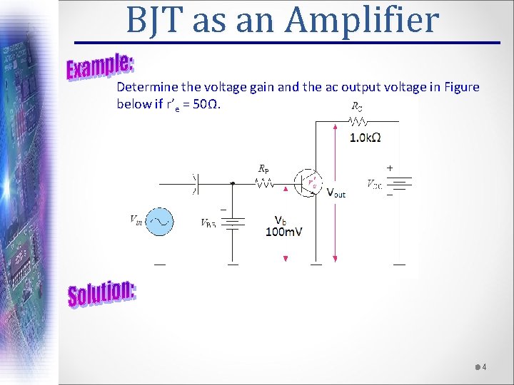
BJT as an Amplifier Determine the voltage gain and the ac output voltage in Figure below if r’e = 50Ω. 4

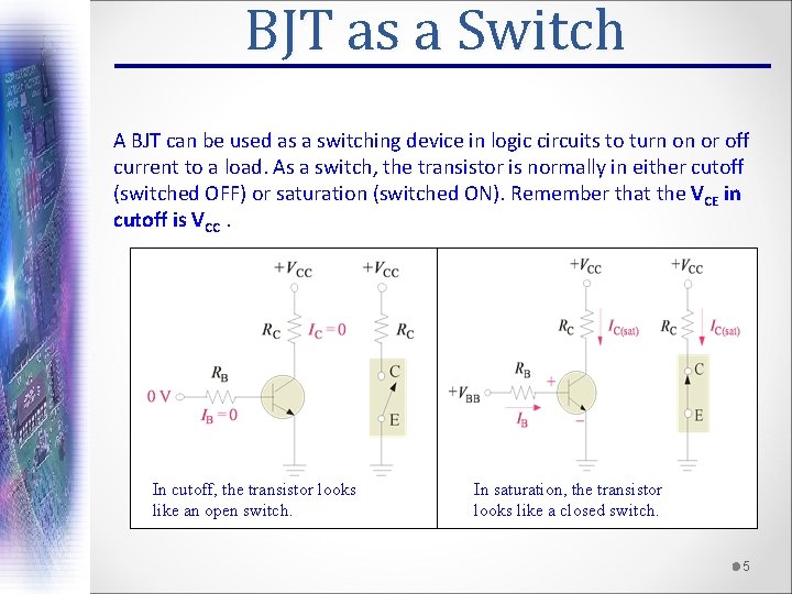
BJT as a Switch A BJT can be used as a switching device in logic circuits to turn on or off current to a load. As a switch, the transistor is normally in either cutoff (switched OFF) or saturation (switched ON). Remember that the VCE in cutoff is VCC. In cutoff, the transistor looks like an open switch. In saturation, the transistor looks like a closed switch. 5

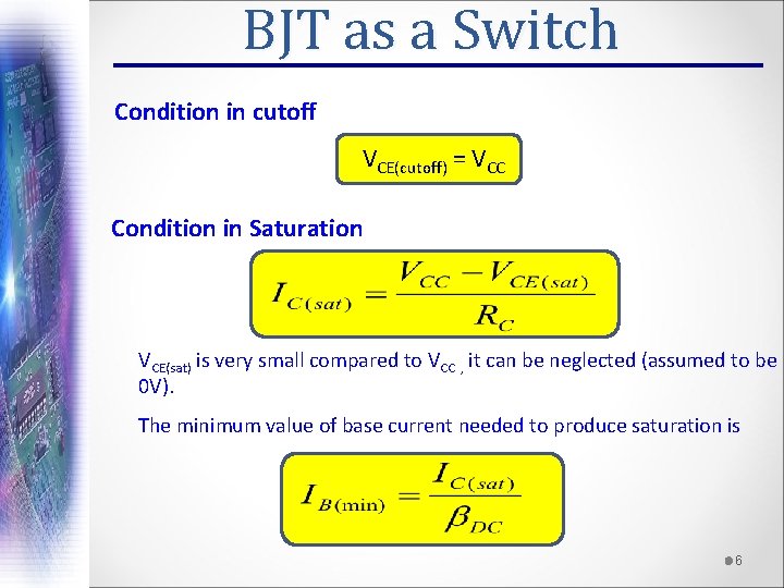
BJT as a Switch Condition in cutoff VCE(cutoff) = VCC Condition in Saturation VCE(sat) is very small compared to VCC , it can be neglected (assumed to be 0 V). The minimum value of base current needed to produce saturation is 6

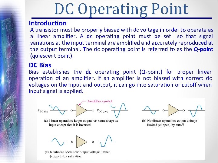
DC Operating Point Introduction A transistor must be properly biased with dc voltage in order to operate as a linear amplifier. A dc operating point must be set so that signal variations at the input terminal are amplified and accurately reproduced at the output terminal. The dc operating point is referred to as the Q-point (quiescent point). DC Bias establishes the dc operating point (Q-point) for proper linear operation of an amplifier. If an amplifier is not biased with correct dc voltages on the input and output, it can go into saturation or cutoff when input signal is applied.

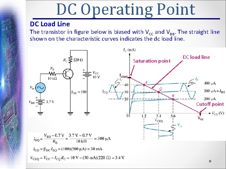
DC Operating Point DC Load Line The transistor in figure below is biased with VCC and VBB. The straight line shown on the characteristic curves indicates the dc load line. Saturation point DC load line IC(sat) Cutoff point VCC

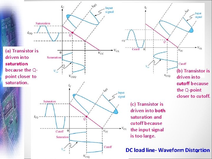
(a) Transistor is driven into saturation because the Qpoint closer to saturation. (b) Transistor is driven into cutoff because the Q-point closer to cutoff. (c) Transistor is driven into both saturation and cutoff because the input signal is too large. DC load line- Waveform Distortion

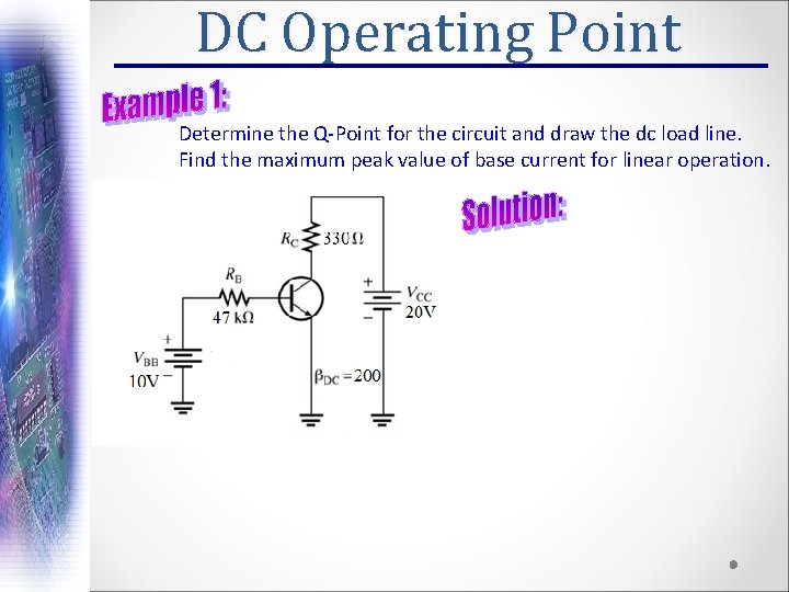
DC Operating Point Determine the Q-Point for the circuit and draw the dc load line. Find the maximum peak value of base current for linear operation.

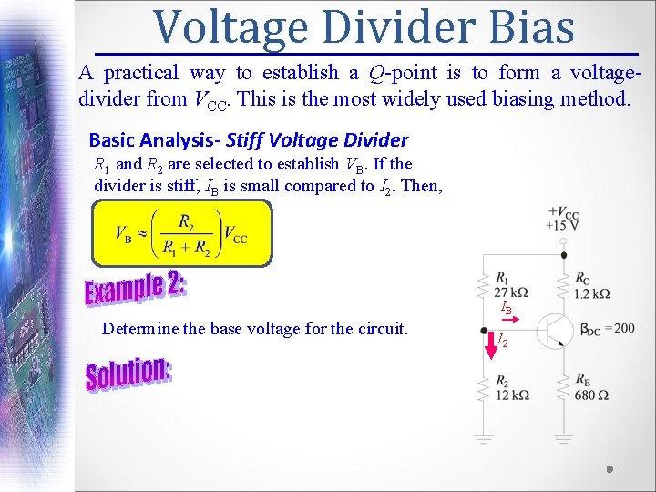
Voltage Divider Bias A practical way to establish a Q-point is to form a voltagedivider from VCC. This is the most widely used biasing method. Basic Analysis- Stiff Voltage Divider R 1 and R 2 are selected to establish VB. If the divider is stiff, IB is small compared to I 2. Then, IB Determine the base voltage for the circuit. I 2

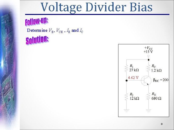
Voltage Divider Bias Determine VE, VCE , IE and IC 4. 62 V

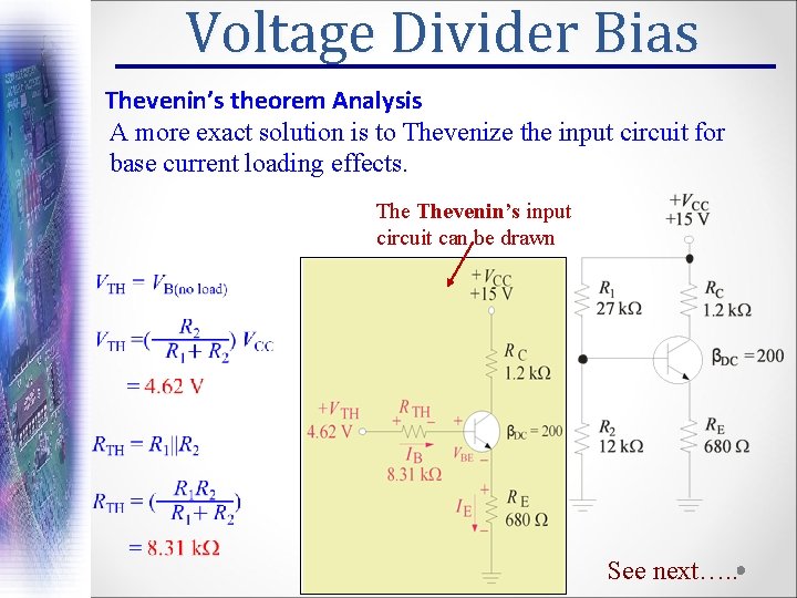
Voltage Divider Bias Thevenin’s theorem Analysis A more exact solution is to Thevenize the input circuit for base current loading effects. Thevenin’s input circuit can be drawn See next…. .

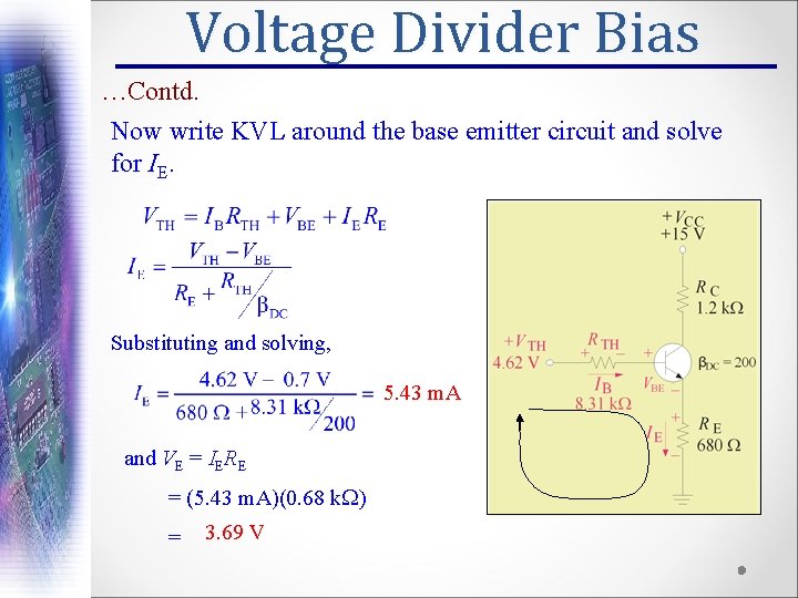
Voltage Divider Bias …Contd. Now write KVL around the base emitter circuit and solve for IE. Substituting and solving, 5. 43 m. A and VE = IERE = (5. 43 m. A)(0. 68 k. W) = 3. 69 V

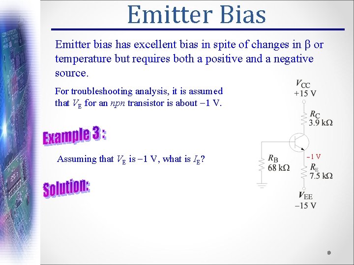
Emitter Bias Emitter bias has excellent bias in spite of changes in β or temperature but requires both a positive and a negative source. For troubleshooting analysis, it is assumed that VE for an npn transistor is about -1 V. Assuming that VE is -1 V, what is IE? -1 V

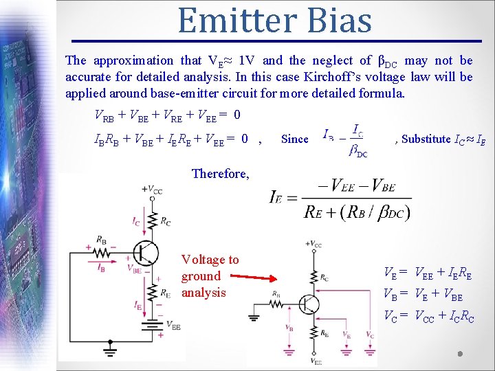
Emitter Bias The approximation that VE≈ 1 V and the neglect of βDC may not be accurate for detailed analysis. In this case Kirchoff’s voltage law will be applied around base-emitter circuit for more detailed formula. VRB + VBE + VRE + VEE = 0 IBRB + VBE + IERE + VEE = 0 , Since , Substitute IC ≈ IE Therefore, Voltage to ground analysis VE = VEE + IERE VB = VE + VBE VC = VCC + ICRC

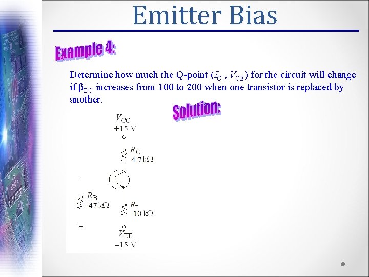
Emitter Bias Determine how much the Q-point (IC , VCE) for the circuit will change if βDC increases from 100 to 200 when one transistor is replaced by another.

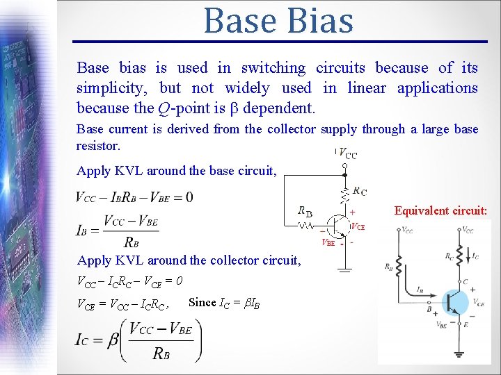
Base Bias Base bias is used in switching circuits because of its simplicity, but not widely used in linear applications because the Q-point is b dependent. Base current is derived from the collector supply through a large base resistor. Apply KVL around the base circuit, Equivalent circuit: Apply KVL around the collector circuit, VCC – ICRC – VCE = 0 VCE = VCC – ICRC , Since IC = IB

Base Bias Determine how much the Q-point (IC , VCE) for the circuit will change if βDC increases from 100 to 200 when one transistor is replaced by another.

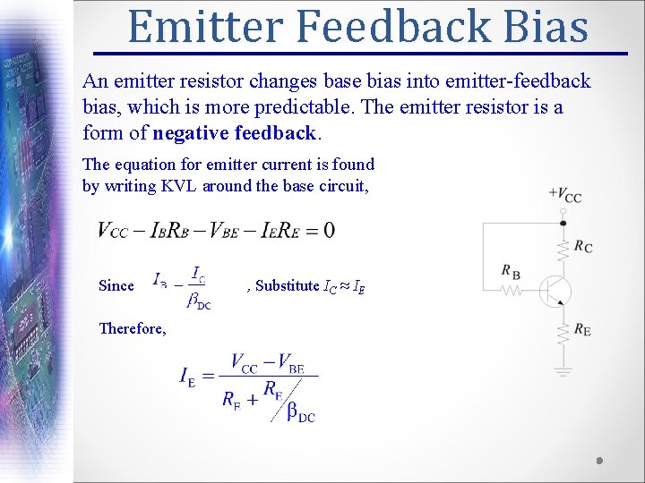
Emitter Feedback Bias An emitter resistor changes base bias into emitter-feedback bias, which is more predictable. The emitter resistor is a form of negative feedback. The equation for emitter current is found by writing KVL around the base circuit, Since Therefore, , Substitute IC ≈ IE

Emitter Feedback Bias The base bias circuit from Example 5 is converted to emitter-feedback bias by the addition of a 1 kΩ emitter resistor. All the other values are the same, and a transistor with a βDC =100 is used. Determine how much the Q-point will change if the first transistor is replaced with one having a βDC =200.

Collector Feedback Bias Collector feedback bias uses another form of negative feedback to increase stability. Instead of returning the base resistor to VCC, it is returned to the collector. The equation for collector current is found by writing KVL around the base circuit. The result is

Collector Feedback Bias Compare IC for the case when b = 100 with the case when b = 300. When b = 100, When b = 300,