Purchase of Wafer AlignerBonder Andrew Loomis April 7
Purchase of Wafer Aligner/Bonder Andrew Loomis April 7, 2000 MIT Lincoln Laboratory
Outline • • • System objectives Alignment options Principles of alignment Bonder functions Available systems Summary MIT Lincoln Laboratory
System Objectives • • • Face to face wafer alignment 0. 25 mm alignment accuracy Hold alignment and bond Robust and void free bond Various bonding options – Anodic – Silicon Fusion – Eutectic – Adhesive MIT Lincoln Laboratory

Alignment Options • • Bottom Side Alignment (BSA) Inter Substrate Alignment (ISA) Top Side Alignment (TSA) Infrared Alignment (IR) MIT Lincoln Laboratory

Principles of Alignment MIT Lincoln Laboratory
Bonder Functions • • Max. bond temperature- 550ºC Max. pressure- 1000 lbs Anodic bonding- 1200 V/ 50 ma Vacuum- 5 E-3 mbar MIT Lincoln Laboratory

Available Systems • Only two companies make wafer align and bond equipment – Karl Suss – Electronic Visions Systems • • Both claim +/- 1 mm accuracy Both companies have similar platforms Barely satisfactory for existing program New system development will be necessary MIT Lincoln Laboratory
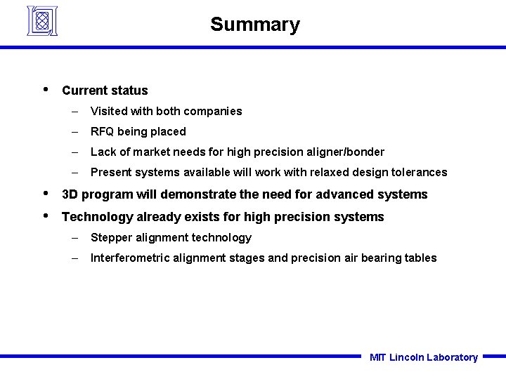
Summary • • • Current status – Visited with both companies – RFQ being placed – Lack of market needs for high precision aligner/bonder – Present systems available will work with relaxed design tolerances 3 D program will demonstrate the need for advanced systems Technology already exists for high precision systems – Stepper alignment technology – Interferometric alignment stages and precision air bearing tables MIT Lincoln Laboratory
- Slides: 8