PulseWidth Modulation PWM Techniques Lecture 25 Instructor Prof

![III. REFERENCES [1] N. Mohan, W. P. Robbin, and T. Undeland, Power Electronics: Converters, III. REFERENCES [1] N. Mohan, W. P. Robbin, and T. Undeland, Power Electronics: Converters,](https://slidetodoc.com/presentation_image_h/14392a557c810534c4ffe95865f9c5d9/image-35.jpg)
- Slides: 35

Pulse-Width Modulation (PWM) Techniques Lecture 25 Instructor: Prof. Ali Keyhani Contact Person: E-mail: keyhani. 1@osu. edu Tel. : 614 -292 -4430 Department of Electrical and Computer Engineering The Ohio State University 1 /35

ORGANIZATION I. Voltage Source Inverter (VSI) A. Six-Step VSI B. Pulse-Width Modulated VSI II. PWM Methods A. Sine PWM B. Hysteresis (Bang-bang) C. Space Vector PWM III. References 2 /35

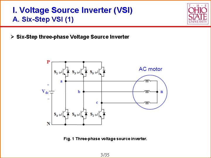
I. Voltage Source Inverter (VSI) A. Six-Step VSI (1) Ø Six-Step three-phase Voltage Source Inverter Fig. 1 Three-phase voltage source inverter. 3 /35

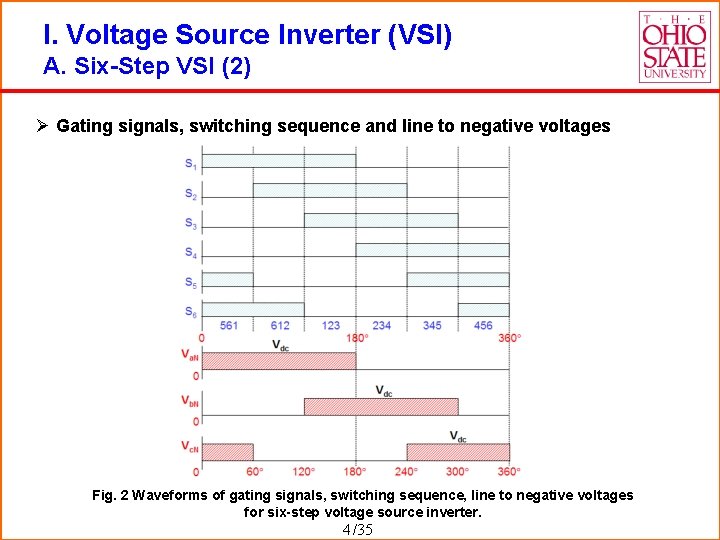
I. Voltage Source Inverter (VSI) A. Six-Step VSI (2) Ø Gating signals, switching sequence and line to negative voltages Fig. 2 Waveforms of gating signals, switching sequence, line to negative voltages for six-step voltage source inverter. 4 /35

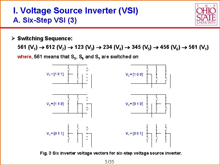
I. Voltage Source Inverter (VSI) A. Six-Step VSI (3) Ø Switching Sequence: 561 (V 1) 612 (V 2) 123 (V 3) 234 (V 4) 345 (V 5) 456 (V 6) 561 (V 1) where, 561 means that S 5, S 6 and S 1 are switched on Fig. 3 Six inverter voltage vectors for six-step voltage source inverter. 5 /35

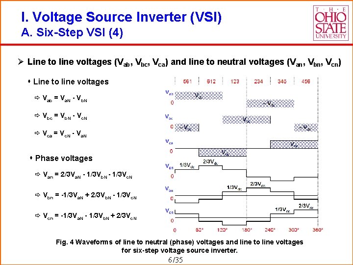
I. Voltage Source Inverter (VSI) A. Six-Step VSI (4) Ø Line to line voltages (Vab, Vbc, Vca) and line to neutral voltages (Van, Vbn, Vcn) s Line to line voltages ð Vab = Va. N - Vb. N ð Vbc = Vb. N - Vc. N ð Vca = Vc. N - Va. N s Phase voltages ð Van = 2/3 Va. N - 1/3 Vb. N - 1/3 Vc. N ð Vbn = -1/3 Va. N + 2/3 Vb. N - 1/3 Vc. N ð Vcn = -1/3 Va. N - 1/3 Vb. N + 2/3 Vc. N Fig. 4 Waveforms of line to neutral (phase) voltages and line to line voltages for six-step voltage source inverter. 6 /35

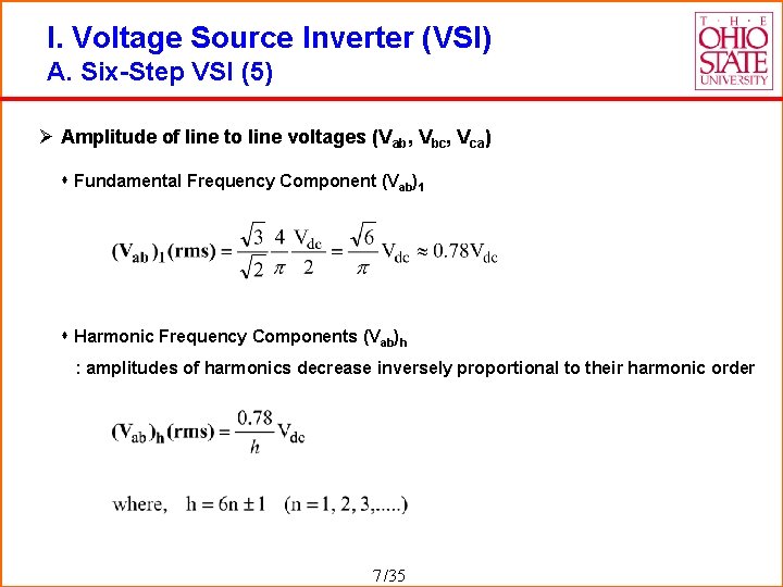
I. Voltage Source Inverter (VSI) A. Six-Step VSI (5) Ø Amplitude of line to line voltages (Vab, Vbc, Vca) s Fundamental Frequency Component (Vab)1 s Harmonic Frequency Components (Vab)h : amplitudes of harmonics decrease inversely proportional to their harmonic order 7 /35

I. Voltage Source Inverter (VSI) A. Six-Step VSI (6) Ø Characteristics of Six-step VSI s It is called “six-step inverter” because of the presence of six “steps” in the line to neutral (phase) voltage waveform s Harmonics of order three and multiples of three are absent from both the line to line and the line to neutral voltages and consequently absent from the currents s Output amplitude in a three-phase inverter can be controlled by only change of DC-link voltage (Vdc) 8 /35

I. Voltage Source Inverter (VSI) B. Pulse-Width Modulated VSI (1) Ø Objective of PWM s Control of inverter output voltage s Reduction of harmonics Ø Disadvantages of PWM s Increase of switching losses due to high PWM frequency s Reduction of available voltage s EMI problems due to high-order harmonics 9 /35

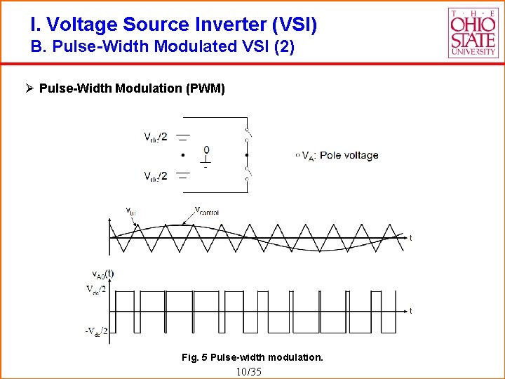
I. Voltage Source Inverter (VSI) B. Pulse-Width Modulated VSI (2) Ø Pulse-Width Modulation (PWM) Fig. 5 Pulse-width modulation. 10 /35

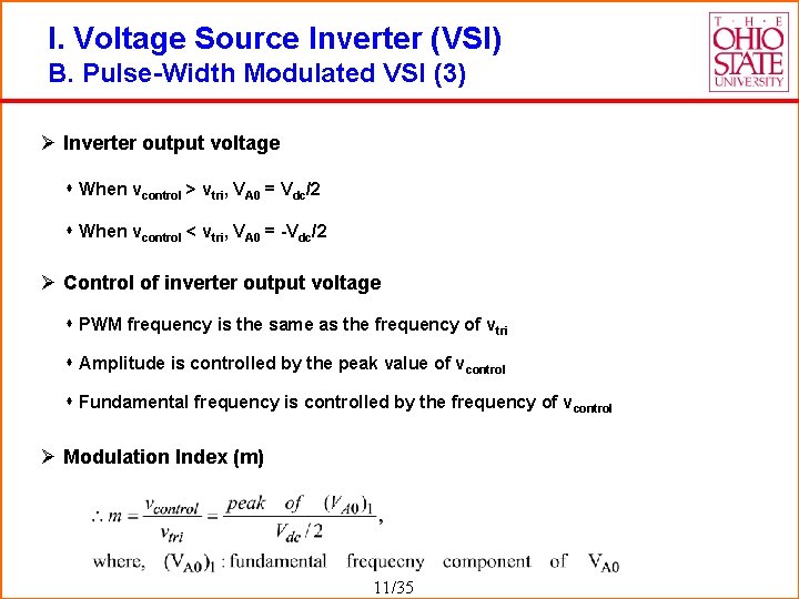
I. Voltage Source Inverter (VSI) B. Pulse-Width Modulated VSI (3) Ø Inverter output voltage s When vcontrol > vtri, VA 0 = Vdc/2 s When vcontrol < vtri, VA 0 = -Vdc/2 Ø Control of inverter output voltage s PWM frequency is the same as the frequency of vtri s Amplitude is controlled by the peak value of vcontrol s Fundamental frequency is controlled by the frequency of vcontrol Ø Modulation Index (m) 11 /35

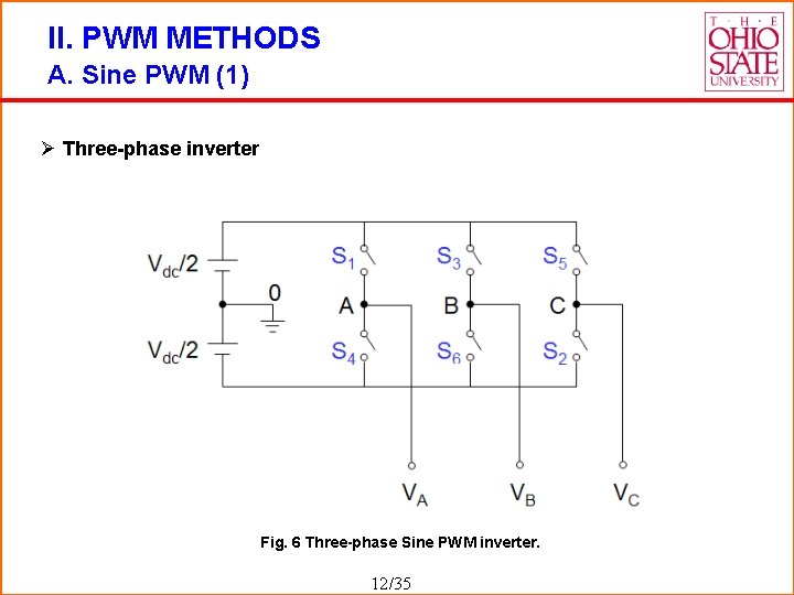
II. PWM METHODS A. Sine PWM (1) Ø Three-phase inverter Fig. 6 Three-phase Sine PWM inverter. 12 /35

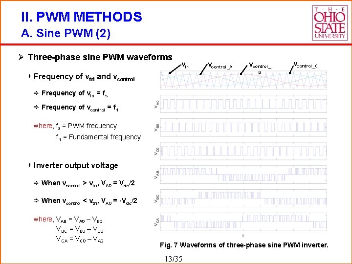
II. PWM METHODS A. Sine PWM (2) Ø Three-phase sine PWM waveforms vtri vcontrol_A vcontrol_C B s Frequency of vtri and vcontrol ð Frequency of vtri = fs ð Frequency of vcontrol = f 1 where, fs = PWM frequency f 1 = Fundamental frequency s Inverter output voltage ð When vcontrol > vtri, VA 0 = Vdc/2 ð When vcontrol < vtri, VA 0 = -Vdc/2 where, VAB = VA 0 – VB 0 VBC = VB 0 – VC 0 VCA = VC 0 – VA 0 Fig. 7 Waveforms of three-phase sine PWM inverter. 13 /35

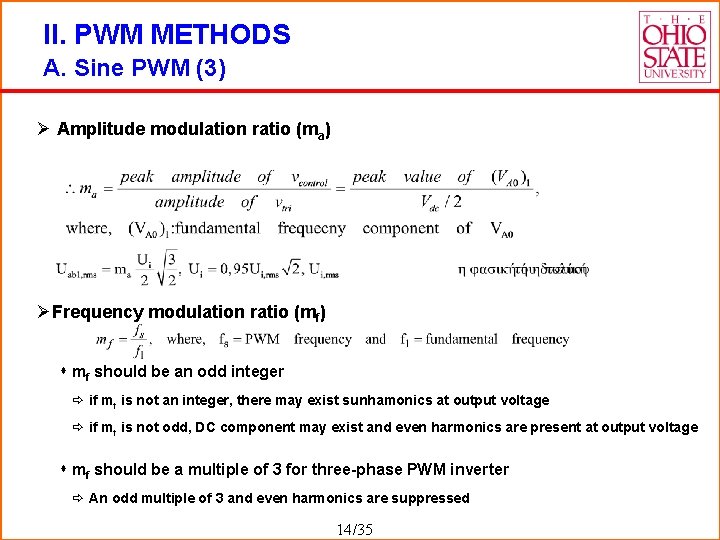
II. PWM METHODS A. Sine PWM (3) Ø Amplitude modulation ratio (ma) ØFrequency modulation ratio (mf) s mf should be an odd integer ð if mf is not an integer, there may exist sunhamonics at output voltage ð if mf is not odd, DC component may exist and even harmonics are present at output voltage s mf should be a multiple of 3 for three-phase PWM inverter ð An odd multiple of 3 and even harmonics are suppressed 14 /35

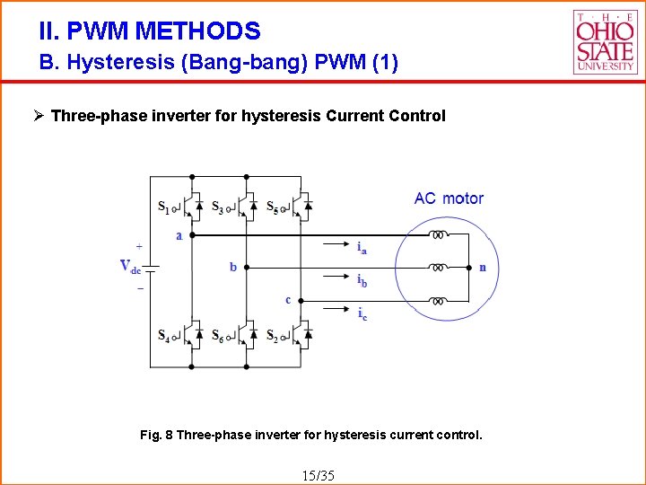
II. PWM METHODS B. Hysteresis (Bang-bang) PWM (1) Ø Three-phase inverter for hysteresis Current Control Fig. 8 Three-phase inverter for hysteresis current control. 15 /35

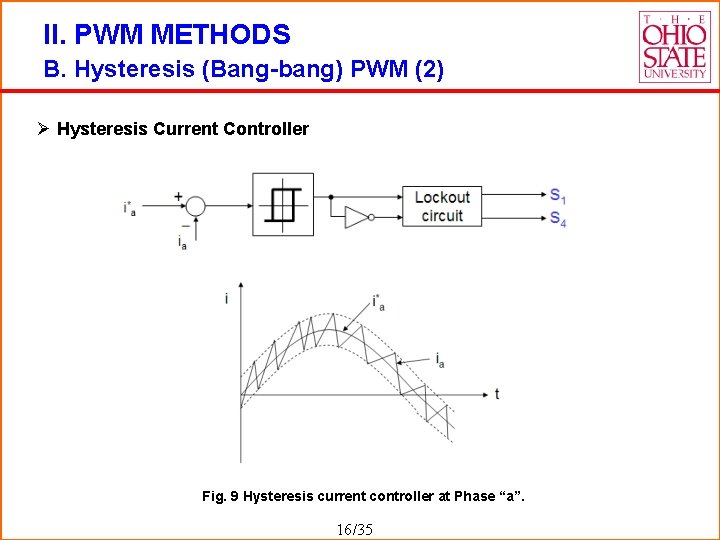
II. PWM METHODS B. Hysteresis (Bang-bang) PWM (2) Ø Hysteresis Current Controller Fig. 9 Hysteresis current controller at Phase “a”. 16 /35

II. PWM METHODS B. Hysteresis (Bang-bang) PWM (3) Ø Characteristics of hysteresis Current Control s Advantages ð Excellent dynamic response ð Low cost and easy implementation s Drawbacks ð Large current ripple in steady-state ð Variation of switching frequency ð No intercommunication between each hysterisis controller of three phases and hence no strategy to generate zero-voltage vectors. As a result, the switching frequency increases at lower modulation index and the signal will leave the hysteresis band whenever the zero vector is turned on. ð The modulation process generates subharmonic components 17 /35

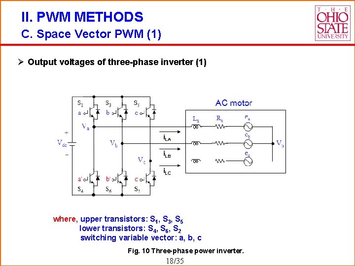
II. PWM METHODS C. Space Vector PWM (1) Ø Output voltages of three-phase inverter (1) where, upper transistors: S 1, S 3, S 5 lower transistors: S 4, S 6, S 2 switching variable vector: a, b, c Fig. 10 Three-phase power inverter. 18 /35

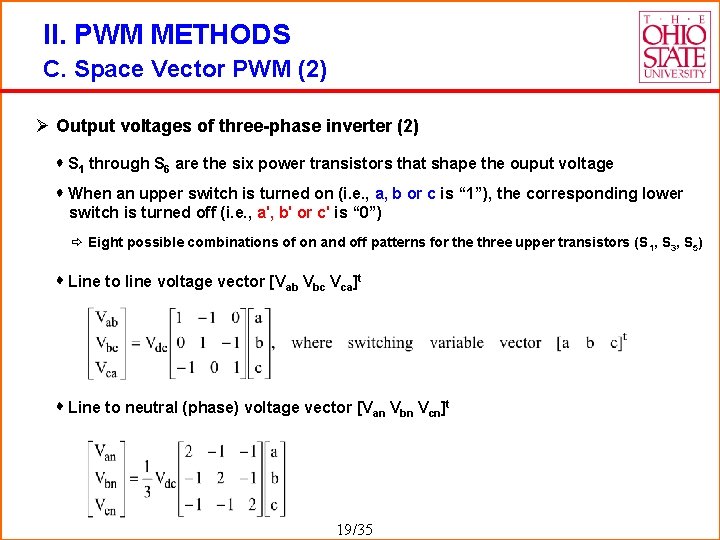
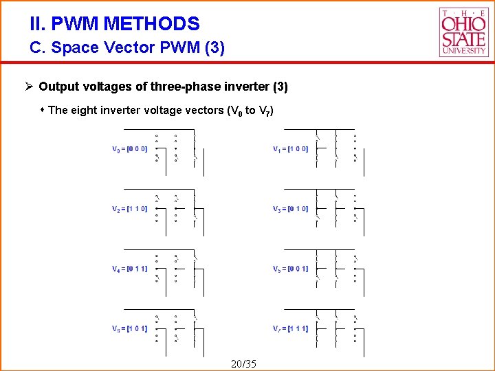
II. PWM METHODS C. Space Vector PWM (2) Ø Output voltages of three-phase inverter (2) S 1 through S 6 are the six power transistors that shape the ouput voltage When an upper switch is turned on (i. e. , a, b or c is “ 1”), the corresponding lower switch is turned off (i. e. , a', b' or c' is “ 0”) ð Eight possible combinations of on and off patterns for the three upper transistors (S 1, S 3, S 5) Line to line voltage vector [Vab Vbc Vca]t Line to neutral (phase) voltage vector [Van Vbn Vcn]t 19 /35

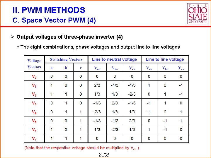
II. PWM METHODS C. Space Vector PWM (3) Ø Output voltages of three-phase inverter (3) s The eight inverter voltage vectors (V 0 to V 7) 20 /35

II. PWM METHODS C. Space Vector PWM (4) Ø Output voltages of three-phase inverter (4) s The eight combinations, phase voltages and output line to line voltages 21 /35

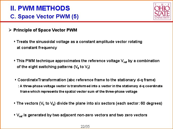
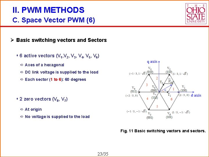
II. PWM METHODS C. Space Vector PWM (5) Ø Principle of Space Vector PWM s Treats the sinusoidal voltage as a constant amplitude vector rotating at constant frequency s This PWM technique approximates the reference voltage Vref by a combination of the eight switching patterns (V 0 to V 7) s Coordinate. Transformation (abc reference frame to the stationary d-q frame) : A three-phase voltage vector is transformed into a vector in the stationary d-q coordinate frame which represents the spatial vector sum of the three-phase voltage s The vectors (V 1 to V 6) divide the plane into six sectors (each sector: 60 degrees) s Vref is generated by two adjacent non-zero vectors and two zero vectors 22 /35

II. PWM METHODS C. Space Vector PWM (6) Ø Basic switching vectors and Sectors s 6 active vectors (V 1, V 2, V 3, V 4, V 5, V 6) ð Axes of a hexagonal ð DC link voltage is supplied to the load ð Each sector (1 to 6): 60 degrees s 2 zero vectors (V 0, V 7) ð At origin ð No voltage is supplied to the load Fig. 11 Basic switching vectors and sectors. 23 /35

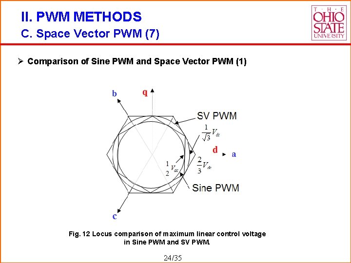
II. PWM METHODS C. Space Vector PWM (7) Ø Comparison of Sine PWM and Space Vector PWM (1) Fig. 12 Locus comparison of maximum linear control voltage in Sine PWM and SV PWM. 24 /35

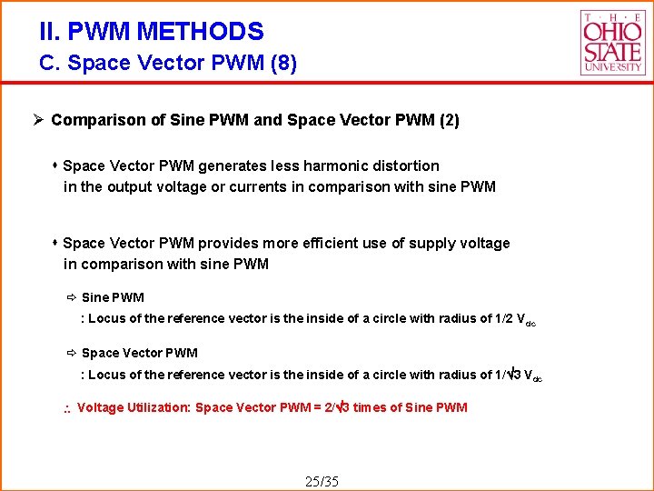
II. PWM METHODS C. Space Vector PWM (8) Ø Comparison of Sine PWM and Space Vector PWM (2) s Space Vector PWM generates less harmonic distortion in the output voltage or currents in comparison with sine PWM s Space Vector PWM provides more efficient use of supply voltage in comparison with sine PWM ð Sine PWM : Locus of the reference vector is the inside of a circle with radius of 1/2 V dc ð Space Vector PWM : Locus of the reference vector is the inside of a circle with radius of 1/ 3 Vdc Voltage Utilization: Space Vector PWM = 2/ 3 times of Sine PWM 25 /35

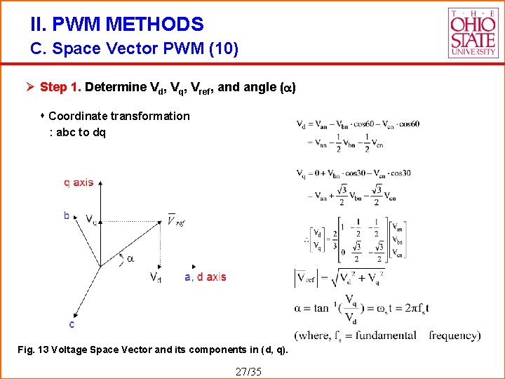
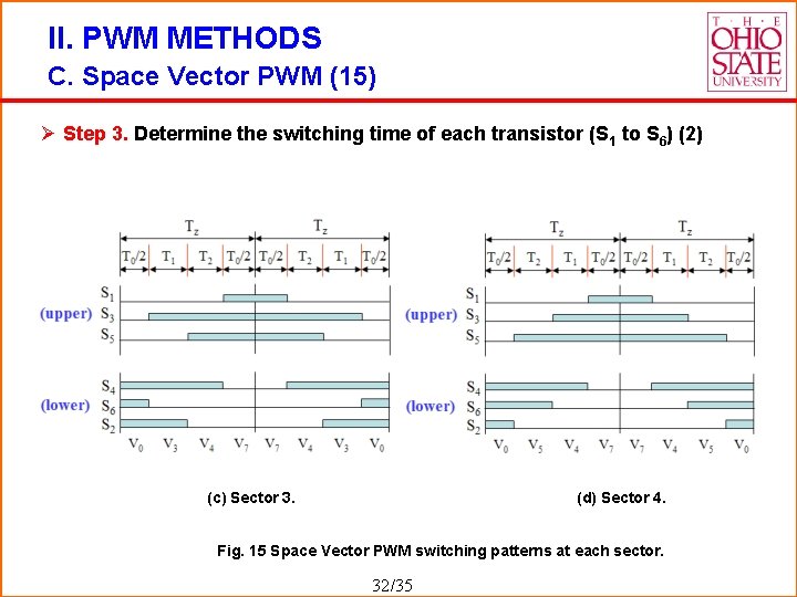
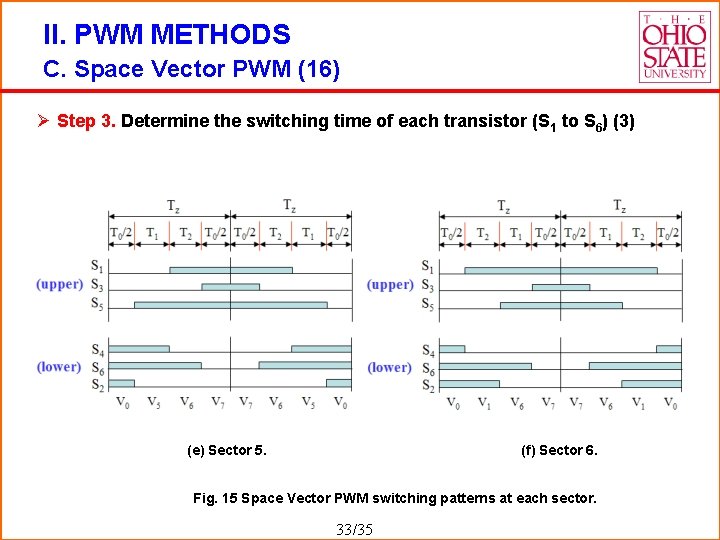
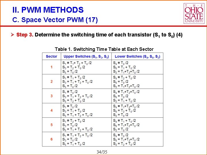
II. PWM METHODS C. Space Vector PWM (9) Ø Realization of Space Vector PWM s Step 1. Determine Vd, Vq, Vref, and angle ( ) s Step 2. Determine time duration T 1, T 2, T 0 s Step 3. Determine the switching time of each transistor (S 1 to S 6) 26 /35

II. PWM METHODS C. Space Vector PWM (10) Ø Step 1. Determine Vd, Vq, Vref, and angle ( ) s Coordinate transformation : abc to dq Fig. 13 Voltage Space Vector and its components in (d, q). 27 /35

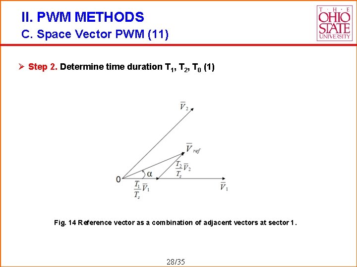
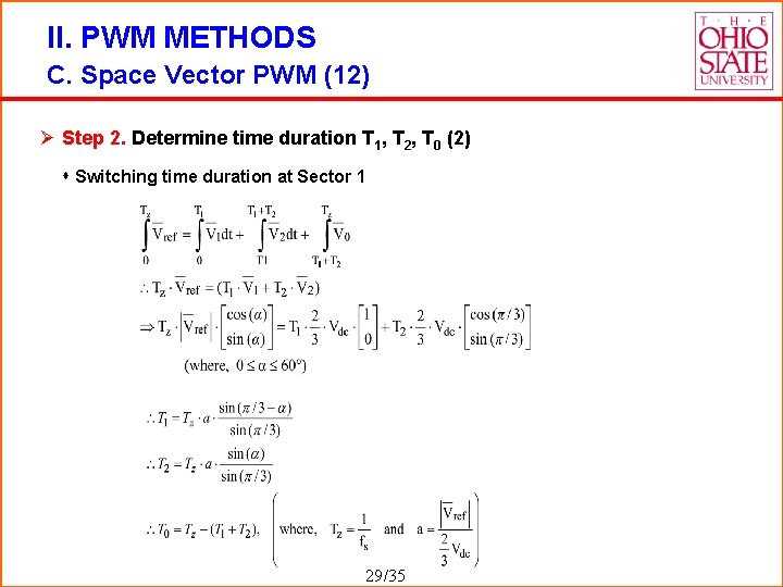
II. PWM METHODS C. Space Vector PWM (11) Ø Step 2. Determine time duration T 1, T 2, T 0 (1) Fig. 14 Reference vector as a combination of adjacent vectors at sector 1. 28 /35

II. PWM METHODS C. Space Vector PWM (12) Ø Step 2. Determine time duration T 1, T 2, T 0 (2) s Switching time duration at Sector 1 29 /35

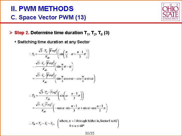
II. PWM METHODS C. Space Vector PWM (13) Ø Step 2. Determine time duration T 1, T 2, T 0 (3) s Switching time duration at any Sector 30 /35

II. PWM METHODS C. Space Vector PWM (14) Ø Step 3. Determine the switching time of each transistor (S 1 to S 6) (1) (a) Sector 1. (b) Sector 2. Fig. 15 Space Vector PWM switching patterns at each sector. 31 /35

II. PWM METHODS C. Space Vector PWM (15) Ø Step 3. Determine the switching time of each transistor (S 1 to S 6) (2) (c) Sector 3. (d) Sector 4. Fig. 15 Space Vector PWM switching patterns at each sector. 32 /35

II. PWM METHODS C. Space Vector PWM (16) Ø Step 3. Determine the switching time of each transistor (S 1 to S 6) (3) (e) Sector 5. (f) Sector 6. Fig. 15 Space Vector PWM switching patterns at each sector. 33 /35

II. PWM METHODS C. Space Vector PWM (17) Ø Step 3. Determine the switching time of each transistor (S 1 to S 6) (4) Table 1. Switching Time Table at Each Sector 34 /35
![III REFERENCES 1 N Mohan W P Robbin and T Undeland Power Electronics Converters III. REFERENCES [1] N. Mohan, W. P. Robbin, and T. Undeland, Power Electronics: Converters,](https://slidetodoc.com/presentation_image_h/14392a557c810534c4ffe95865f9c5d9/image-35.jpg)
III. REFERENCES [1] N. Mohan, W. P. Robbin, and T. Undeland, Power Electronics: Converters, Applications, and Design, 2 nd ed. New York: Wiley, 1995. [2] B. K. Bose, Power Electronics and Variable Frequency Drives: Technology and Applications. IEEE Press, 1997. [3] H. W. van der Broeck, H. -C. Skudelny, and G. V. Stanke, “Analysis and realization of a pulsewidth modulator based on voltage space vectors, ” IEEE Transactions on Industry Applications, vol. 24, pp. 142 -150, 1988. 35 /35