PSPICE Simulation Program with Integrated Circuit Emphasis CH




- Slides: 56

PSPICE计算机仿真 Simulation Program with Integrated Circuit Emphasis

CH 12 FREQUENCY RESPONSE 频率响应

12. 1 specifying frequency variation and number

n Sinusoidal n Linear, Logarithmic n Decade, octave

12. 2 frequency response output n Rectangular, polar, decibel

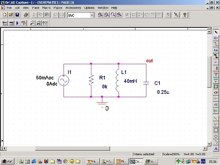
n Example 18 illustrates how to analyze the frequency response of a parallel RLC circuit with PSpice.

Fig. 104 ddb

Example 18 n n n a) The current source in the circuit shown in Fig. 104 is 50 cosωt m. A. Use Probe to plot Vo versus f from 1000 to 2000 Hz in increments of 10 Hz on a linear frequency scale. b) From the Probe plot, estimate the resonant frequency, the bandwidth, and the quality factor of the circuit. c) Compare the results obtained in b) with an analytic solution for f 0, β, and Q.

Solution a & b

Fig. 105 sch

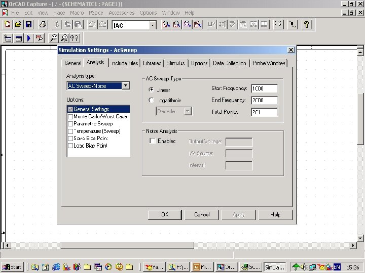
Fig. 106 setting

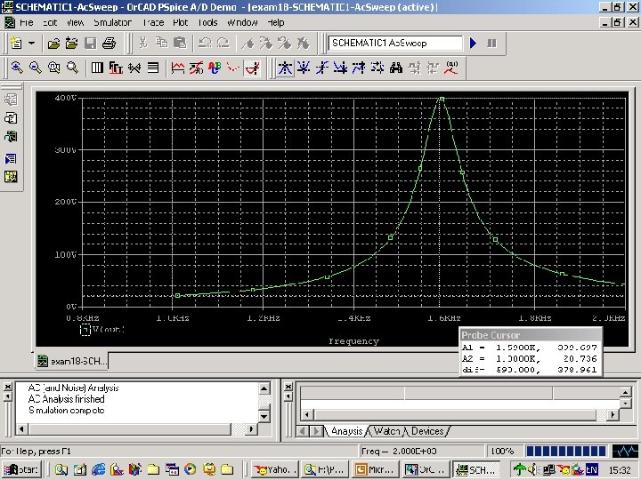
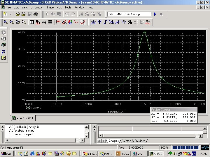
n n Using the Probe Cursor, we note that the peak amplitude(峰值振幅) of about 400 V occurs at a frequency of 1590 Hz in Fig. 107 a. Thus we estimate the resonant frequency(衰减频率) at 1590 Hz.

Fig. 107 a probe

n n n To estimate the bandwidth, we use both cursors to find the frequencies where Vo=399. 697/1. 414=282. 67 V. The closest values are 281. 992 at 1552 Hz and 1632. 1 Hz. (Fig. 107 b) Thus we estimate the bandwidth to be 1632. 1 - 1552, or about 80 Hz.

Fig. 107 b

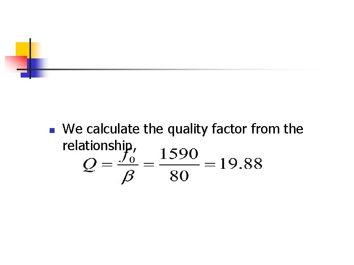
n We calculate the quality factor from the relationship,

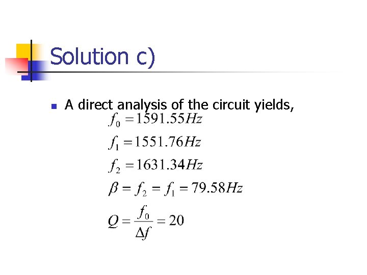
Solution c) n A direct analysis of the circuit yields,

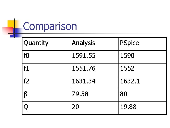
Comparison Quantity Analysis PSpice f 0 1591. 55 1590 f 1 1551. 76 1552 f 2 1631. 34 1632. 1 β 79. 58 80 Q 20 19. 88

Example 19

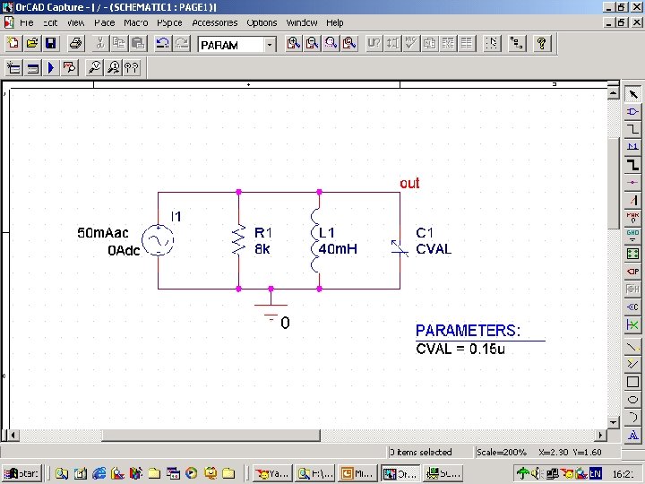
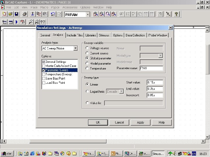
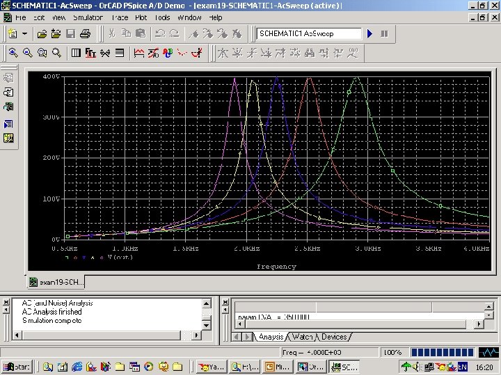
Example 19 n n n Modify the PSpice schematic for Example 18 to step the capacitor values from 0. 15 μF through 0. 35 μF. Then use Probe to display the frequency response characteristics for all values of capacitance. Comment on the effect of the changing capacitance.

Solution

Fig. 108 sch

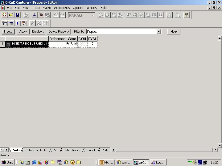
Fig. 108 a param property

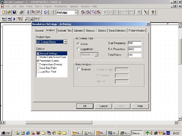
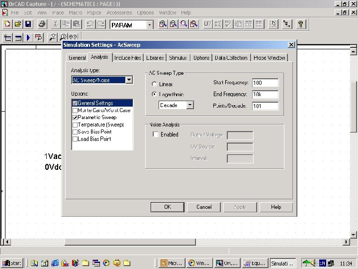
Fig. 108 b setting

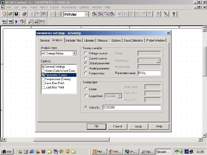
Fig. 108 c Param_setting

Fig. 109 Probe

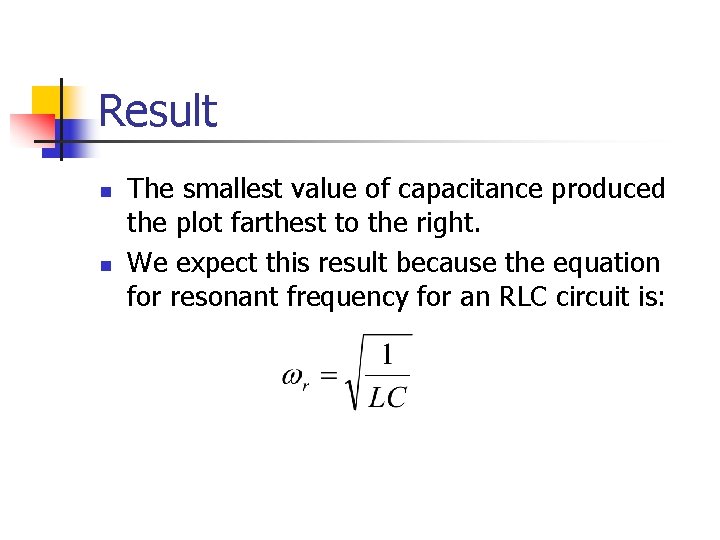
Result n n The smallest value of capacitance produced the plot farthest to the right. We expect this result because the equation for resonant frequency for an RLC circuit is:

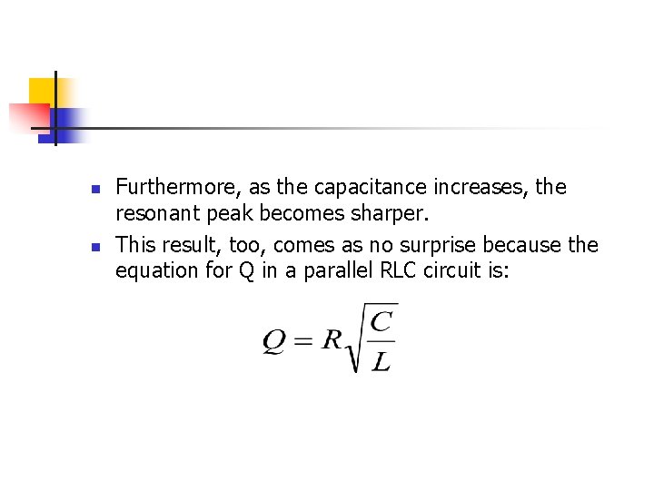
n n Furthermore, as the capacitance increases, the resonant peak becomes sharper. This result, too, comes as no surprise because the equation for Q in a parallel RLC circuit is:

12. 3 Bode plots with probe

Fig. 110 ddb

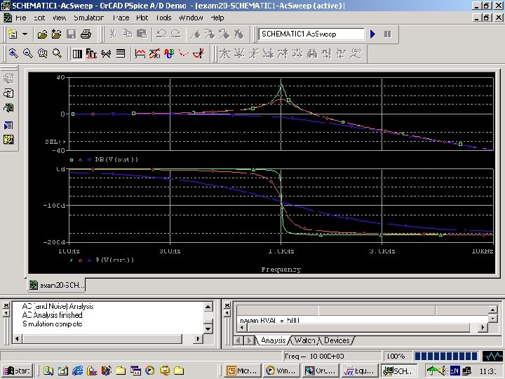
n Example 20 compares the exact d. B voltage magnitude versus log frequency and phase angle versus log frequency plots to the Bode straight-line approximation using Probe.

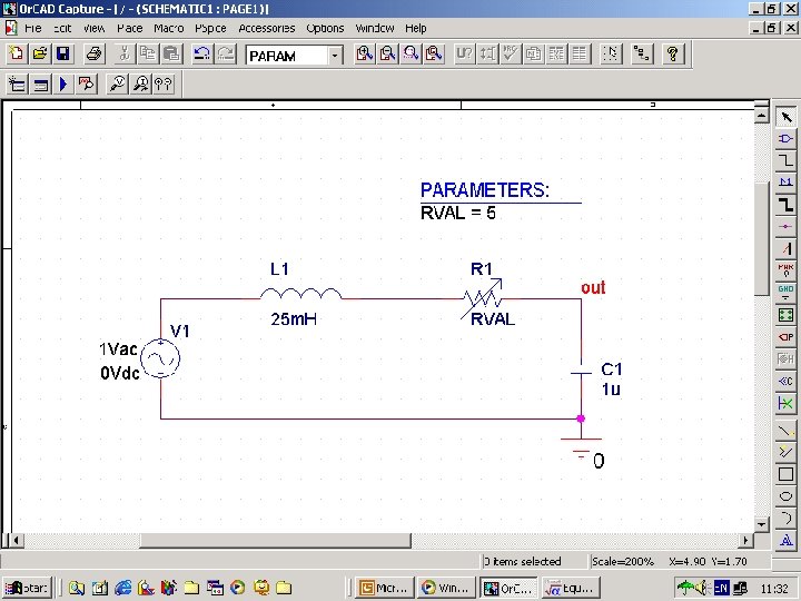
Example 20 n n n Construct a PSpice schematic and associated analysis to generate the frequency response of the circuit shown in Fig. 110 for three different values of resistance: 5 Ω, 50 Ω, and 500 Ω. Then use Probe to plot the output voltage magnitude in d. B and output voltage phase angle versus log frequency. Finally, use the Label tool in Probe to overlay a straight-line Bode approximation plot and comment.

Fig. 111 sch

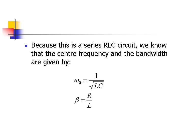
n Because this is a series RLC circuit, we know that the centre frequency and the bandwidth are given by:

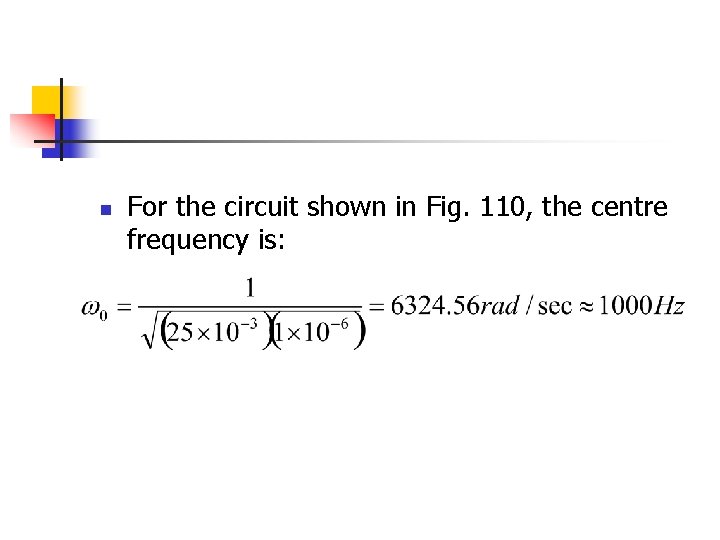
n For the circuit shown in Fig. 110, the centre frequency is:

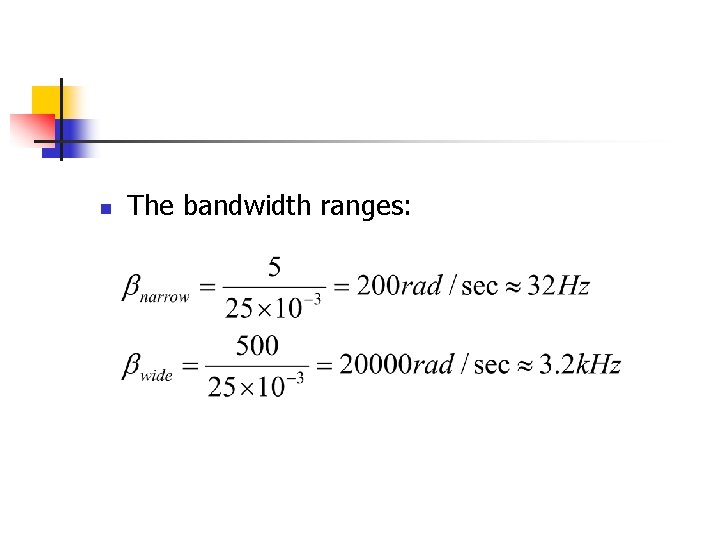
n The bandwidth ranges:

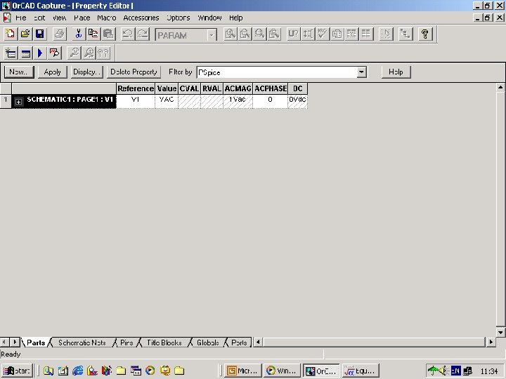
Fig. 111 a param_property

Fig. 111 b vac_property

Fig. 111 c setting 1

Fig. 111 d setting 2

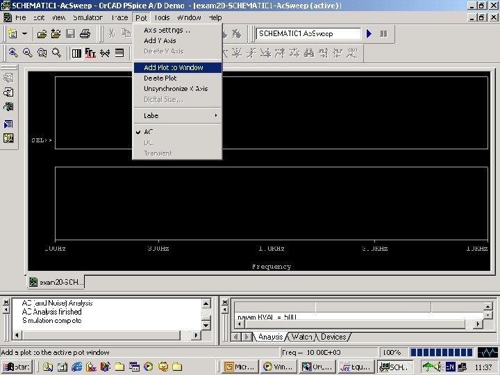
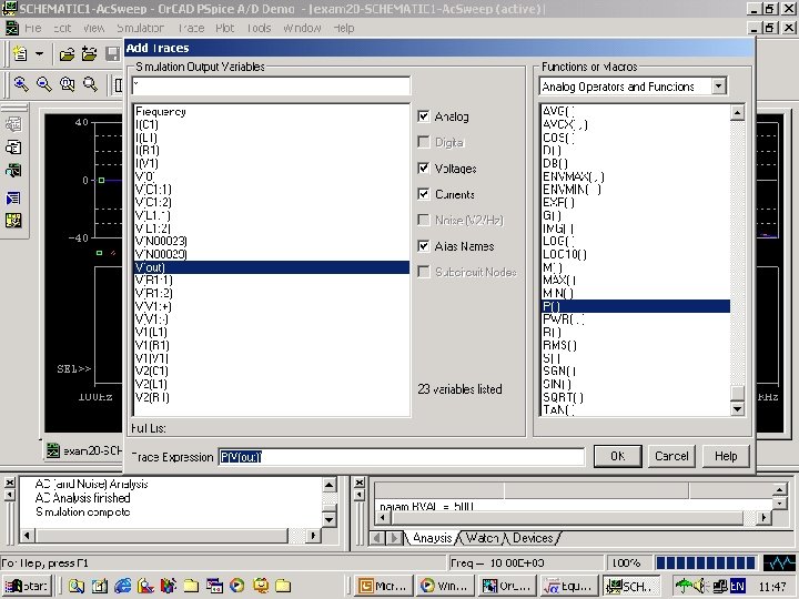
Fig. 112 a Plot/Add plot to window


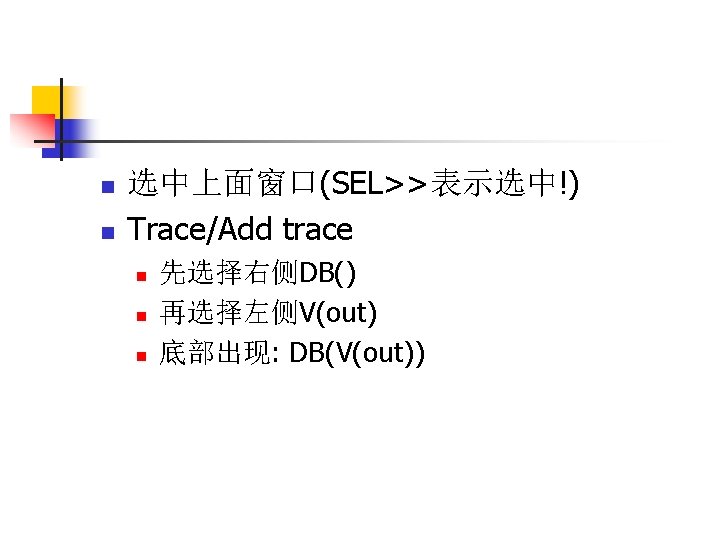
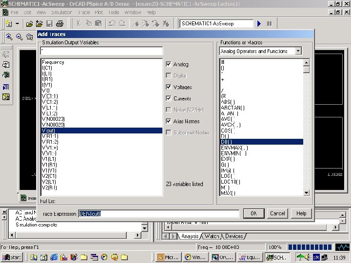
Fig. 112 b select DB(V(out))


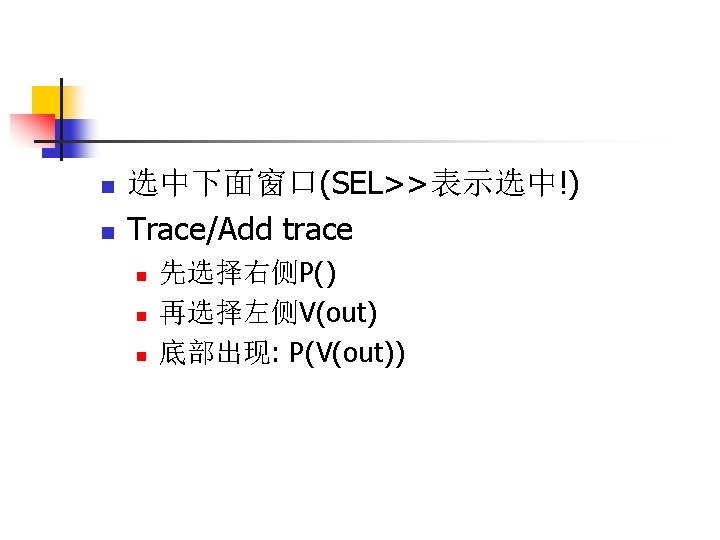
Fig. 112 c select P(V(out))

Fig. 112 probe

12. 4 Filter design

n Example 21 demonstrates the use of PSpice and Probe in verifying the behavior of a high-Q bandpass filter.

Fig. 113 ddb

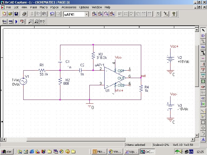
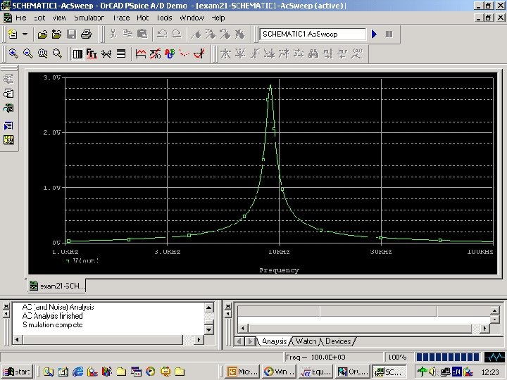
Example 21 n n n The circuit in Fig. 113 is an active high-Q bandpass filter. Using 1 n. F capacitors and an ideal op amp, design values for the three resistors to yield a centre frequency of 10 KHz, a quality factor of 10, and a passband gain of 3. Use Probe to verify that the resistor values you compute produce a filter that satisfies the three frequency response specifications.

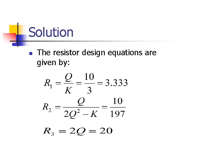
Solution n The resistor design equations are given by:

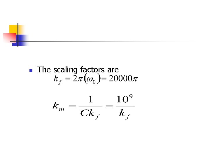
n The scaling factors are

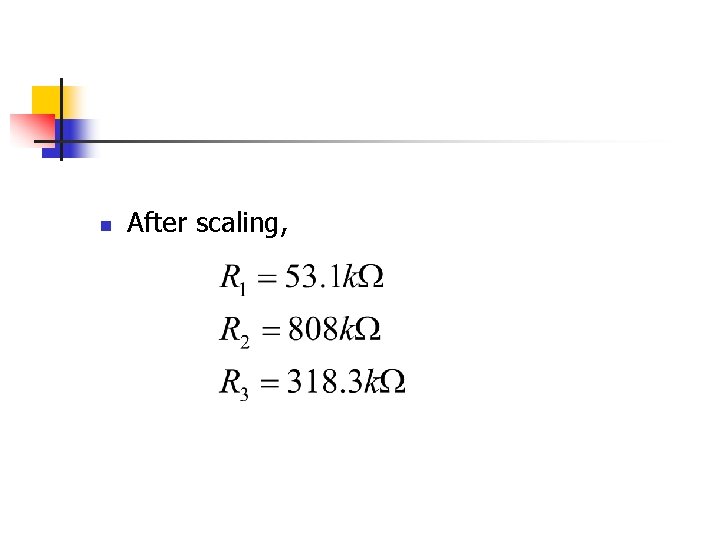
n After scaling,

Fig. 114 Sch

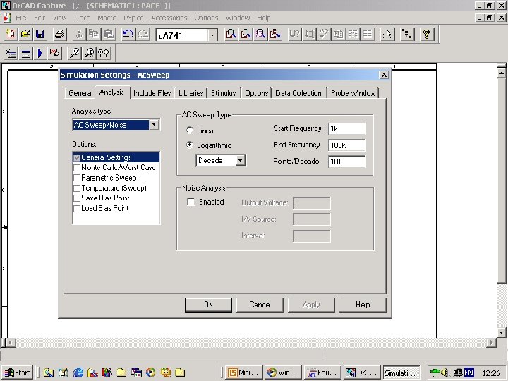
Fig. 114 a setting

Fig. 115 probe