PSo C Designer Module 1 Introduction to PSo

![Project Implementation Pup PSo. C 16 -bit PWM ÷ 65535 ÷ 16 P 2[0] Project Implementation Pup PSo. C 16 -bit PWM ÷ 65535 ÷ 16 P 2[0]](https://slidetodoc.com/presentation_image/57e301a8ccd74541a05eb2ebc452c8fd/image-37.jpg)
- Slides: 76

PSo. C Designer Module 1: Introduction to PSo. C

Module Outline Section 1: Introduction to PSo. C Section 2: PSo. C Designer™ IDE Software Section 3: Hands-On Example Project 2

PSo. C An Introduction

What is a PSo. C Mixed Signal Device? P rogrammable S ystem on C hip PSo. C combines: • the familiarity of a microcontroller • the configurability of an CPLD • the capabilities of an Mixed – Signal Array 4

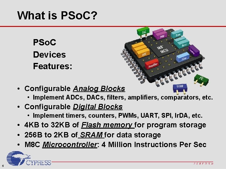
What is PSo. C? PSo. C Devices Features: • Configurable Analog Blocks • Implement ADCs, DACs, filters, amplifiers, comparators, etc. • Configurable Digital Blocks • Implement timers, counters, PWMs, UART, SPI, Ir. DA, etc. • 4 KB to 32 KB of Flash memory for program storage • 256 B to 2 KB of SRAM for data storage • M 8 C Microcontroller: 4 Million Instructions Per Sec 5

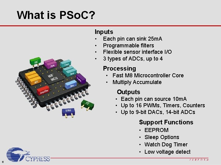
What is PSo. C? Inputs • • Each pin can sink 25 m. A Programmable filters Flexible sensor interface I/O 3 types of ADCs, up to 4 Processing • Fast M 8 Microcontroller Core • Multiply Accumulate Outputs • Each pin can source 10 m. A • Up to 16 PWMs, Timers, Counters • Up to 9 -bit DACs, 14 -bit ADCs Support Functions • • 6 EEPROM Sleep Options Watch Dog Timer Low voltage detect

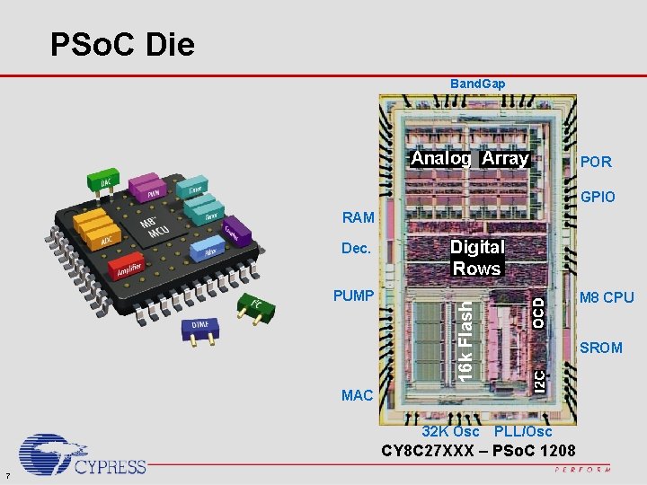
PSo. C Die Band. Gap POR GPIO RAM Dec. M 8 CPU 16 k Flash PUMP SROM MAC 32 K Osc PLL/Osc CY 8 C 27 XXX – PSo. C 1208 7

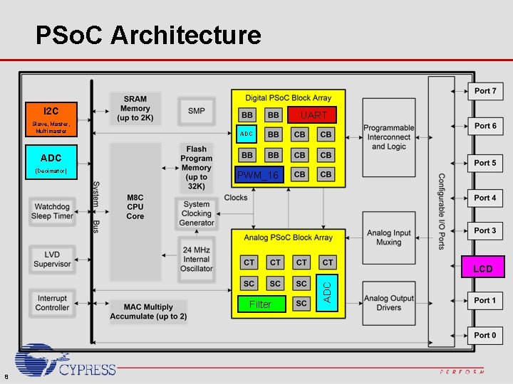
PSo. C Architecture I 2 C Slave, Master, Multimaster UART ADC (Decimator) PWM_16 Filter 8 ADC LCD

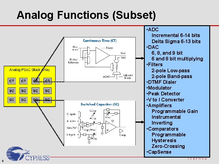
Analog Functions (Subset) • ADC Incremental 6 -14 bits Delta Sigma 6 -13 bits • DAC 6, 8, and 9 bit 6 and 8 bit multiplying • Filters 2 -pole Low-pass 2 -pole Band-pass • DTMF Dialer • Modulator • Peak Detector • V to I Converter • Amplifiers Programmable Gain Instrumental Inverting • Comparators Programmable Hysteresis Zero-Crossing • Cap. Sense 9

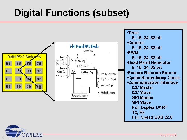
Digital Functions (subset) • Timer 8, 16, 24, 32 bit • Counter 8, 16, 24, 32 bit • PWM 8, 16, 24, 32 bit • Dead Band Generator 8, 16, 24, 32 bit • Pseudo Random Source • Cyclic Redundancy Check • Communication Interface I 2 C Master I 2 C Slave SPI Master SPI Slave Full Duplex UART Tx, Rx Full Speed USB v 2. 0 10

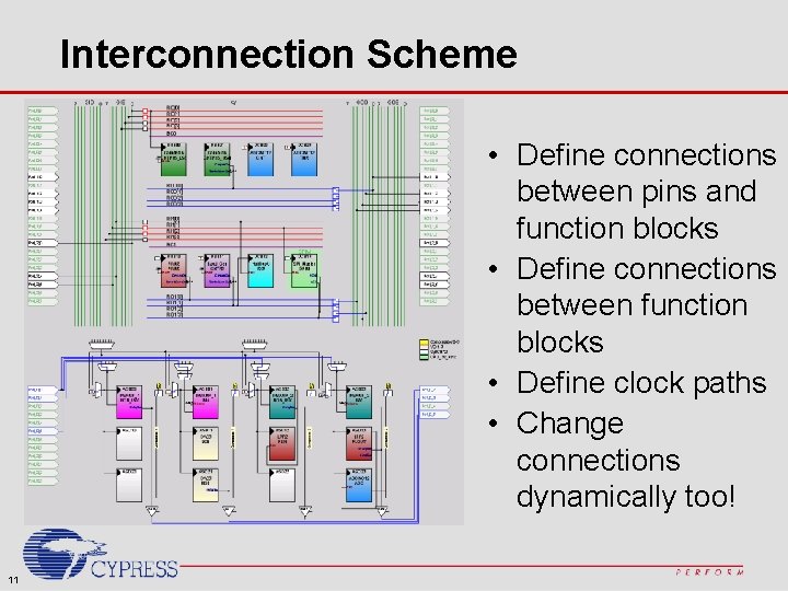
Interconnection Scheme • Define connections between pins and function blocks • Define connections between function blocks • Define clock paths • Change connections dynamically too! 11

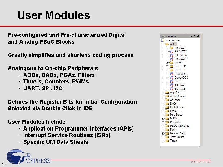
User Modules Pre-configured and Pre-characterized Digital and Analog PSo. C Blocks Greatly simplifies and shortens coding process Analogous to On-chip Peripherals • ADCs, DACs, PGAs, Filters • Timers, Counters, PWMs • UART, SPI, I 2 C Defines the Register Bits for Initial Configuration Selected via Double Click in IDE User Modules Include • Application Programmer Interfaces (APIs) • Interrupt Service Routines (ISRs) • Specific UM Data Sheets 12

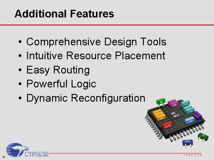
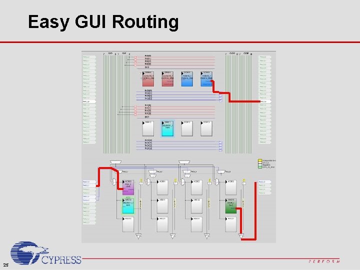
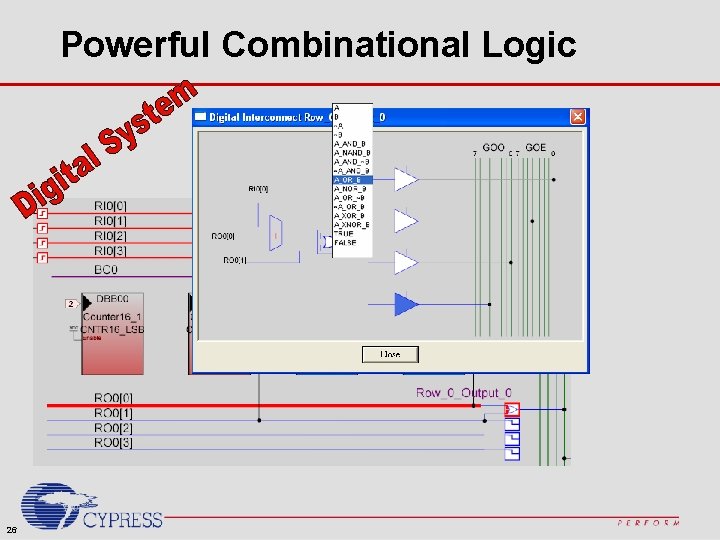
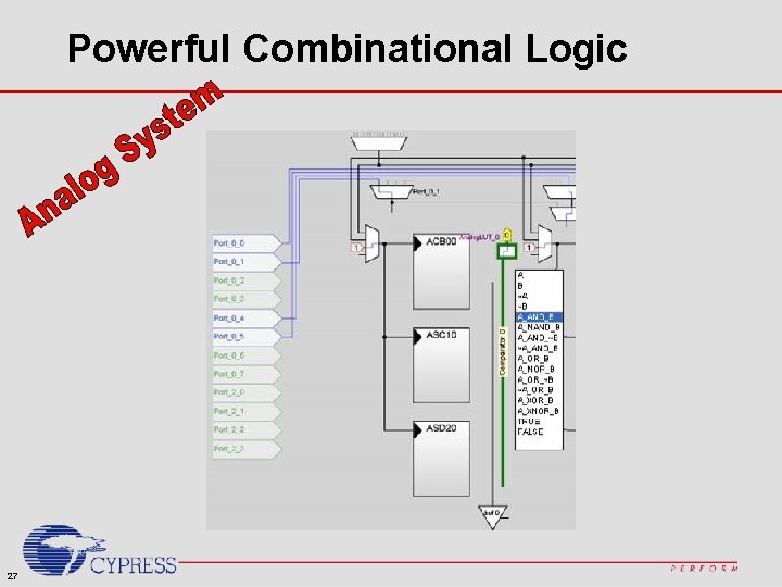
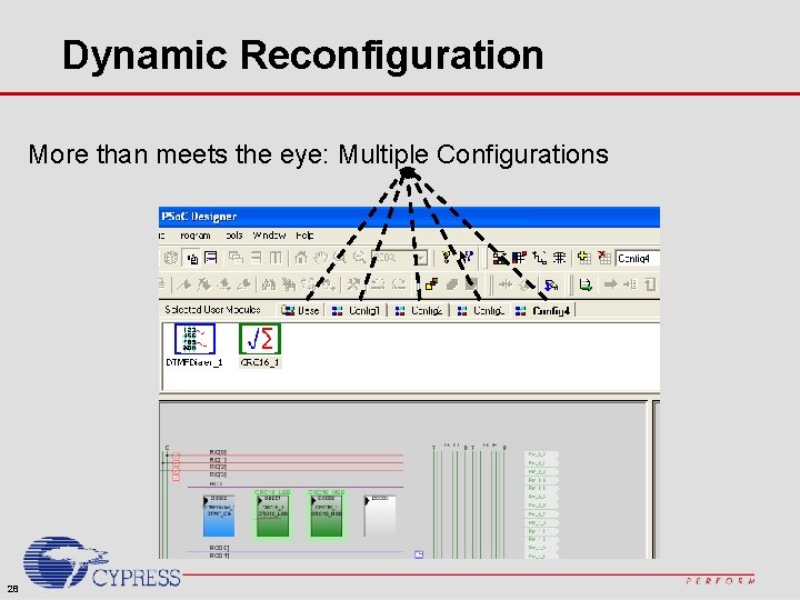
Additional Features • • • 13 Comprehensive Design Tools Intuitive Resource Placement Easy Routing Powerful Logic Dynamic Reconfiguration

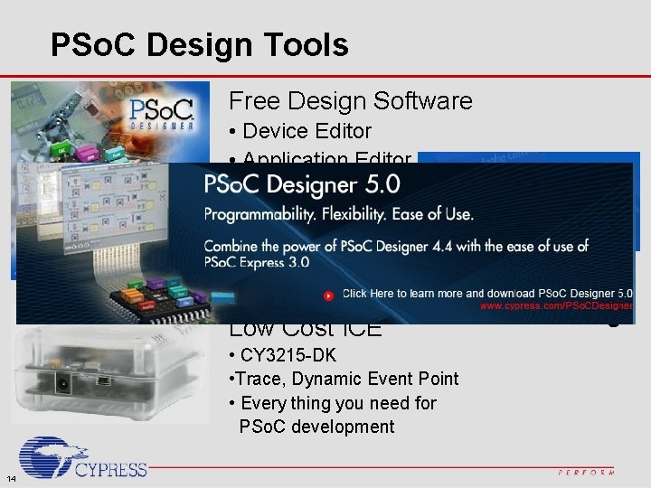
PSo. C Design Tools Free Design Software • Device Editor • Application Editor • C Compiler • Assembler • Librarian Graphical Application • Debugger Design Software…… No MCU Coding! Low Cost ICE • CY 3215 -DK • Trace, Dynamic Event Point • Every thing you need for PSo. C development 14

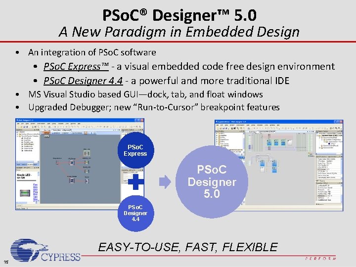
PSo. C® Designer™ 5. 0 A New Paradigm in Embedded Design • An integration of PSo. C software • PSo. C Express™ - a visual embedded code free design environment • PSo. C Designer 4. 4 - a powerful and more traditional IDE • MS Visual Studio based GUI—dock, tab, and float windows • Upgraded Debugger; new “Run-to-Cursor” breakpoint features PSo. C Express PSo. C Designer 5. 0 PSo. C Designer 4. 4 EASY-TO-USE, FAST, FLEXIBLE 15

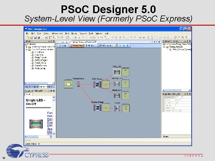
PSo. C Designer 5. 0 System-Level View (Formerly PSo. C Express) 16

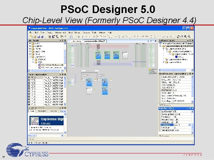
PSo. C Designer 5. 0 Chip-Level View (Formerly PSo. C Designer 4. 4) 17

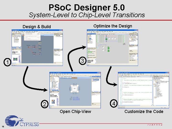
PSo. C Designer 5. 0 System-Level to Chip-Level Transitions Optimize the Design & Build 3 1 4 2 Open Chip-View 18 Customize the Code

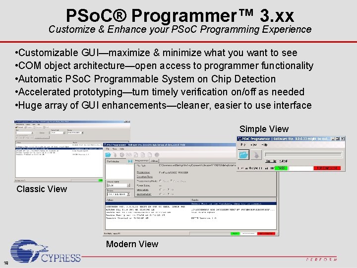
PSo. C® Programmer™ 3. xx Customize & Enhance your PSo. C Programming Experience • Customizable GUI—maximize & minimize what you want to see • COM object architecture—open access to programmer functionality • Automatic PSo. C Programmable System on Chip Detection • Accelerated prototyping—turn timely verification on/off as needed • Huge array of GUI enhancements—cleaner, easier to use interface Simple View Classic View Modern View 19

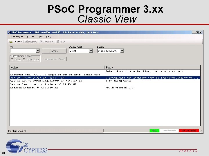
PSo. C Programmer 3. xx Classic View 20

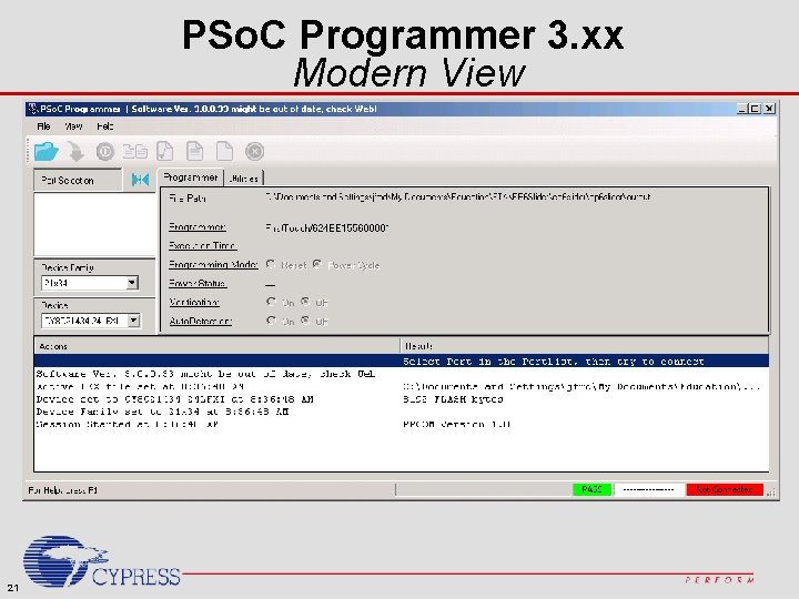
PSo. C Programmer 3. xx Modern View 21

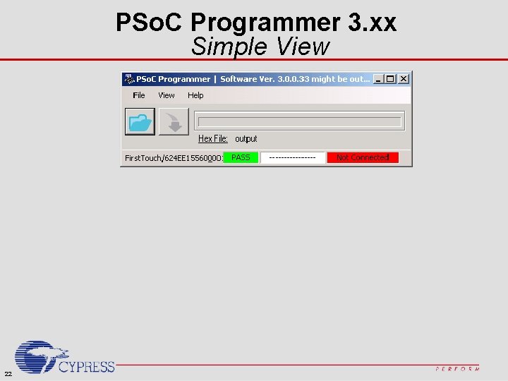
PSo. C Programmer 3. xx Simple View 22

Section 2: PSo. C Designer IDE Software

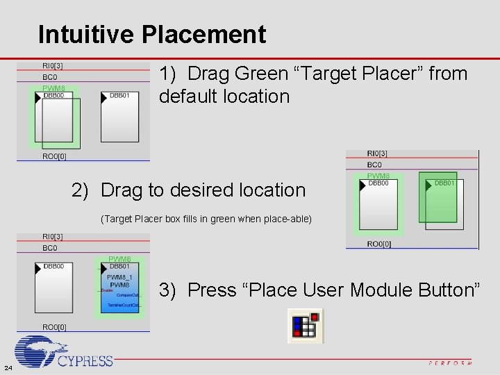
Intuitive Placement 1) Drag Green “Target Placer” from default location 2) Drag to desired location (Target Placer box fills in green when place-able) 3) Press “Place User Module Button” 24

Easy GUI Routing 25

Powerful Combinational Logic 26

Powerful Combinational Logic 27

Dynamic Reconfiguration More than meets the eye: Multiple Configurations 28

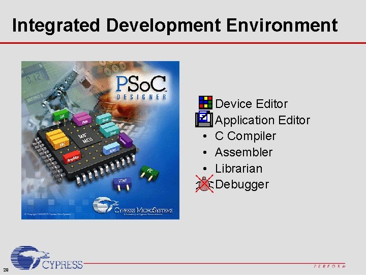
Integrated Development Environment • • • 29 Device Editor Application Editor C Compiler Assembler Librarian Debugger

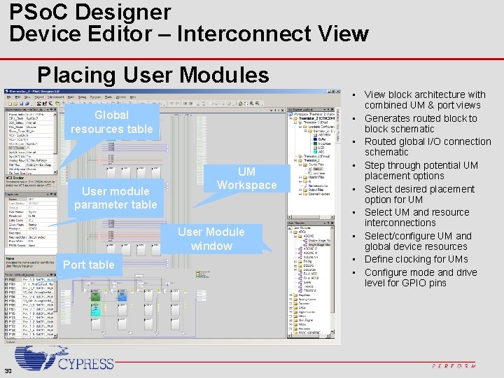
PSo. C Designer Device Editor – Interconnect View Placing User Modules Global resources table User module parameter table UM Workspace User Module window Port table 30 • View block architecture with combined UM & port views • Generates routed block to block schematic • Routed global I/O connection schematic • Step through potential UM placement options • Select desired placement option for UM • Select UM and resource interconnections • Select/configure UM and global device resources • Define clocking for UMs • Configure mode and drive level for GPIO pins

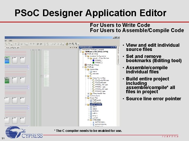
PSo. C Designer Application Editor For Users to Write Code For Users to Assemble/Compile Code • View and edit individual source files • Set and remove bookmarks (Editing tool) • Assemble/compile individual files • Build entire project including assemble/compile* all files in project • Source line error pointer * The C compiler needs to be enabled for use. 31

PSo. C Designer C Compiler The C compiler by Hi Tech is an optional component of the PSo. C Designer IDE. Once enabled, it is fully integrated into the IDE and allows PSo. C Designer to support C source level debugging. Features Include: • ANSI C Compiler • Supports Inline Assembly and can interface with Assembly Modules • Integrated code compressor • Modern Stack-Based Architecture • 7 Basic Data Types Including IEEE 32 -Bit Floating Point • Assembler and Linker • Math and String Libraries • C Interrupt Service Routines • Librarian For more info on the C compiler, please see the C language compiler user guide in the documentation folder of PSo. C Designer. 32

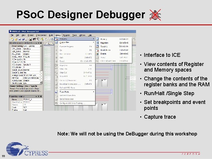
PSo. C Designer Debugger • Interface to ICE • View contents of Register and Memory spaces • Change the contents of the register banks and the RAM • Run/Halt /Single Step • Set breakpoints and event points • Capture trace Note: We will not be using the De. Bugger during this workshop 33

PSo. C Hands On Example Project

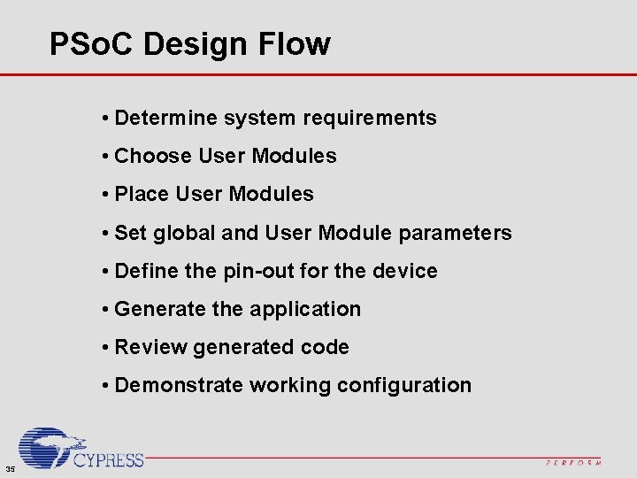
PSo. C Design Flow • Determine system requirements • Choose User Modules • Place User Modules • Set global and User Module parameters • Define the pin-out for the device • Generate the application • Review generated code • Demonstrate working configuration 35

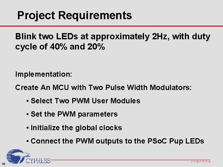
Project Requirements Blink two LEDs at approximately 2 Hz, with duty cycle of 40% and 20% Implementation: Create An MCU with Two Pulse Width Modulators: • Select Two PWM User Modules • Set the PWM parameters • Initialize the global clocks • Connect the PWM outputs to the PSo. C Pup LEDs 36
![Project Implementation Pup PSo C 16 bit PWM 65535 16 P 20 Project Implementation Pup PSo. C 16 -bit PWM ÷ 65535 ÷ 16 P 2[0]](https://slidetodoc.com/presentation_image/57e301a8ccd74541a05eb2ebc452c8fd/image-37.jpg)
Project Implementation Pup PSo. C 16 -bit PWM ÷ 65535 ÷ 16 P 2[0] (94 k. Hz) (1. 5 MHz) 24 MHz (1. 4 Hz) ÷ 16 VC 1 VC 2 16 -bit PWM ÷ 65535 37 (1. 4 Hz) P 2[1]

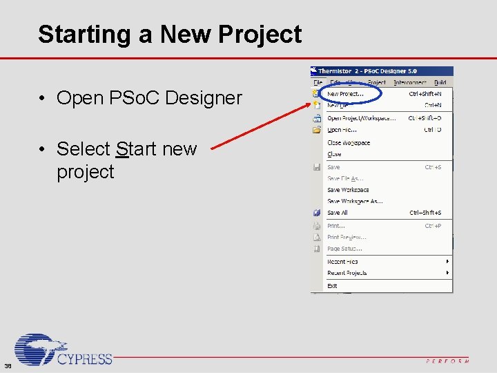
Starting a New Project • Open PSo. C Designer • Select Start new project 38

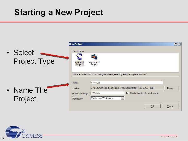
Starting a New Project • Select Project Type • Name The Project 39

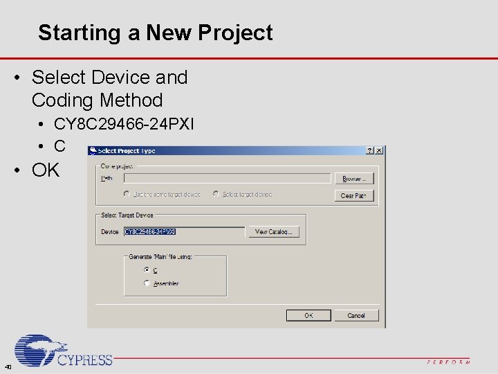
Starting a New Project • Select Device and Coding Method • CY 8 C 29466 -24 PXI • C • OK 40

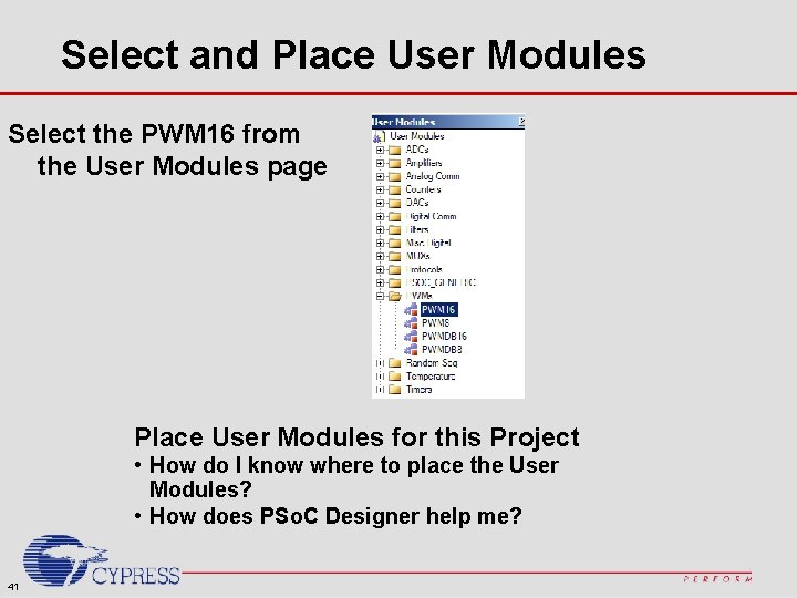
Select and Place User Modules Select the PWM 16 from the User Modules page Place User Modules for this Project • How do I know where to place the User Modules? • How does PSo. C Designer help me? 41

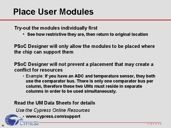
Place User Modules Try-out the modules individually first • See how restrictive they are, then return to original location PSo. C Designer will only allow the modules to be placed where the chip can support them PSo. C Designer will not prevent a placement that may create a conflict for resources • Example: If you have an ADC and temperature sensor, they both use the comparator bus. There is only one comparator bus per column, therefore these two UMs must reside in separate columns in order to be used simultaneously. Read the UM Data Sheets for details Use the Cypress Online Resources • www. cypress. com/support 42

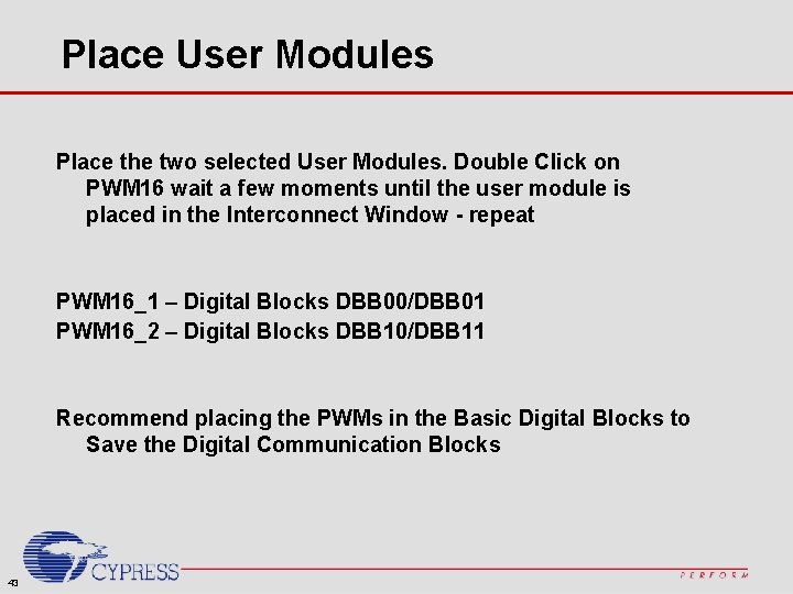
Place User Modules Place the two selected User Modules. Double Click on PWM 16 wait a few moments until the user module is placed in the Interconnect Window - repeat PWM 16_1 – Digital Blocks DBB 00/DBB 01 PWM 16_2 – Digital Blocks DBB 10/DBB 11 Recommend placing the PWMs in the Basic Digital Blocks to Save the Digital Communication Blocks 43

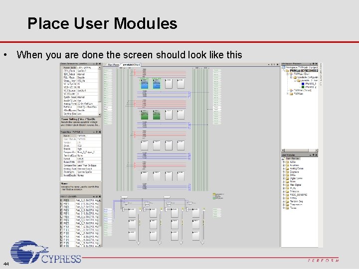
Place User Modules • When you are done the screen should look like this 44

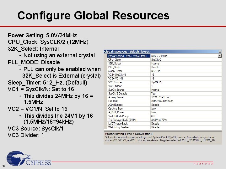
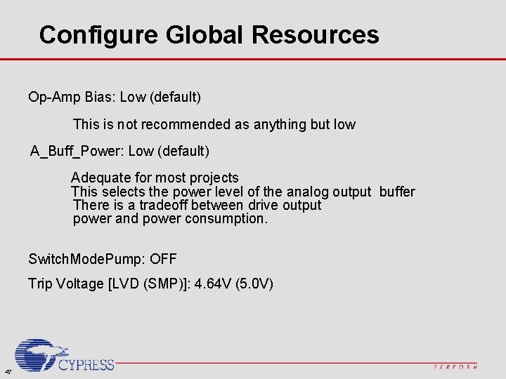
Configure Global Resources Power Setting: 5. 0 V/24 MHz CPU_Clock: Sys. CLK/2 (12 MHz) 32 K_Select: Internal • Not using an external crystal PLL_MODE: Disable • PLL can only be enabled when 32 K_Select is External (crystal) Sleep_Timer: 512_Hz. (Default) VC 1 = Sys. Clk/N: Set to 16 • This divides 24 MHz by 16 = 1. 5 MHz VC 2 = VC 1/N: Set to 16 • This divides the 24 V 1 by 16 (1. 5 MHz/16=94 k. Hz) VC 3 Source: Sys. Clk/1 VC 3 Divider: 1 45

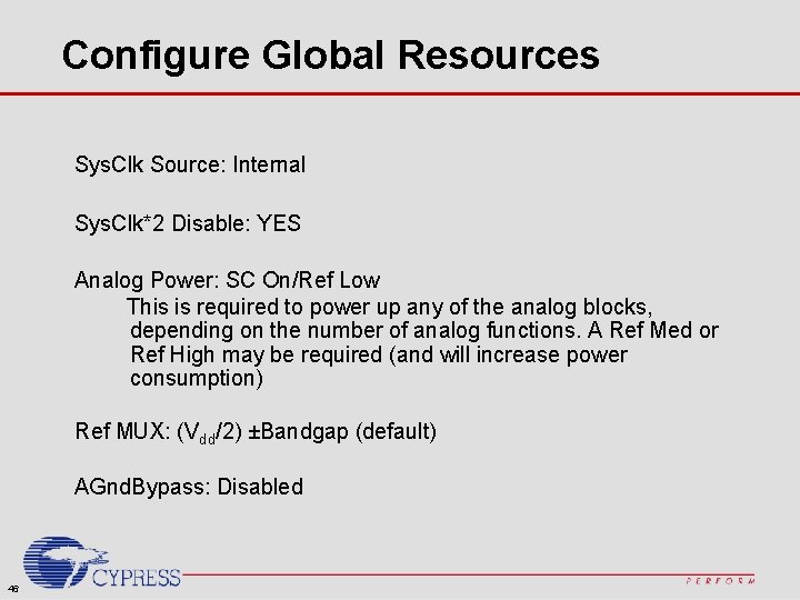
Configure Global Resources Sys. Clk Source: Internal Sys. Clk*2 Disable: YES Analog Power: SC On/Ref Low This is required to power up any of the analog blocks, depending on the number of analog functions. A Ref Med or Ref High may be required (and will increase power consumption) Ref MUX: (Vdd/2) ±Bandgap (default) AGnd. Bypass: Disabled 46

Configure Global Resources Op-Amp Bias: Low (default) This is not recommended as anything but low A_Buff_Power: Low (default) Adequate for most projects This selects the power level of the analog output buffer There is a tradeoff between drive output power and power consumption. Switch. Mode. Pump: OFF Trip Voltage [LVD (SMP)]: 4. 64 V (5. 0 V) 47

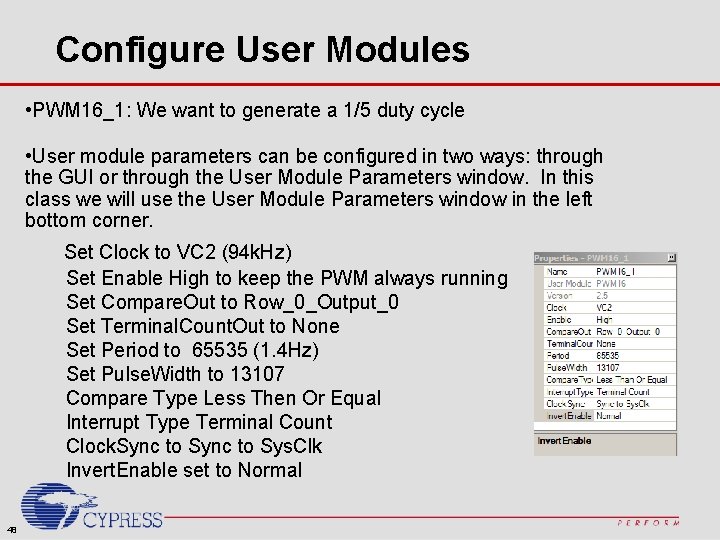
Configure User Modules • PWM 16_1: We want to generate a 1/5 duty cycle • User module parameters can be configured in two ways: through the GUI or through the User Module Parameters window. In this class we will use the User Module Parameters window in the left bottom corner. Set Clock to VC 2 (94 k. Hz) Set Enable High to keep the PWM always running Set Compare. Out to Row_0_Output_0 Set Terminal. Count. Out to None Set Period to 65535 (1. 4 Hz) Set Pulse. Width to 13107 Compare Type Less Then Or Equal Interrupt Type Terminal Count Clock. Sync to Sys. Clk Invert. Enable set to Normal 48

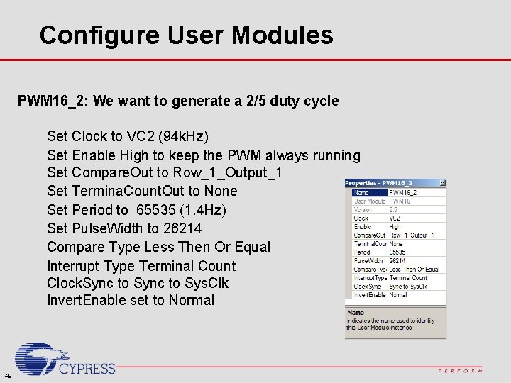
Configure User Modules PWM 16_2: We want to generate a 2/5 duty cycle Set Clock to VC 2 (94 k. Hz) Set Enable High to keep the PWM always running Set Compare. Out to Row_1_Output_1 Set Termina. Count. Out to None Set Period to 65535 (1. 4 Hz) Set Pulse. Width to 26214 Compare Type Less Then Or Equal Interrupt Type Terminal Count Clock. Sync to Sys. Clk Invert. Enable set to Normal 49

Interconnect Blocks to Resources What interconnection possibilities are there? • Data Inputs • Data Outputs • Clocks • Block-to-block When you specify a PSo. C block connection to a pin you are making a physical connection to the hardware of the PSo. C device. 50

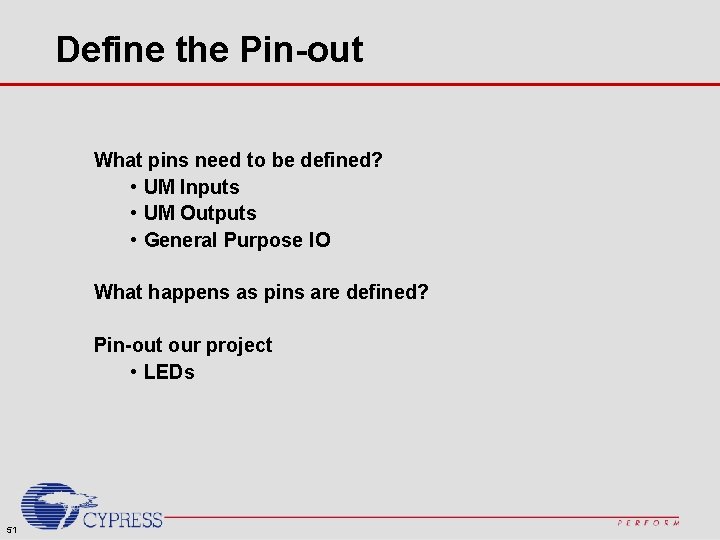
Define the Pin-out What pins need to be defined? • UM Inputs • UM Outputs • General Purpose IO What happens as pins are defined? Pin-out our project • LEDs 51

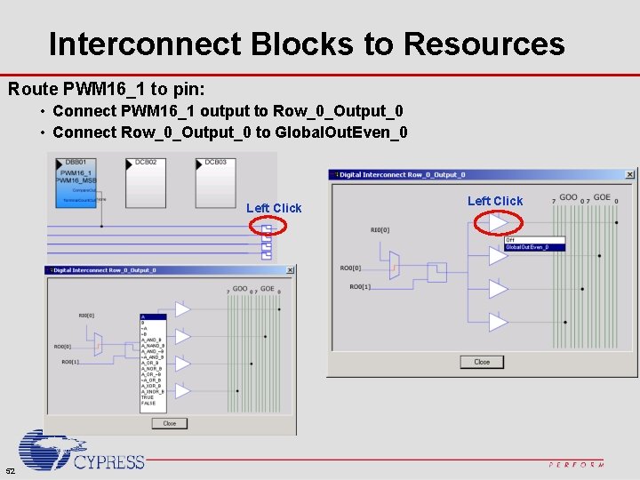
Interconnect Blocks to Resources Route PWM 16_1 to pin: • Connect PWM 16_1 output to Row_0_Output_0 • Connect Row_0_Output_0 to Global. Out. Even_0 Left Click 52 Left Click

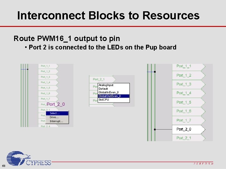
Interconnect Blocks to Resources Route PWM 16_1 output to pin • Port 2 is connected to the LEDs on the Pup board 53

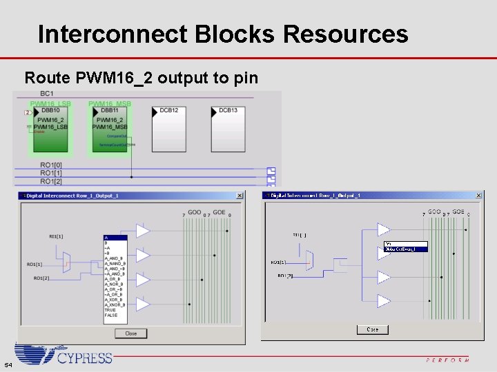
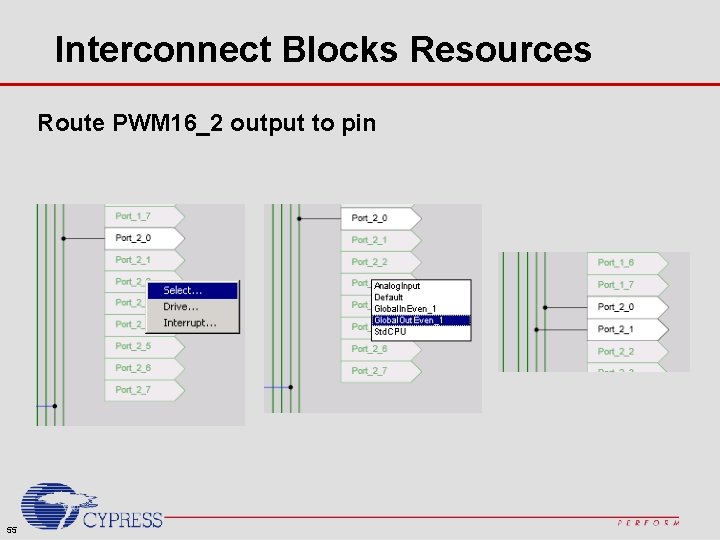
Interconnect Blocks Resources Route PWM 16_2 output to pin 54

Interconnect Blocks Resources Route PWM 16_2 output to pin 55

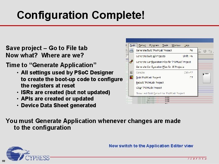
Configuration Complete! Save project – Go to File tab Now what? Where are we? Time to “Generate Application” • All settings used by PSo. C Designer to create the boot-up code to configure the registers at reset • ISRs are created (but not updated) • APIs are created or updated • Device Data Sheet generated You must Generate Application whenever changes are made to the configuration Now switch to the Application Editor view 56

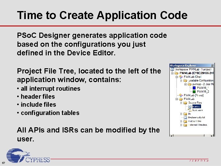
Time to Create Application Code PSo. C Designer generates application code based on the configurations you just defined in the Device Editor. Project File Tree, located to the left of the application window, contains: • all interrupt routines • header files • include files • configuration tables All APIs and ISRs can be modified by the user. 57

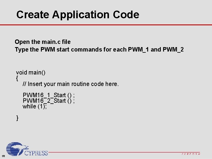
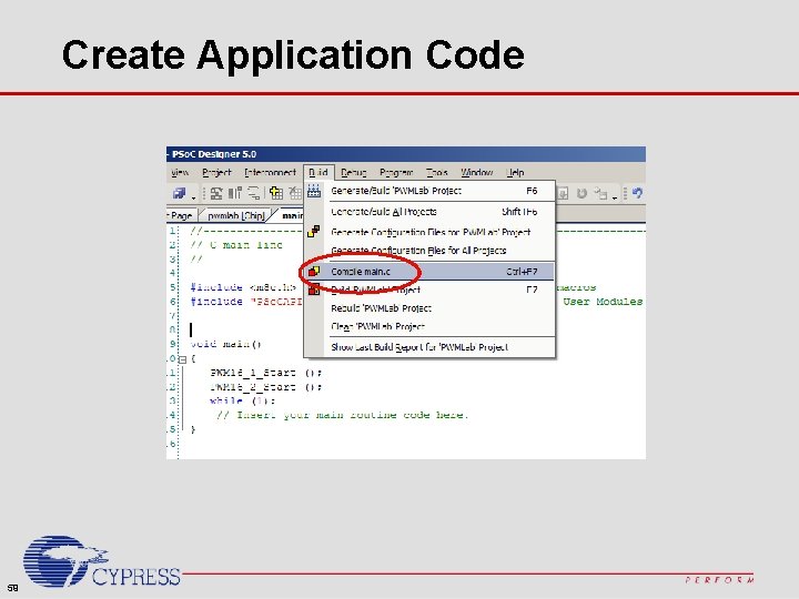
Create Application Code Open the main. c file Type the PWM start commands for each PWM_1 and PWM_2 void main() { // Insert your main routine code here. PWM 16_1_Start () ; PWM 16_2_Start () ; while (1); } 58

Create Application Code 59

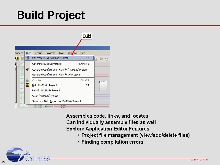
Build Project Assembles code, links, and locates Can individually assemble files as well Explore Application Editor Features • Project file management (view/add/delete files) • Finding compilation errors 60

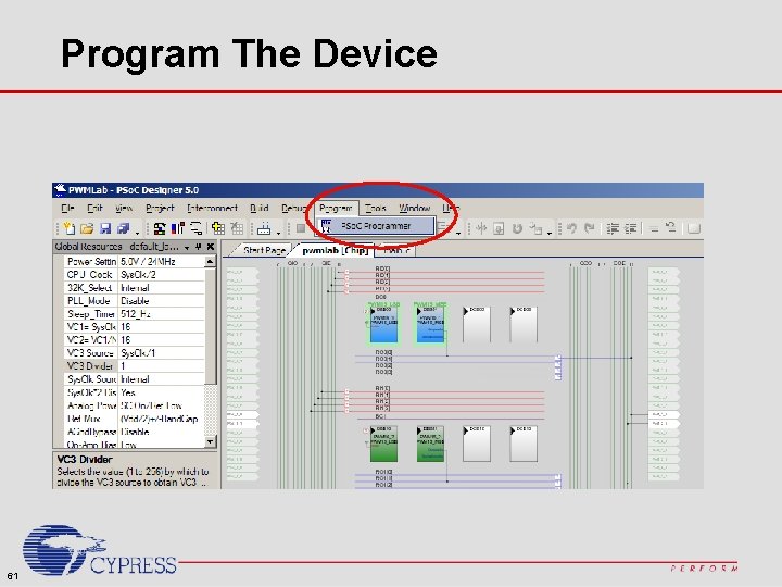
Program The Device 61

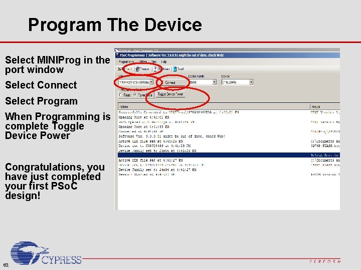
Program The Device Select MINIProg in the port window Select Connect Select Program When Programming is complete Toggle Device Power Congratulations, you have just completed your first PSo. C design! 62

Appendix 63

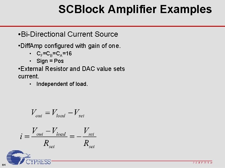
SCBlock Amplifier Examples • Bi-Directional Current Source • Diff. Amp configured with gain of one. • CF=CB=CA=16 • Sign = Pos • External Resistor and DAC value sets current. • Independent of load. 64

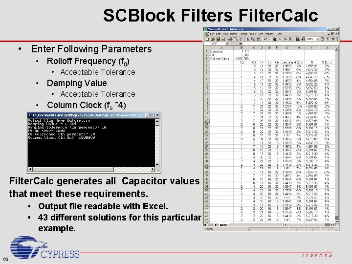
SCBlock Filters Filter. Calc • Enter Following Parameters • Rolloff Frequency (f 0) • Acceptable Tolerance • Damping Value • Acceptable Tolerance • Column Clock (fs *4) Filter. Calc generates all Capacitor values that meet these requirements. s Output file readable with Excel. s 43 different solutions for this particular example. 65

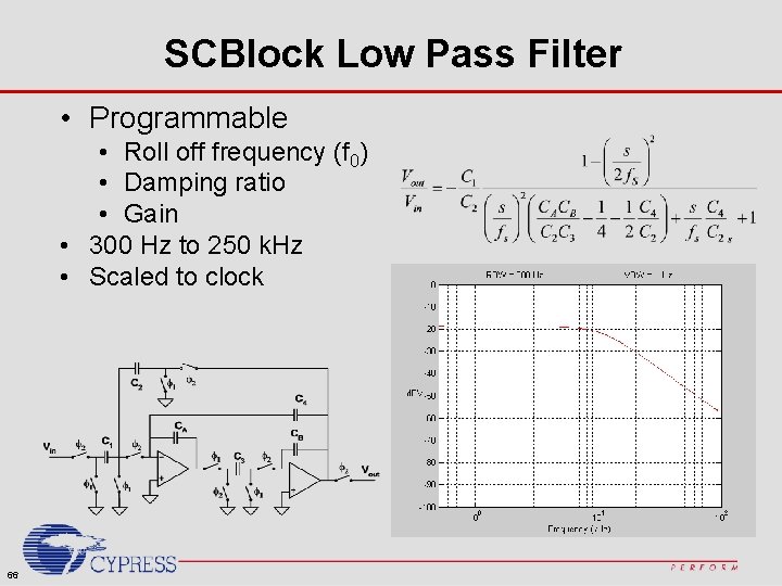
SCBlock Low Pass Filter • Programmable • Roll off frequency (f 0) • Damping ratio • Gain • 300 Hz to 250 k. Hz • Scaled to clock 66

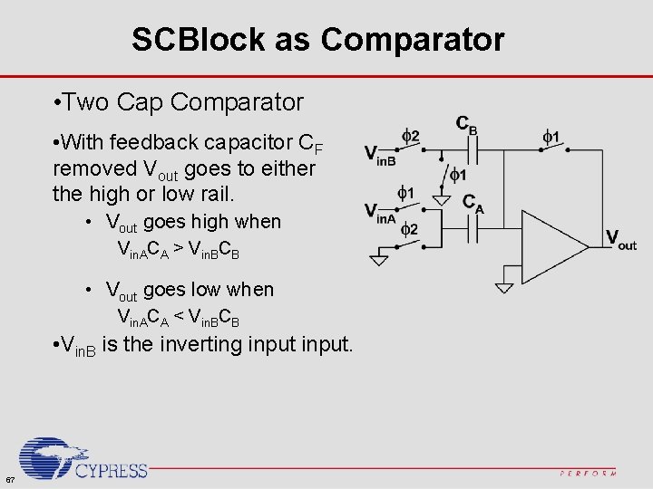
SCBlock as Comparator • Two Cap Comparator • With feedback capacitor CF removed Vout goes to either the high or low rail. • Vout goes high when Vin. ACA > Vin. BCB • Vout goes low when Vin. ACA < Vin. BCB • Vin. B is the inverting input. 67

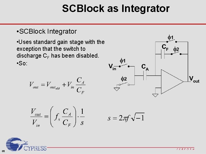
SCBlock as Integrator • SCBlock Integrator • Uses standard gain stage with the exception that the switch to discharge CF has been disabled. • So: 68

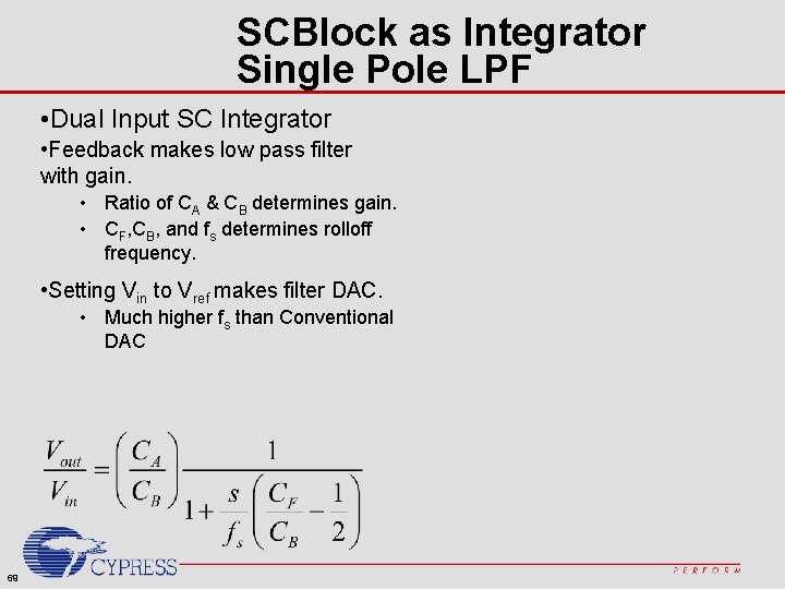
SCBlock as Integrator Single Pole LPF • Dual Input SC Integrator • Feedback makes low pass filter with gain. • Ratio of CA & CB determines gain. • CF, CB, and fs determines rolloff frequency. • Setting Vin to Vref makes filter DAC. • Much higher fs than Conventional DAC 69

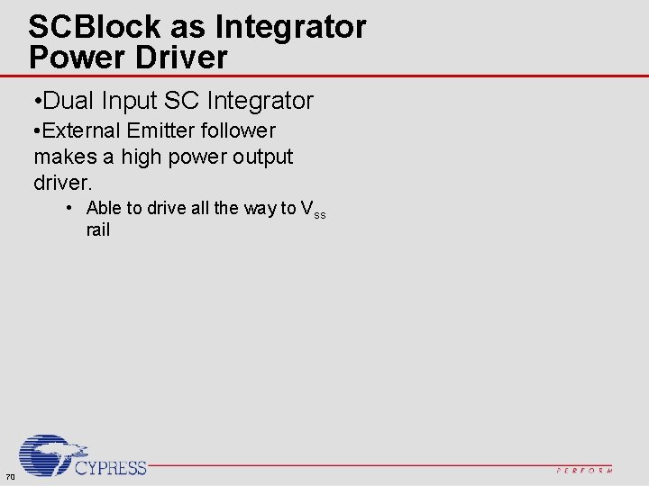
SCBlock as Integrator Power Driver • Dual Input SC Integrator • External Emitter follower makes a high power output driver. • Able to drive all the way to Vss rail 70

SCBlock as Integrator Speaker Driver • Dual Input SC Integrator • Or a 4 Ohm Class B Speaker Driver. 71

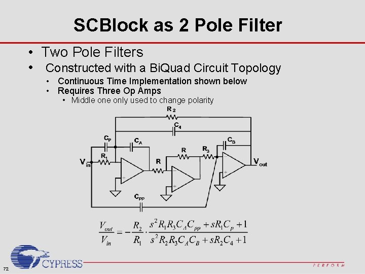
SCBlock as 2 Pole Filter • Two Pole Filters • Constructed with a Bi. Quad Circuit Topology • Continuous Time Implementation shown below • Requires Three Op Amps • Middle only used to change polarity 72

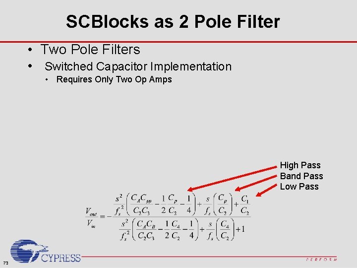
SCBlocks as 2 Pole Filter • Two Pole Filters • Switched Capacitor Implementation • Requires Only Two Op Amps High Pass Band Pass Low Pass 73

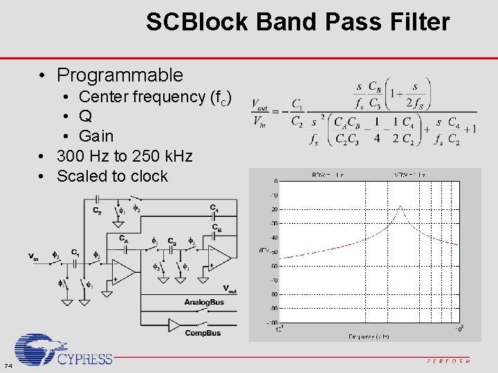
SCBlock Band Pass Filter • Programmable • Center frequency (fc) • Q • Gain • 300 Hz to 250 k. Hz • Scaled to clock 74

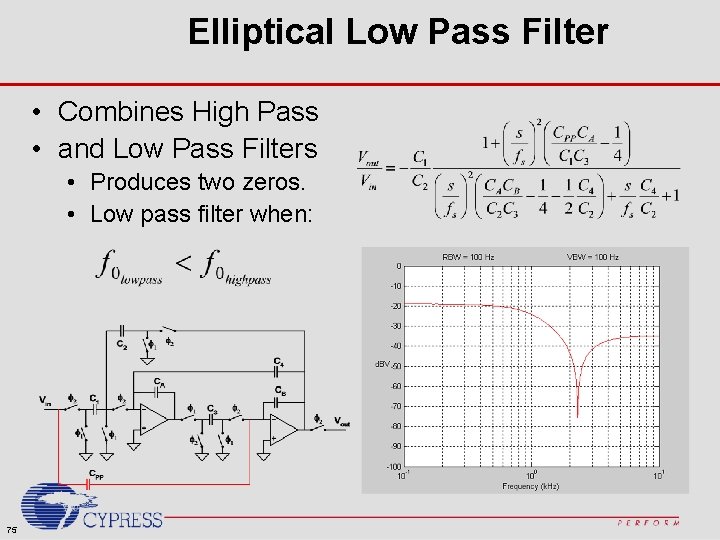
Elliptical Low Pass Filter • Combines High Pass • and Low Pass Filters • Produces two zeros. • Low pass filter when: 75

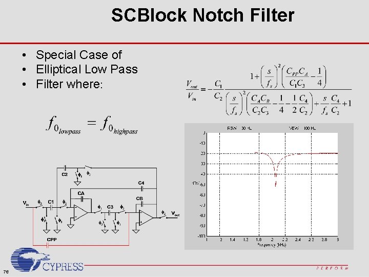
SCBlock Notch Filter • Special Case of • Elliptical Low Pass • Filter where: 76