PSo C 3 PSo C 5 102 System
- Slides: 50

PSo. C 3 / PSo. C 5 102: System Resources Introduction to PSo. C 3 / PSo. C 5 Workshop – Rev *H 1

Section Objectives, you will be able to: • Understand the system block diagram of PSo. C 3 / PSo. C 5 devices • Understand use the PSo. C 3 / PSo. C 5 System Resources, including: Power system Programming & debugging Configuration and boot process Resets Clocking Memory & mapping DMA and PHUB I/O Interrupts Introduction to PSo. C 3 / PSo. C 5 Workshop – Rev *H 2

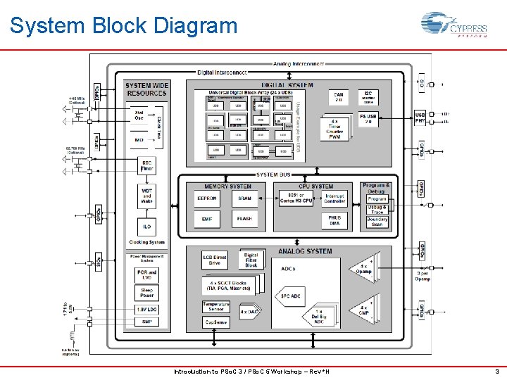
System Block Diagram Introduction to PSo. C 3 / PSo. C 5 Workshop – Rev *H 3

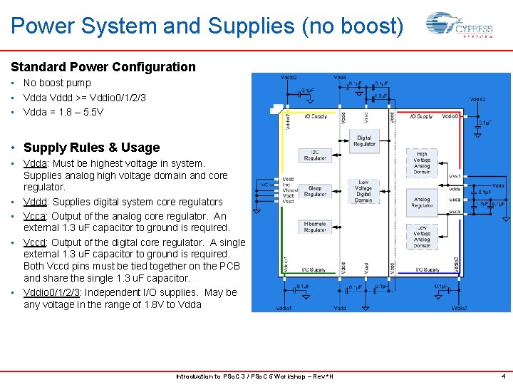
Power System and Supplies (no boost) Standard Power Configuration • No boost pump • Vdda Vddd >= Vddio 0/1/2/3 • Vdda = 1. 8 – 5. 5 V • Supply Rules & Usage • Vdda: Must be highest voltage in system. Supplies analog high voltage domain and core regulator. • Vddd: Supplies digital system core regulators • Vcca: Output of the analog core regulator. An external 1. 3 u. F capacitor to ground is required. • Vccd: Output of the digital core regulator. A single external 1. 3 u. F capacitor to ground is required. Both Vccd pins must be tied together on the PCB and share the single 1. 3 u. F capacitor. • Vddio 0/1/2/3: Independent I/O supplies. May be any voltage in the range of 1. 8 V to Vdda Introduction to PSo. C 3 / PSo. C 5 Workshop – Rev *H 4

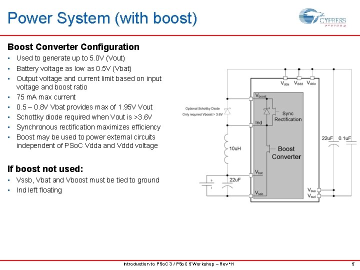
Power System (with boost) Boost Converter Configuration • Used to generate up to 5. 0 V (Vout) • Battery voltage as low as 0. 5 V (Vbat) • Output voltage and current limit based on input voltage and boost ratio • 75 m. A max current • 0. 5 – 0. 8 V Vbat provides max of 1. 95 V Vout • Schottky diode required when Vout is >3. 6 V • Synchronous rectification maximizes efficiency • Boost may be used to power external circuits independent of PSo. C Vdda and Vddd voltage If boost not used: • Vssb, Vbat and Vboost must be tied to ground • Ind left floating Introduction to PSo. C 3 / PSo. C 5 Workshop – Rev *H 5

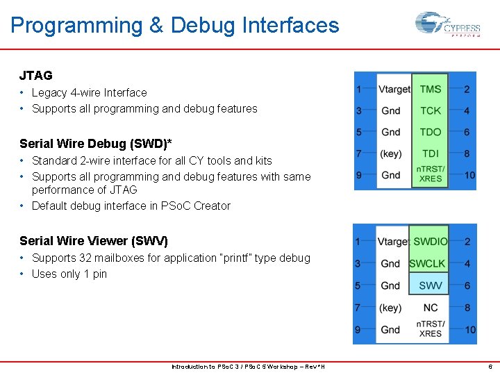
Programming & Debug Interfaces JTAG • Legacy 4 -wire Interface • Supports all programming and debug features Serial Wire Debug (SWD)* • Standard 2 -wire interface for all CY tools and kits • Supports all programming and debug features with same performance of JTAG • Default debug interface in PSo. C Creator Serial Wire Viewer (SWV) • Supports 32 mailboxes for application “printf” type debug • Uses only 1 pin Introduction to PSo. C 3 / PSo. C 5 Workshop – Rev *H 6

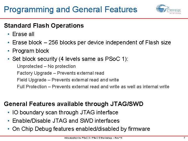
Programming and General Features Standard Flash Operations • • Erase all Erase block – 256 blocks per device independent of Flash size Program block Set block security (4 levels same as PSo. C 1): Unprotected – No protection Factory Upgrade – Prevents external read Field Upgrade – Prevents external read and write Full Protection – Prevents external read and write as well as internal write General Features available through JTAG/SWD • IO boundary scan through JTAG interface • Enable/Disable JTAG and SWD interfaces • On Chip Debug features enabled/disabled by firmware Introduction to PSo. C 3 / PSo. C 5 Workshop – Rev *H 7

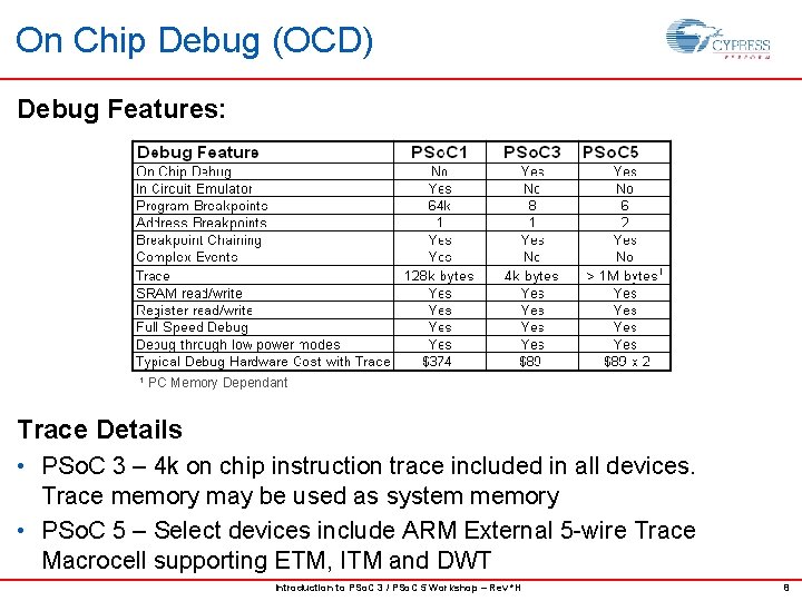
On Chip Debug (OCD) Debug Features: 1 PC Memory Dependant Trace Details • PSo. C 3 – 4 k on chip instruction trace included in all devices. Trace memory may be used as system memory • PSo. C 5 – Select devices include ARM External 5 -wire Trace Macrocell supporting ETM, ITM and DWT Introduction to PSo. C 3 / PSo. C 5 Workshop – Rev *H 8

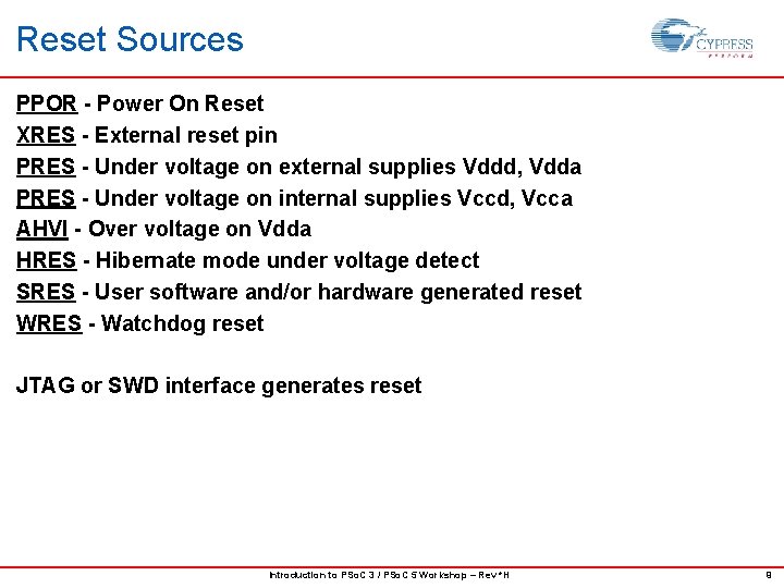
Reset Sources PPOR - Power On Reset XRES - External reset pin PRES - Under voltage on external supplies Vddd, Vdda PRES - Under voltage on internal supplies Vccd, Vcca AHVI - Over voltage on Vdda HRES - Hibernate mode under voltage detect SRES - User software and/or hardware generated reset WRES - Watchdog reset JTAG or SWD interface generates reset Introduction to PSo. C 3 / PSo. C 5 Workshop – Rev *H 9

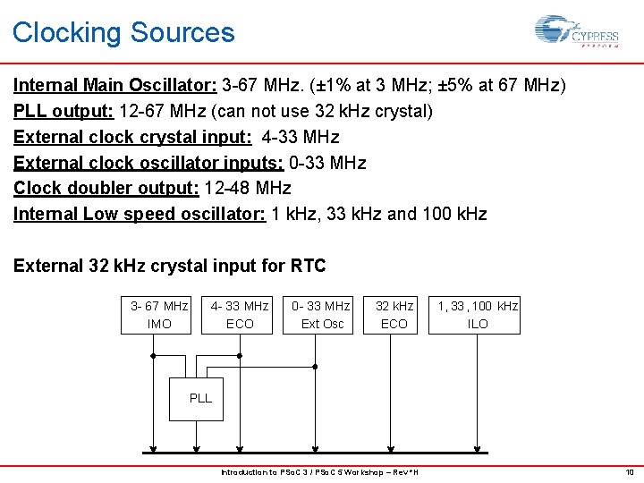
Clocking Sources Internal Main Oscillator: 3 -67 MHz. (± 1% at 3 MHz; ± 5% at 67 MHz) PLL output: 12 -67 MHz (can not use 32 k. Hz crystal) External clock crystal input: 4 -33 MHz External clock oscillator inputs: 0 -33 MHz Clock doubler output: 12 -48 MHz Internal Low speed oscillator: 1 k. Hz, 33 k. Hz and 100 k. Hz External 32 k. Hz crystal input for RTC 3 - 67 MHz IMO 4 - 33 MHz ECO 0 - 33 MHz Ext Osc 32 k. Hz ECO 1, 33 , 100 k. Hz ILO PLL Introduction to PSo. C 3 / PSo. C 5 Workshop – Rev *H 10

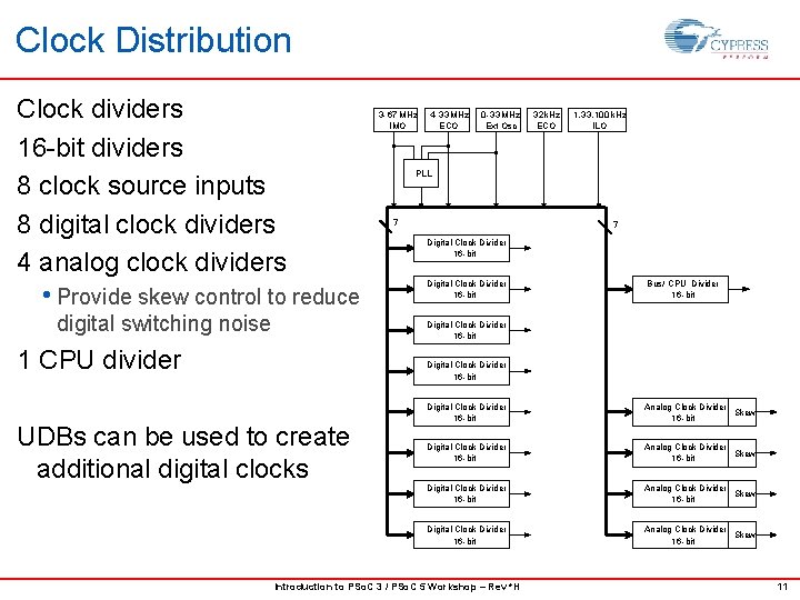
Clock Distribution Clock dividers 16 -bit dividers 8 clock source inputs 8 digital clock dividers 4 analog clock dividers • Provide skew control to reduce digital switching noise 3 - 67 MHz IMO 4 - 33 MHz ECO 0 - 33 MHz Ext Osc 32 k. Hz ECO 1, 33, 100 k. Hz ILO PLL 7 7 Digital Clock Divider 16 -bit Bus/ CPU Divider 16 -bit Digital Clock Divider 16 -bit 1 CPU divider Digital Clock Divider 16 -bit UDBs can be used to create additional digital clocks Digital Clock Divider 16 -bit Analog Clock Divider Skew 16 -bit Introduction to PSo. C 3 / PSo. C 5 Workshop – Rev *H 11

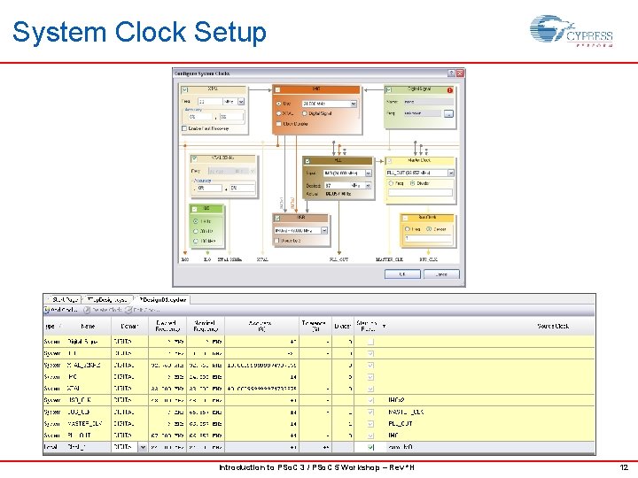
System Clock Setup Introduction to PSo. C 3 / PSo. C 5 Workshop – Rev *H 12

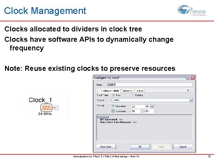
Clock Management Clocks allocated to dividers in clock tree Clocks have software APIs to dynamically change frequency Note: Reuse existing clocks to preserve resources Introduction to PSo. C 3 / PSo. C 5 Workshop – Rev *H 13

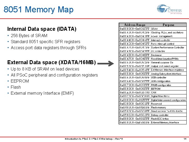
8051 Memory Map Internal Data space (IDATA) • 256 Bytes of SRAM • Standard 8051 specific SFR registers • Access port data registers through SFRs External Data space (XDATA/16 MB) • • • Up to 8 KB of SRAM on lead devices All PSo. C peripheral and configuration registers EEPROM Flash External memory Interface (EMIF) Introduction to PSo. C 3 / PSo. C 5 Workshop – Rev *H 14

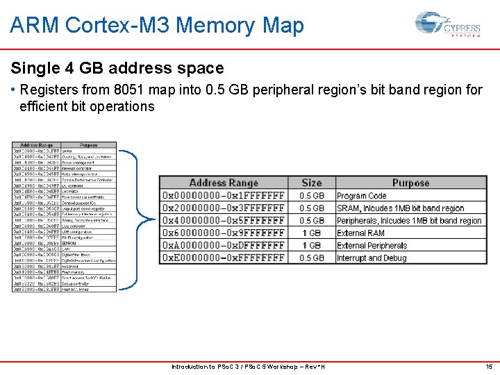
ARM Cortex-M 3 Memory Map Single 4 GB address space • Registers from 8051 map into 0. 5 GB peripheral region’s bit band region for efficient bit operations Introduction to PSo. C 3 / PSo. C 5 Workshop – Rev *H 15

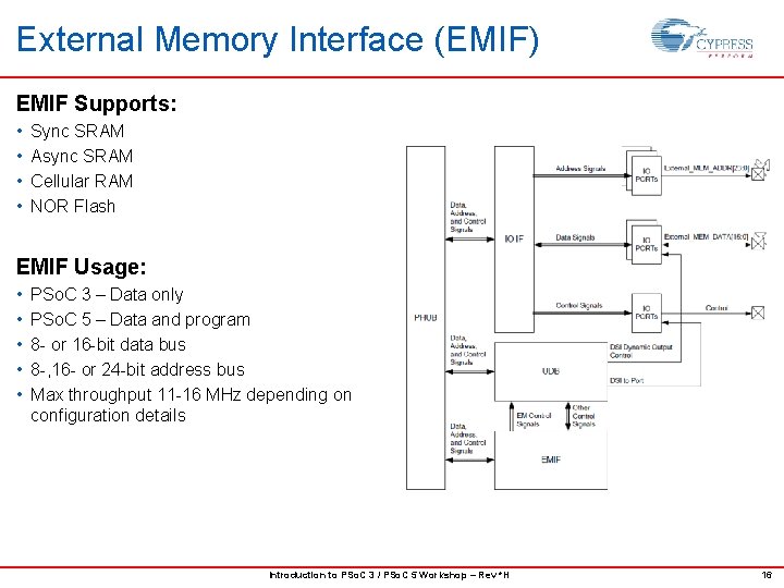
External Memory Interface (EMIF) EMIF Supports: • • Sync SRAM Async SRAM Cellular RAM NOR Flash EMIF Usage: • • • PSo. C 3 – Data only PSo. C 5 – Data and program 8 - or 16 -bit data bus 8 -, 16 - or 24 -bit address bus Max throughput 11 -16 MHz depending on configuration details Introduction to PSo. C 3 / PSo. C 5 Workshop – Rev *H 16

Software Use of Registers 8051 and ARM Cortex-M 3 • Provide same functionality/address mapping to all PSo. C 3 / PSo. C 5 registers • Use Peripheral Hub (PHUB) bus Macros hide MCU/compiler differences enabling PSo. C 3 / PSo. C 5 portability • cytypes. h CY_GET_REG 8(addr) CY_SET_REG 8(addr, value) • cydevice_trm. h Contains device register #defines 8051 includes SFR registers allowing direct register access • Affects portability to PSo. C 5 if used • PSo. C 3_8051. h Contains SFR register #defines Introduction to PSo. C 3 / PSo. C 5 Workshop – Rev *H 17

Flash Blocks: • 256 Blocks in all devices – 64 KB flash has 256 byte block size • Each block may be set to 1 of 4 protection levels of increasing security Unprotected – Allows internal and external reads and writes Factory Upgrade – Prevents external read Field Upgrade – Prevents external read and write Full Protection – Prevents external read and write as well as internal write • Flash is erased and programmed in block units Specs: • Code executes out of Flash • Flash-writes block CPU unless executing from cache (PSo. C 5 only) • 20 year minimum retention • 10 k minimum endurance • 15 ms block erase + write time Introduction to PSo. C 3 / PSo. C 5 Workshop – Rev *H 18

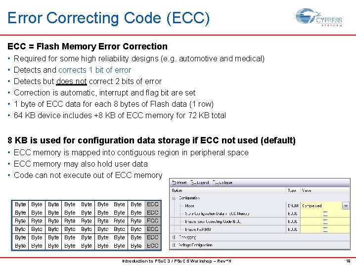
Error Correcting Code (ECC) ECC = Flash Memory Error Correction • • • Required for some high reliability designs (e. g. automotive and medical) Detects and corrects 1 bit of error Detects but does not correct 2 bits of error Correction is automatic, interrupt and flag bit are set 1 byte of ECC data for each 8 bytes of Flash data (1 row) 64 KB device includes +8 KB of ECC memory for 72 KB total 8 KB is used for configuration data storage if ECC not used (default) • ECC memory is mapped into contiguous region in peripheral space • ECC memory may also hold user data • Code can not execute out of ECC memory Introduction to PSo. C 3 / PSo. C 5 Workshop – Rev *H 19

EEPROM 2 KB of EEPROM are provided Code can not execute out of EEPROM Specs: • EEPROM writes do not block CPU execution • 20 year minimum retention • 100 k minimum endurance • 2 ms single byte erase + write time • Supports single byte erase and writes • May erase or write up to 16 consecutive bytes (1 row) at the same time. Introduction to PSo. C 3 / PSo. C 5 Workshop – Rev *H 20

Nonvolatile Latches (NV latches) NV Latches • • Single Flash bits used to hold critical configuration data Required at power up before normal Flash can be read Used the same as fuse bits except resettable Uniquely capable of asynchronously outputting the bit state immediately on POR release NV Latch Specs: • • 10 minimum endurance (Like fuse bits, not programmed often) 20 year minimum retention Set as required by PSo. C Creator (System tab of DWRM) NV Latches are used for: Each IO Port’s initial reset state (High-Z, pull-up, pull-down) Optional XRES pin (P 1[2]) enable Configuration Speed (fast, slow) Debug Port Selection (4 -wire JTAG, 5 -wire JTAG, SWD, None) Error Correcting Code (ECC) enable Digital clock phase delay (2. 5 – 12. 5 ns) Introduction to PSo. C 3 / PSo. C 5 Workshop – Rev *H 21

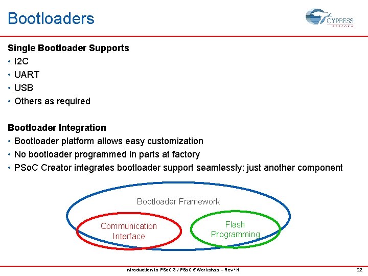
Bootloaders Single Bootloader Supports • I 2 C • UART • USB • Others as required Bootloader Integration • Bootloader platform allows easy customization • No bootloader programmed in parts at factory • PSo. C Creator integrates bootloader support seamlessly; just another component Bootloader Framework Communication Interface Flash Programming Introduction to PSo. C 3 / PSo. C 5 Workshop – Rev *H 22

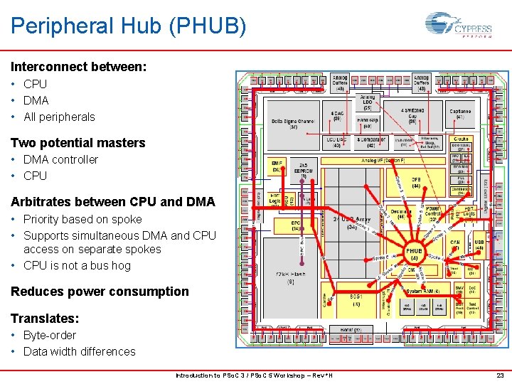
Peripheral Hub (PHUB) Interconnect between: • CPU • DMA • All peripherals Two potential masters • DMA controller • CPU Arbitrates between CPU and DMA • Priority based on spoke • Supports simultaneous DMA and CPU access on separate spokes • CPU is not a bus hog Reduces power consumption Translates: • Byte-order • Data width differences Introduction to PSo. C 3 / PSo. C 5 Workshop – Rev *H 23

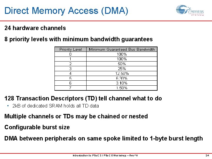
Direct Memory Access (DMA) 24 hardware channels 8 priority levels with minimum bandwidth guarantees 128 Transaction Descriptors (TD) tell channel what to do • 2 k. B of dedicated SRAM holds all TD data Multiple channels or TDs may be chained or nested Configurable burst size DMA between peripherals on same spoke limited to 1 -byte burst length Introduction to PSo. C 3 / PSo. C 5 Workshop – Rev *H 24

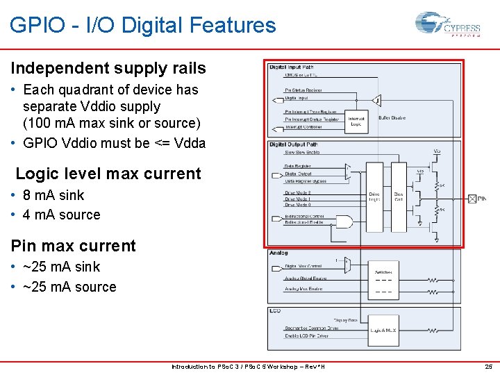
GPIO - I/O Digital Features Independent supply rails • Each quadrant of device has separate Vddio supply (100 m. A max sink or source) • GPIO Vddio must be <= Vdda Logic level max current • 8 m. A sink • 4 m. A source Pin max current • ~25 m. A sink • ~25 m. A source Introduction to PSo. C 3 / PSo. C 5 Workshop – Rev *H 25

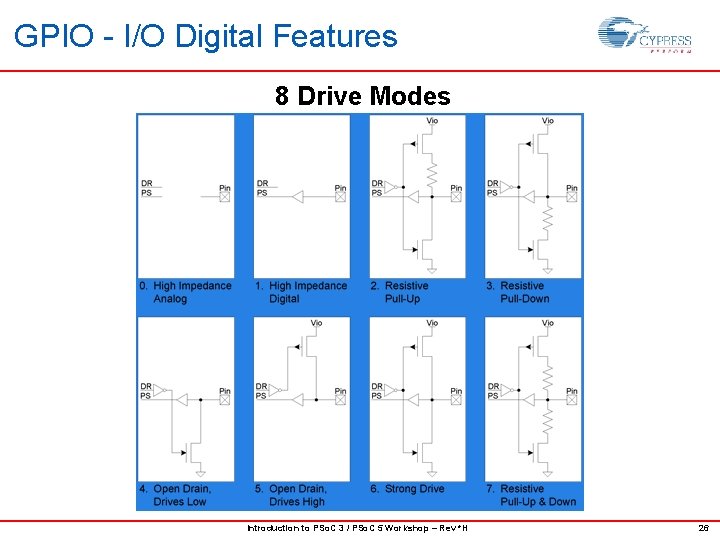
GPIO - I/O Digital Features 8 Drive Modes Introduction to PSo. C 3 / PSo. C 5 Workshop – Rev *H 26

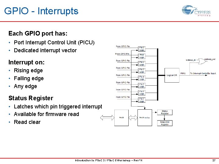
GPIO - Interrupts Each GPIO port has: • Port Interrupt Control Unit (PICU) • Dedicated interrupt vector Interrupt on: • Rising edge • Falling edge • Any edge Status Register • Latches which pin triggered interrupt • Available for firmware read • Read clear Introduction to PSo. C 3 / PSo. C 5 Workshop – Rev *H 27

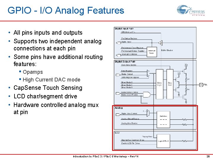
GPIO - I/O Analog Features • All pins inputs and outputs • Supports two independent analog connections at each pin • Some pins have additional routing features: • Opamps • High Current DAC mode • Cap. Sense Touch Sensing • LCD char/segment drive • Hardware controlled analog mux at pin Introduction to PSo. C 3 / PSo. C 5 Workshop – Rev *H 28

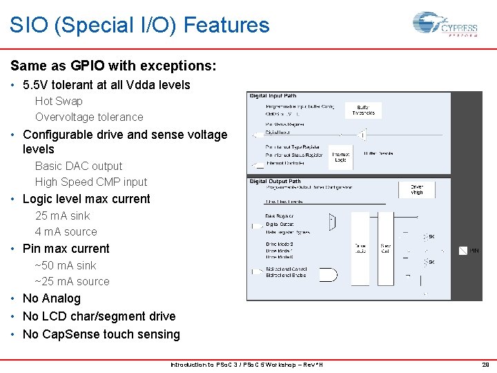
SIO (Special I/O) Features Same as GPIO with exceptions: • 5. 5 V tolerant at all Vdda levels Hot Swap Overvoltage tolerance • Configurable drive and sense voltage levels Basic DAC output High Speed CMP input • Logic level max current 25 m. A sink 4 m. A source • Pin max current ~50 m. A sink ~25 m. A source • No Analog • No LCD char/segment drive • No Cap. Sense touch sensing Introduction to PSo. C 3 / PSo. C 5 Workshop – Rev *H 29

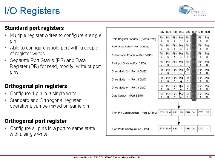
I/O Registers Standard port registers • Multiple register writes to configure a single pin • Able to configure whole port with a couple of register writes • Separate Port Status (PS) and Data Register (DR) for read, modify, write of port pins Orthogonal pin registers • Configure 1 pin in a single write • Standard and Orthogonal register operations can be mixed on same pin Orthogonal port register • Configure all pins in a port to same state with a single write Introduction to PSo. C 3 / PSo. C 5 Workshop – Rev *H 30

Software Use of I/O Registers PHUB Bus Register Macros: • cytypes. h - Contains register macro definitions • cydevice_trm. h - Contains device register definitions Port = CY_GET_REG 8(CYREG_PRT 0_DR); CY_SET_REG 8(CYREG_PRT 0_DR, 0 x 04); Use of SFR registers for 8051 provides direct register access, limits portability • PSo. C 3_8051. h - Contains SFR register #defines SFRPRT 0 DR |= 0 x 04; 8051 provides efficient bit operations on port SFR registers sbit b. Led 1 = SFRPRT 0 DR ^ 3; b. Led 1 = 1; Pin Component provides APIs like any other component • • • Pin_1_Write(); Pin_1_Read. Data. Reg(); Pin_1_Set. Drive. Mode(); Pin_1_Clearinterrupt(); Introduction to PSo. C 3 / PSo. C 5 Workshop – Rev *H 31

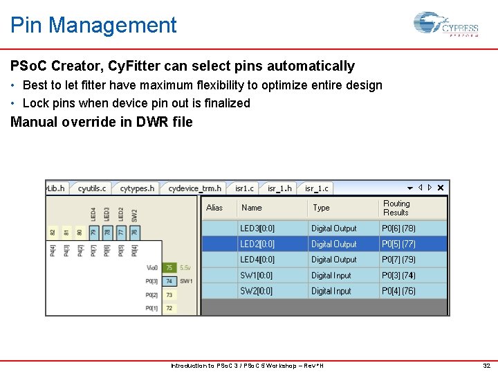
Pin Management PSo. C Creator, Cy. Fitter can select pins automatically • Best to let fitter have maximum flexibility to optimize entire design • Lock pins when device pin out is finalized Manual override in DWR file Introduction to PSo. C 3 / PSo. C 5 Workshop – Rev *H 32

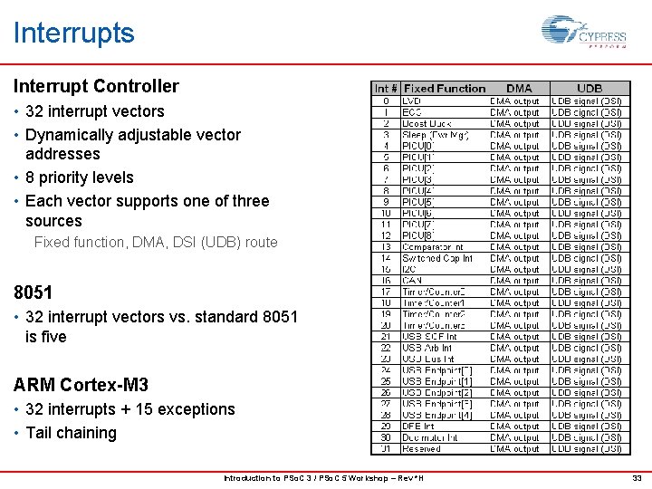
Interrupts Interrupt Controller • 32 interrupt vectors • Dynamically adjustable vector addresses • 8 priority levels • Each vector supports one of three sources Fixed function, DMA, DSI (UDB) route 8051 • 32 interrupt vectors vs. standard 8051 is five ARM Cortex-M 3 • 32 interrupts + 15 exceptions • Tail chaining Introduction to PSo. C 3 / PSo. C 5 Workshop – Rev *H 33

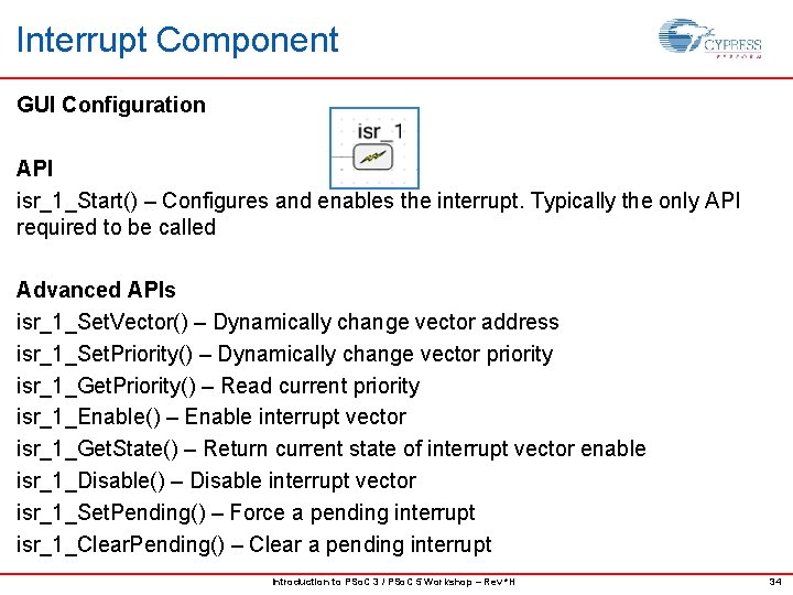
Interrupt Component GUI Configuration API isr_1_Start() – Configures and enables the interrupt. Typically the only API required to be called Advanced APIs isr_1_Set. Vector() – Dynamically change vector address isr_1_Set. Priority() – Dynamically change vector priority isr_1_Get. Priority() – Read current priority isr_1_Enable() – Enable interrupt vector isr_1_Get. State() – Return current state of interrupt vector enable isr_1_Disable() – Disable interrupt vector isr_1_Set. Pending() – Force a pending interrupt isr_1_Clear. Pending() – Clear a pending interrupt Introduction to PSo. C 3 / PSo. C 5 Workshop – Rev *H 34

Review You should now be able to: • Understand the system block diagram of PSo. C 3 / PSo. C 5 devices • Understand use the PSo. C 3 / PSo. C 5 System Resources, including: Power system Programming & debugging Configuration and boot process Resets Clocking Memory & mapping DMA and PHUB I/O Interrupts Introduction to PSo. C 3 / PSo. C 5 Workshop – Rev *H 35

Lab 1 102: My First PSo. C 3 Analog Design Introduction to PSo. C 3 / PSo. C 5 Workshop – Rev *H 36

Lab Objectives: • Acquire an analog signal from the on board accelerometer and it to display LEDS as a carpenter’s level. • More experience with the PSo. C Creator Design Flow Introduction to PSo. C 3 / PSo. C 5 Workshop – Rev *H 37

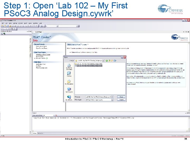
Step 1: Open ‘Lab 102 – My First PSo. C 3 Analog Design. cywrk’ Introduction to PSo. C 3 / PSo. C 5 Workshop – Rev *H 38

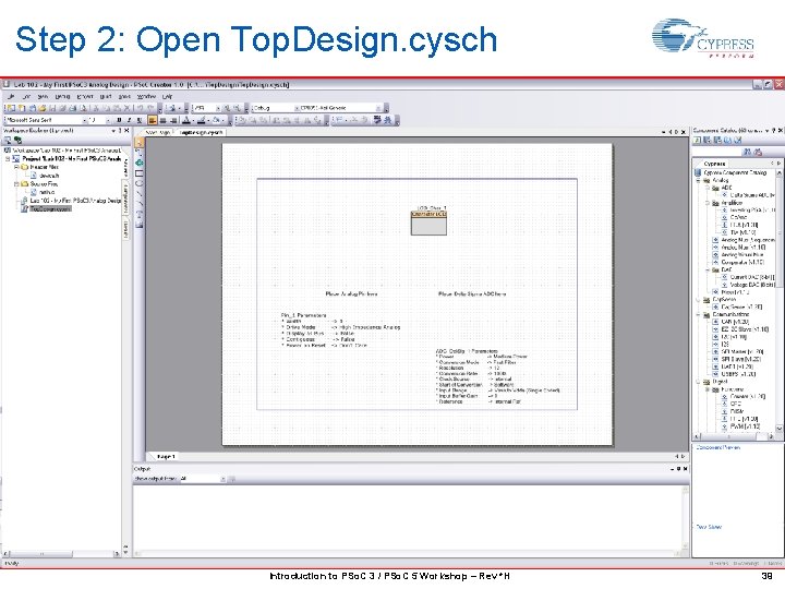
Step 2: Open Top. Design. cysch Introduction to PSo. C 3 / PSo. C 5 Workshop – Rev *H 39

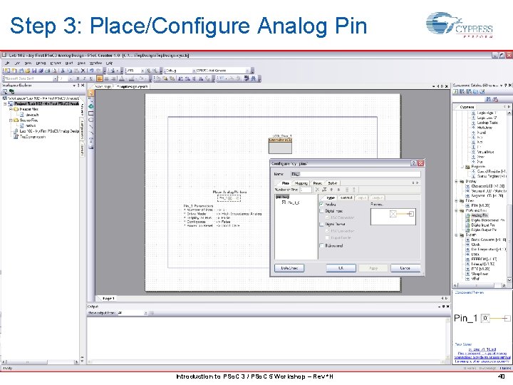
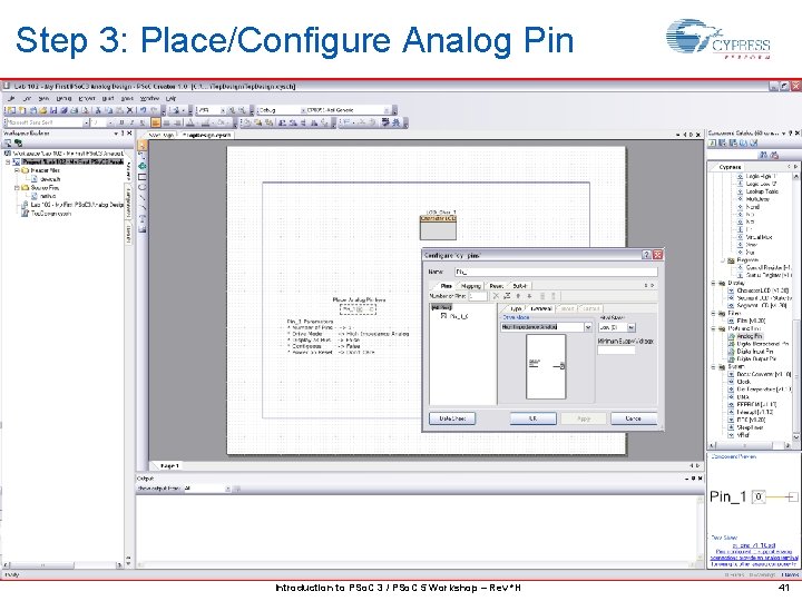
Step 3: Place/Configure Analog Pin Introduction to PSo. C 3 / PSo. C 5 Workshop – Rev *H 40

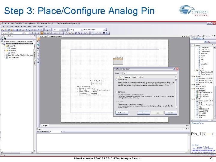
Step 3: Place/Configure Analog Pin Introduction to PSo. C 3 / PSo. C 5 Workshop – Rev *H 41

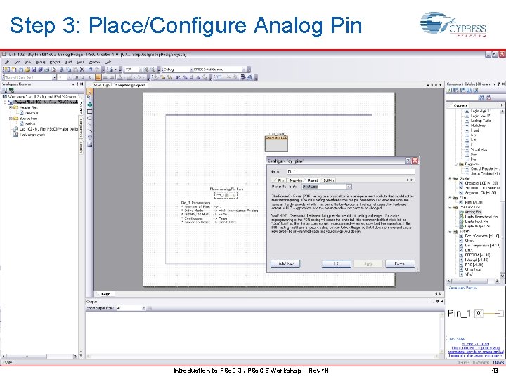
Step 3: Place/Configure Analog Pin Introduction to PSo. C 3 / PSo. C 5 Workshop – Rev *H 42

Step 3: Place/Configure Analog Pin Introduction to PSo. C 3 / PSo. C 5 Workshop – Rev *H 43

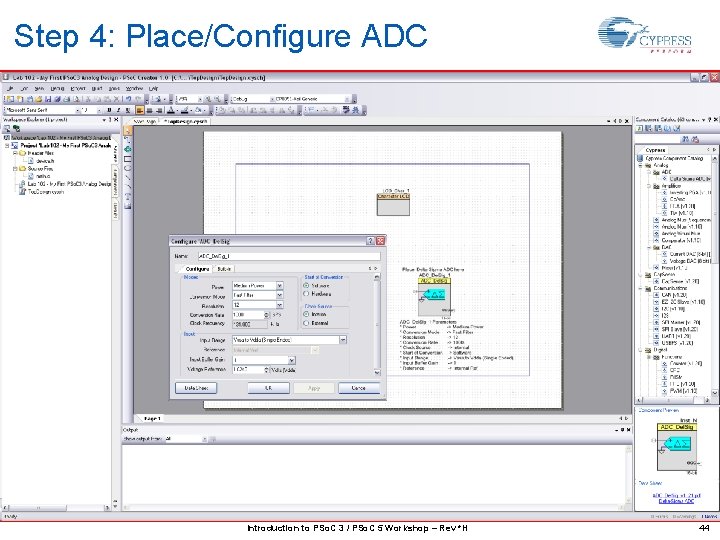
Step 4: Place/Configure ADC Introduction to PSo. C 3 / PSo. C 5 Workshop – Rev *H 44

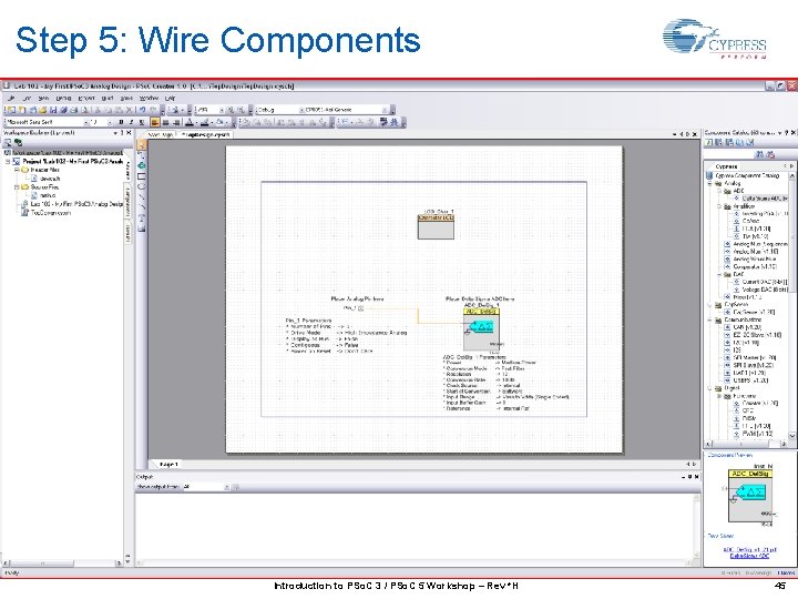
Step 5: Wire Components Introduction to PSo. C 3 / PSo. C 5 Workshop – Rev *H 45

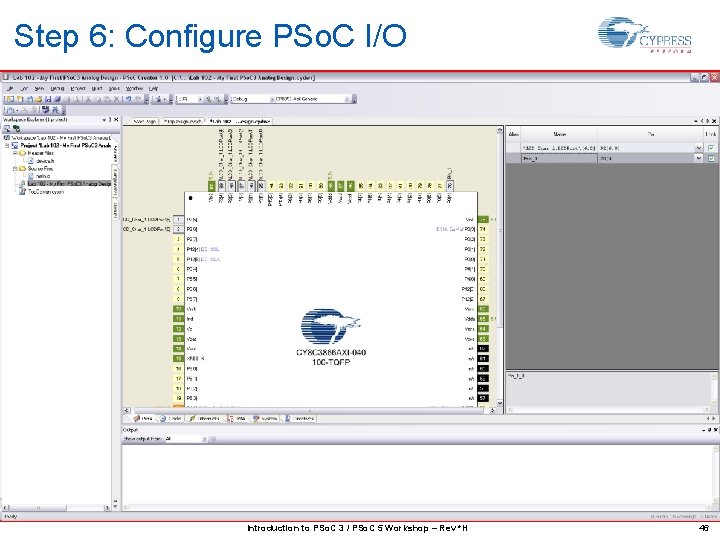
Step 6: Configure PSo. C I/O Introduction to PSo. C 3 / PSo. C 5 Workshop – Rev *H 46

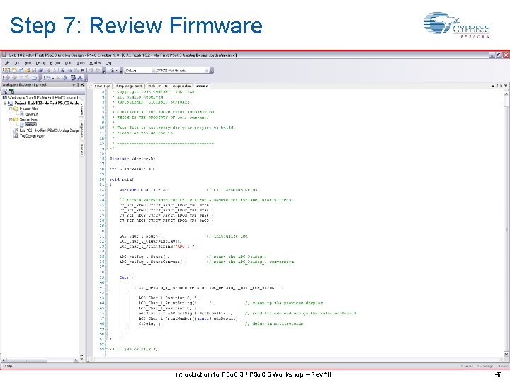
Step 7: Review Firmware Introduction to PSo. C 3 / PSo. C 5 Workshop – Rev *H 47

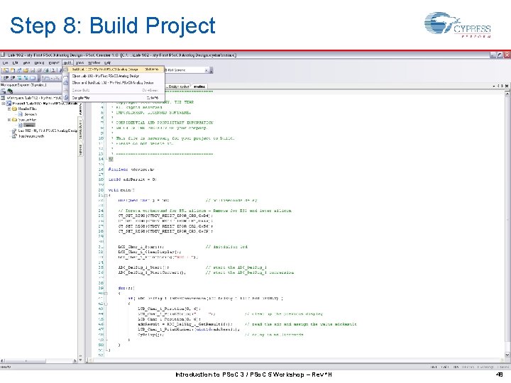
Step 8: Build Project Introduction to PSo. C 3 / PSo. C 5 Workshop – Rev *H 48

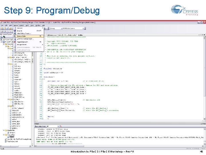
Step 9: Program/Debug Introduction to PSo. C 3 / PSo. C 5 Workshop – Rev *H 49

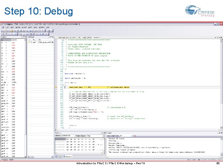
Step 10: Debug Introduction to PSo. C 3 / PSo. C 5 Workshop – Rev *H 50