Protection layer test device Fred Hartjes NIKHEF Protection
- Slides: 7

Protection layer test device Fred Hartjes NIKHEF Protection layer meeting Nikhef Dec 4, 2015

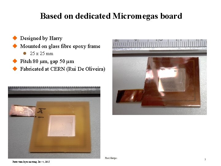
Based on dedicated Micromegas board u Designed by Harry u Mounted on glass fibre epoxy frame l 25 x 25 mm u Pitch 80 µm, gap 50 µm u Fabricated at CERN (Rui De Oliveira) Fred Hartjes Protection layer meeting. Dec 4, 2015 2

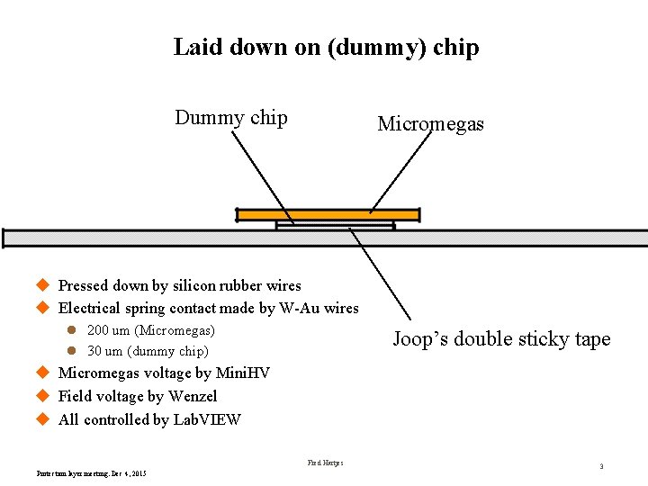
Laid down on (dummy) chip Dummy chip Micromegas u Pressed down by silicon rubber wires u Electrical spring contact made by W-Au wires l 200 um (Micromegas) l 30 um (dummy chip) Joop’s double sticky tape u Micromegas voltage by Mini. HV u Field voltage by Wenzel u All controlled by Lab. VIEW Fred Hartjes Protection layer meeting. Dec 4, 2015 3

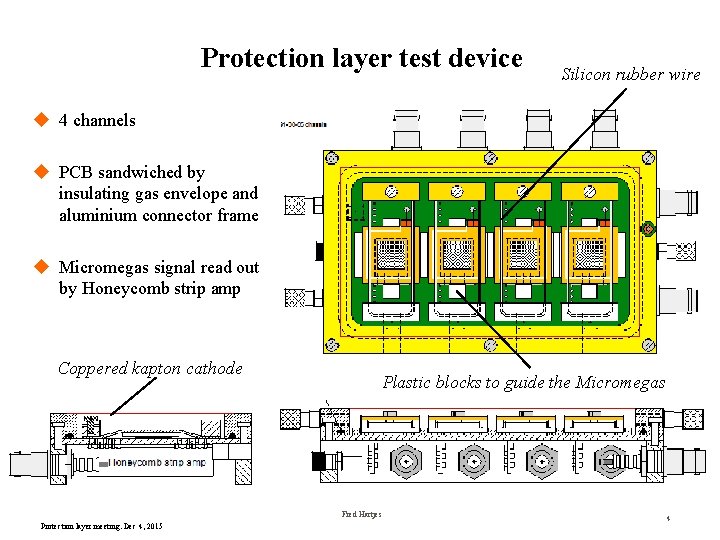
Protection layer test device Silicon rubber wire u 4 channels u PCB sandwiched by insulating gas envelope and aluminium connector frame u Micromegas signal read out by Honeycomb strip amp Coppered kapton cathode Plastic blocks to guide the Micromegas Fred Hartjes Protection layer meeting. Dec 4, 2015 4

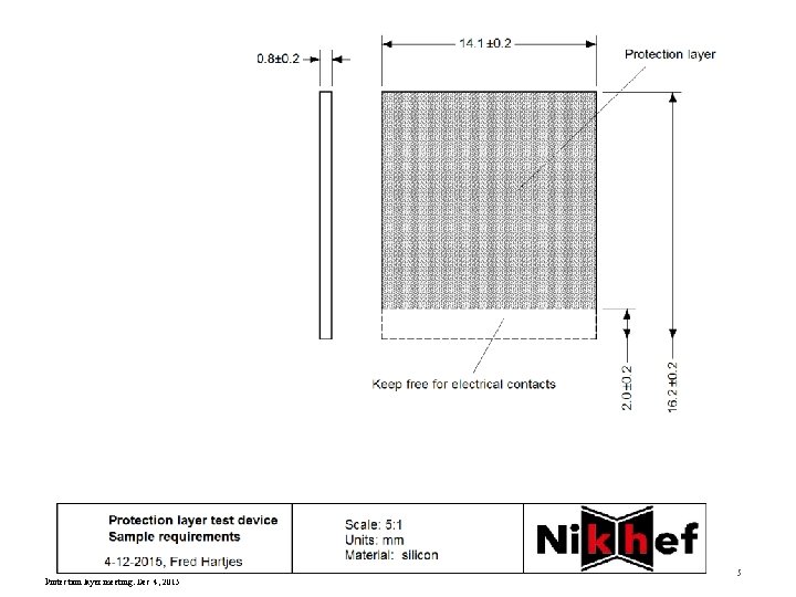
Fred Hartjes Protection layer meeting. Dec 4, 2015 5

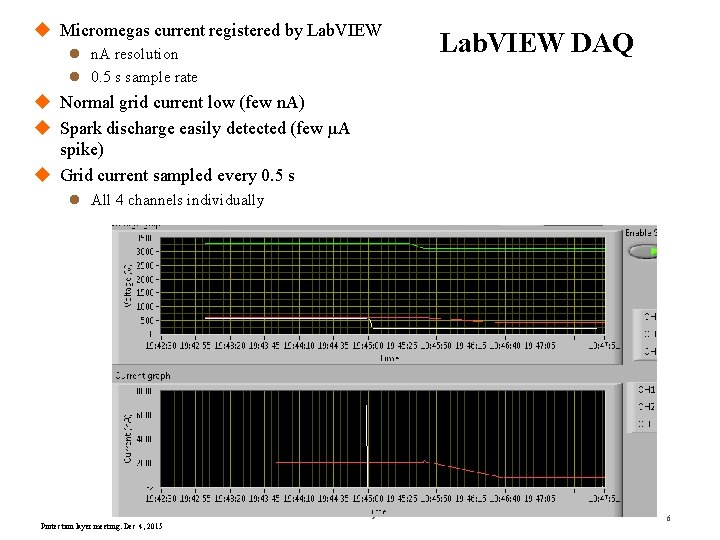
u Micromegas current registered by Lab. VIEW l n. A resolution l 0. 5 s sample rate Lab. VIEW DAQ u Normal grid current low (few n. A) u Spark discharge easily detected (few µA spike) u Grid current sampled every 0. 5 s l All 4 channels individually Fred Hartjes Protection layer meeting. Dec 4, 2015 6

Properties and prospects u New samples can be rapidly installed l Gas frame easily removed (only gas connections with quick couplings) l Spring contacts (W-Au wire) on sample and Micromegas l No gluing, wire bonding or soldering required u Rather small gas volume (~85 ml) u Irradiation with sources (90 Sr and 55 Fe) well possible u Analog RO of grid signal possible l Gain measurements using 55 Fe u In production l Parts (mechanics + PCB) expected mid January 2016 Fred Hartjes Protection layer meeting. Dec 4, 2015 7