PROPRIETARY NOTE THIS SPECIFICATION IS THE PROPERTY OF
- Slides: 26

PROPRIETARY NOTE THIS SPECIFICATION IS THE PROPERTY OF BOE HF AND SHALL NOT BE REPRODUCED OR COPIED WITHOUT THE WRITTEN PERMISSION OF BOE HF AND MUST BE RETURNED TO BOE HF UPON ITS REQUEST SPEC. NUMBER PRODUCT GROUP Rev. P 0 TFT-LCD ISSUE DATE PAGE 1 OF 31 TITLE : BP 101 WX 1 -600 Product Specification Rev. P 0 HEFEI BOE OPTOELECTRONICS TECHNOLOGY R 2010 -6053 -O(1/3) A 4(210 X 297)

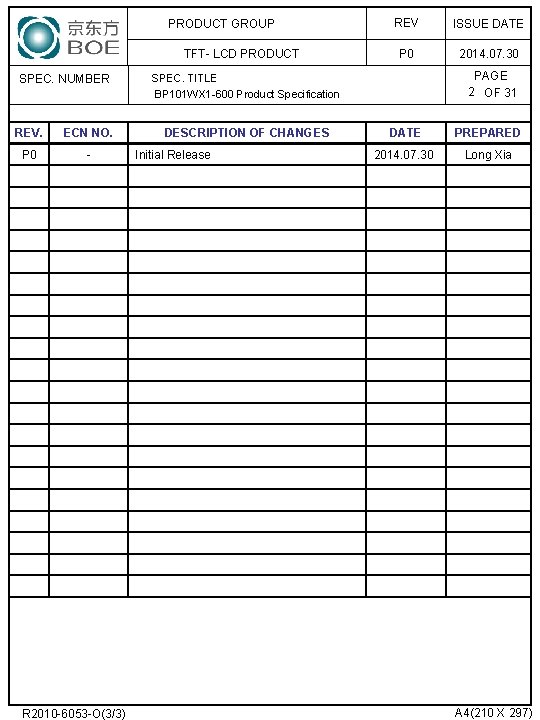
PRODUCT GROUP TFT- LCD PRODUCT SPEC. NUMBER REV. ECN NO. P 0 - R 2010 -6053 -O(3/3) REV ISSUE DATE P 0 2014. 07. 30 PAGE 2 OF 31 SPEC. TITLE BP 101 WX 1 -600 Product Specification DESCRIPTION OF CHANGES Initial Release DATE PREPARED 2014. 07. 30 Long Xia A 4(210 X 297)

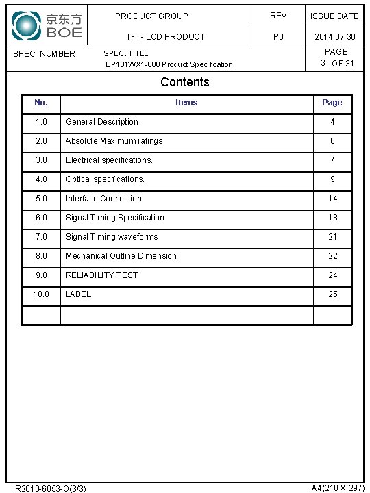
PRODUCT GROUP TFT- LCD PRODUCT SPEC. NUMBER SPEC. TITLE BP 101 WX 1 -600 Product Specification REV ISSUE DATE P 0 2014. 07. 30 PAGE 3 OF 31 Contents No. Items Page 1. 0 General Description 4 2. 0 Absolute Maximum ratings 6 3. 0 Electrical specifications. 7 4. 0 Optical specifications. 9 5. 0 Interface Connection 14 6. 0 Signal Timing Specification 18 7. 0 Signal Timing waveforms 21 8. 0 Mechanical Outline Dimension 22 9. 0 RELIABILITY TEST 24 10. 0 LABEL 25 R 2010 -6053 -O(3/3) A 4(210 X 297)

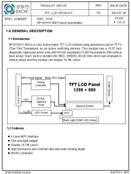
PRODUCT GROUP TFT- LCD PRODUCT SPEC. NUMBER REV ISSUE DATE P 0 2014. 07. 30 PAGE 4 OF 31 SPEC. TITLE BP 101 WX 1 -600 Product Specification 1. 0 GENERAL DESCRIPTION 1. 1 Introduction BP 101 WX 1 -600 is a color active matrix TFT LCD module using amorphous silicon TFT's (Thin Film Transistors) as an active switching devices. This module has a 10. 07 inch diagonally measured active area with WXGA resolutions (1280 horizontal by 800 vertical pixel array). Each pixel is divided into RED, GREEN, BLUE dots which are arranged in vertical stripe and this module can display 16. 7 M colors. MIPI Input Signal Mini. LVDS Signal VDD V_LED TFT LCD Panel 1280 × 800 DC/DC Gamma Vcom LED Driver Gate Driver Connector (CN 1) Timing Controller Source Driver FPC Back Light (SMD LED Array) 1. 2 Features 4 Lane MIPI Interface Thin and light weight Display 16. 7 M colors High luminance and contrast ratio and wide viewing angle Ro. HS Compliant R 2010 -6053 -O(3/3) A 4(210 X 297)

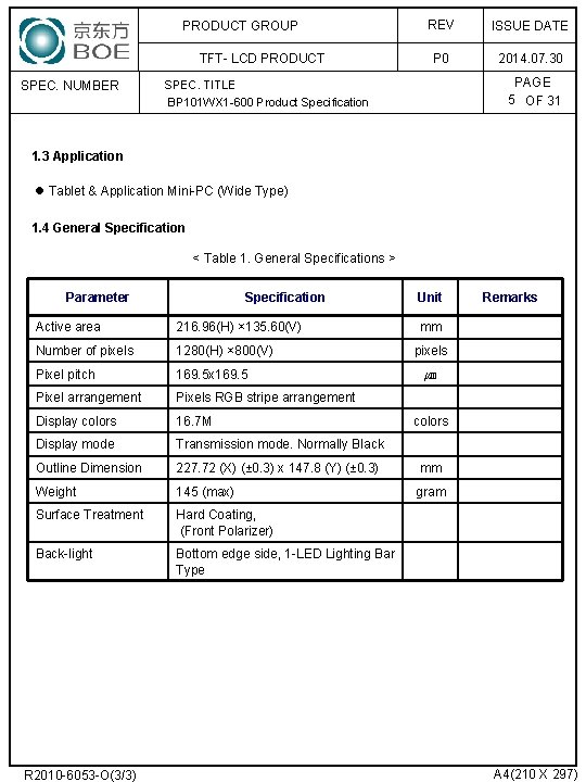
PRODUCT GROUP TFT- LCD PRODUCT SPEC. NUMBER REV ISSUE DATE P 0 2014. 07. 30 PAGE 5 OF 31 SPEC. TITLE BP 101 WX 1 -600 Product Specification 1. 3 Application Tablet & Application Mini-PC (Wide Type) 1. 4 General Specification < Table 1. General Specifications > Parameter Specification Active area 216. 96(H) × 135. 60(V) Number of pixels 1280(H) × 800(V) Pixel pitch 169. 5 x 169. 5 Pixel arrangement Pixels RGB stripe arrangement Display colors 16. 7 M Display mode Transmission mode. Normally Black Outline Dimension 227. 72 (X) (± 0. 3) x 147. 8 (Y) (± 0. 3) Weight 145 (max) Surface Treatment Hard Coating, (Front Polarizer) Back-light Bottom edge side, 1 -LED Lighting Bar Type R 2010 -6053 -O(3/3) Unit Remarks mm pixels ㎛ colors mm gram A 4(210 X 297)

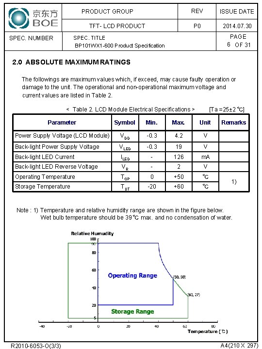
PRODUCT GROUP TFT- LCD PRODUCT SPEC. NUMBER REV ISSUE DATE P 0 2014. 07. 30 PAGE 6 OF 31 SPEC. TITLE BP 101 WX 1 -600 Product Specification 2. 0 ABSOLUTE MAXIMUM RATINGS The followings are maximum values which, if exceed, may cause faulty operation or damage to the unit. The operational and non-operational maximum voltage and current values are listed in Table 2. < Table 2. LCD Module Electrical Specifications > [Ta =25± 2 ℃] Parameter Symbol Min. Max. Unit Power Supply Voltage (LCD Module) VDD -0. 3 4. 2 V Back-light Power Supply Voltage VLED -0. 3 19 V Back-light LED Current ILED - 126 m. A Back-light LED Reverse Voltage VR - 2 V Operating Temperature TOP 0 +50 ℃ Storage Temperature TST -20 +60 ℃ Remarks 1) Note : 1) Temperature and relative humidity range are shown in the figure below. Wet bulb temperature should be 39 ℃ max. and no condensation of water. R 2010 -6053 -O(3/3) A 4(210 X 297)

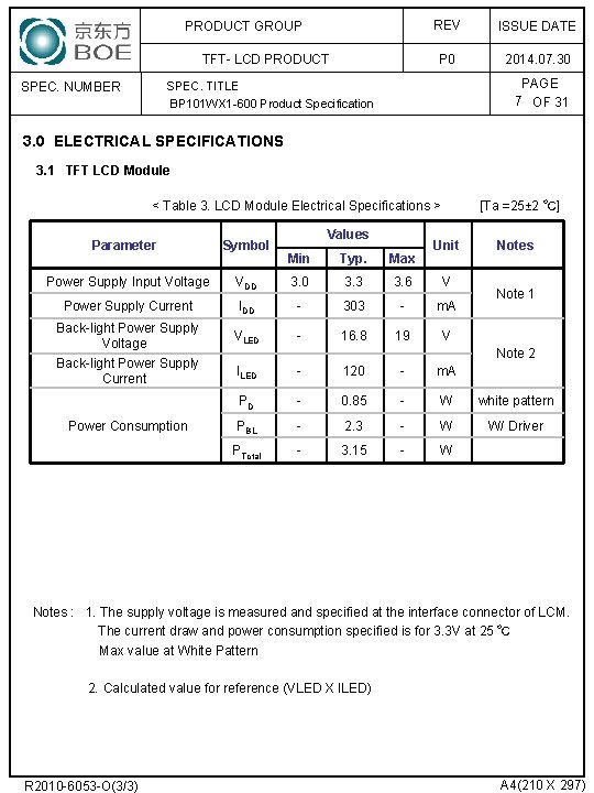
PRODUCT GROUP TFT- LCD PRODUCT SPEC. NUMBER REV ISSUE DATE P 0 2014. 07. 30 PAGE 7 OF 31 SPEC. TITLE BP 101 WX 1 -600 Product Specification 3. 0 ELECTRICAL SPECIFICATIONS 3. 1 TFT LCD Module < Table 3. LCD Module Electrical Specifications > Parameter Symbol Power Supply Input Voltage Power Supply Current Back-light Power Supply Voltage Back-light Power Supply Current Power Consumption Values [Ta =25± 2 ℃] Unit Min Typ. Max VDD 3. 0 3. 3 3. 6 V IDD - 303 - m. A VLED - 16. 8 19 V Notes Note 1 Note 2 ILED - 120 - m. A PD - 0. 85 - W white pattern PBL - 2. 3 - W W/ Driver PTotal - 3. 15 - W Notes : 1. The supply voltage is measured and specified at the interface connector of LCM. The current draw and power consumption specified is for 3. 3 V at 25 ℃ Max value at White Pattern 2. Calculated value for reference (VLED X ILED) R 2010 -6053 -O(3/3) A 4(210 X 297)

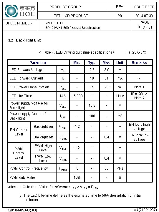
PRODUCT GROUP TFT- LCD PRODUCT SPEC. NUMBER REV ISSUE DATE P 0 2014. 07. 30 PAGE 8 OF 31 SPEC. TITLE BP 101 WX 1 -600 Product Specification 3. 2 Back-light Unit < Table 4. LED Driving guideline specifications > Parameter Ta=25+/-2°C Min. Typ. Max. Unit Remarks LED Forward Voltage VF - 2. 8 3. 0 V - LED Forward Current IF - 18 21 m. A - LED Power Consumption PLED - 2 2. 3 W Note 1 LED Life-Time N/A 15, 000 - - Hour IF = 20 m. A Note 2 Power supply voltage for Back light VLED - 16. 8 - V Power supply Current for Back light ILED - 108 - m. A Backlight on VENH 1. 2 - - V EN logic high voltage Backlight off VENL - - 0. 4 V EN logic low voltage PWM High Level VPML 1. 2 - - V PWM Low Level VPML - - 0. 4 V FPWM 5 - 20 KHz 10% - - % EN Control Level PWM Control Frequency PWM duty Ratio Notes : 1. Calculator Value for reference ILED × VLED = PLED 2. The LED Life-time define as the estimated time to 50% degradation of initial luminous. R 2010 -6053 -O(3/3) A 4(210 X 297)

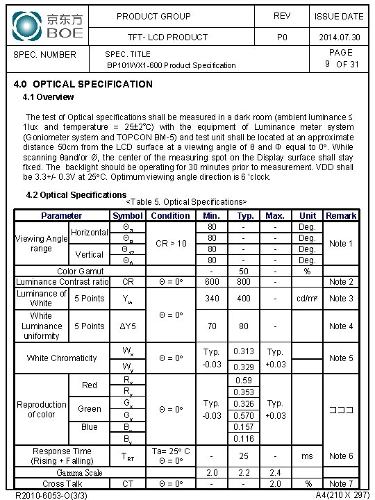
PRODUCT GROUP REV ISSUE DATE P 0 2014. 07. 30 TFT- LCD PRODUCT SPEC. NUMBER PAGE 9 OF 31 SPEC. TITLE BP 101 WX 1 -600 Product Specification 4. 0 OPTICAL SPECIFICATION 4. 1 Overview The test of Optical specifications shall be measured in a dark room (ambient luminance 1 lux and temperature = 25 2℃) with the equipment of Luminance meter system (Goniometer system and TOPCON BM-5) and test unit shall be located at an approximate distance 50 cm from the LCD surface at a viewing angle of θ and Φ equal to 0. While scanning θand/or Ø, the center of the measuring spot on the Display surface shall stay fixed. The backlight should be operating for 30 minutes prior to measurement. VDD shall be 3. 3+/- 0. 3 V at 25 C. Optimum viewing angle direction is 6 ’clock. 4. 2 Optical Specifications <Table 5. Optical Specifications> Parameter Symbol Θ 3 Horizontal Θ 9 Viewing Angle range Θ 12 Vertical Θ 6 Color Gamut Luminance Contrast ratio CR Luminance of 5 Points Yw White ΔY 5 Luminance 5 Points uniformity White Chromaticity Red Reproduction of color Green Blue Response Time (Rising + Falling) Gamma Scale Cross Talk R 2010 -6053 -O(3/3) Wx Wy Condition CR > 10 Θ = 0 Min. 80 80 600 Typ. 50 800 Max. - Unit Deg. % Remark 340 400 - cd/m 2 70 80 - Note 4 Typ. -0. 03 0. 313 Typ. +0. 03 Note 5 Typ. +0. 03 ��� Note 1 Note 2 Note 3 Θ = 0 0. 329 Rx Ry Gx Gy Bx By Θ = 0 Typ. -0. 03 0. 59 0. 353 0. 326 0. 570 0. 157 0. 116 TRT Ta= 25 C Θ = 0 - 25 - ms Note 6 2. 0 - 2. 2 - 2. 4 2. 0 % Note 7 A 4(210 X 297) CT Θ = 0

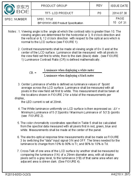
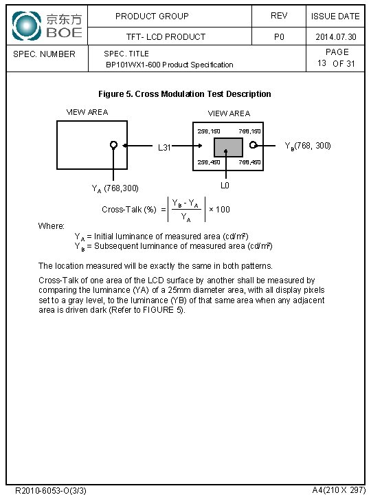
PRODUCT GROUP TFT- LCD PRODUCT SPEC. NUMBER SPEC. TITLE BP 101 WX 1 -600 Product Specification REV ISSUE DATE P 0 2014. 07. 30 PAGE 10 OF 31 Notes : 1. Viewing angle is the angle at which the contrast ratio is greater than 10. The viewing angles are determined for the horizontal or 3, 9 o’clock direction and the vertical or 6, 12 o’clock direction with respect to the optical axis which is normal to the LCD surface (see FIGURE 1). 2. Contrast measurements shall be made at viewing angle of Θ= 0 and at the center of the LCD surface. Luminance shall be measured with all pixels in the view field set first to white, then to the dark (black) state. (see FIGURE 1) Luminance Contrast Ratio (CR) is defined mathematically. CR = Luminance when displaying a white raster Luminance when displaying a black raster 3. Center Luminance of white is defined as luminance values of 5 point average across the LCD surface. Luminance shall be measured with all pixels in the view field set first to white. This measurement shall be taken at the locations shown in FIGURE 2 for a total of the measurements per display, the LED current is set at 20 m. A. 4. The White luminance uniformity on LCD surface is then expressed as : ΔY = Minimum Luminance of 5 (13)points / Maximum Luminance of 5(13) (points (see FIGURE 2). 5. The color chromaticity coordinates specified in Table 5 shall be calculated from the spectral data measured with all pixels first in red, green, blue and white. Measurements shall be made at the center of the panel. 6. The electro-optical response time measurements shall be made as FIGURE 3 by switching the “data” input signal ON and OFF. The times needed for the luminance to change from 10% to 90% is Tr, and 90% to 10% is Td. 7. Cross-Talk of one area of the LCD surface by another shall be measured by comparing the luminance (YA) of a 25 mm diameter area, with all display pixels set to a gray level, to the luminance (YB) of that same area when any adjacent area is driven dark. (See FIGURE 4). R 2010 -6053 -O(3/3) A 4(210 X 297)

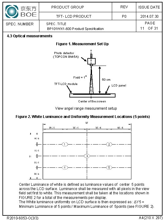
PRODUCT GROUP TFT- LCD PRODUCT SPEC. NUMBER REV ISSUE DATE P 0 2014. 07. 30 PAGE 11 OF 31 SPEC. TITLE BP 101 WX 1 -600 Product Specification 4. 3 Optical measurements Figure 1. Measurement Set Up Photo detector (TOPCON BM-5 A) o Field = 1 50 cm TFT-LCD module LCD panel Center of the screen View angel range measurement setup Figure 2. White Luminance and Uniformity Measurement Locations (5 points) Center Luminance of white is defined as luminance values of center 5 points across the LCD surface. Luminance shall be measured with all pixels in the view field set first to white. This measurement shall be taken at the locations shown in FIGURE 2 for a total of the measurements per display. The White luminance uniformity on LCD surface is then expressed as : ΔY 5 = Minimum Luminance of 5 points / Maximum Luminance of 5 points (see FIGURE 2). R 2010 -6053 -O(3/3) A 4(210 X 297)

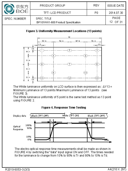
PRODUCT GROUP TFT- LCD PRODUCT SPEC. NUMBER REV ISSUE DATE P 0 2014. 07. 30 PAGE 12 OF 31 SPEC. TITLE BP 101 WX 1 -600 Product Specification Figure 3. Uniformity Measurement Locations (13 points) The White luminance uniformity on LCD surface is then expressed as : ΔY 13 = Minimum Luminance of 13 points /Maximum Luminance of 13 points (see FIGURE 3). The White luminance uniformity of 5 point is the same test method as 13 point using FIGURE 2. Figure 4. Response Time Testing Display data White (TFT ON) Black (TFT OFF) TR Optical Response 100% 90% 10% 0% Black (TFT OFF) TF Time The electro-optical response time measurements shall be made as shown in FIGURE 4 by switching the “data” input signal ON and OFF. The times needed for the luminance to change from 10% to 90% is Tr and 90% to 10% is Td. R 2010 -6053 -O(3/3) A 4(210 X 297)

PRODUCT GROUP REV ISSUE DATE P 0 2014. 07. 30 TFT- LCD PRODUCT SPEC. NUMBER PAGE 13 OF 31 SPEC. TITLE BP 101 WX 1 -600 Product Specification Figure 5. Cross Modulation Test Description VIEW AREA 256, 150 768, 150 YB(768, 300) L 31 256, 450 L 0 YA (768, 300) Cross-Talk (%) = Where: 768, 450 YB - Y A YA × 100 Y A = Initial luminance of measured area (cd/m 2) Y B = Subsequent luminance of measured area (cd/m 2) The location measured will be exactly the same in both patterns. Cross-Talk of one area of the LCD surface by another shall be measured by comparing the luminance (YA) of a 25 mm diameter area, with all display pixels set to a gray level, to the luminance (YB) of that same area when any adjacent area is driven dark (Refer to FIGURE 5). R 2010 -6053 -O(3/3) A 4(210 X 297)

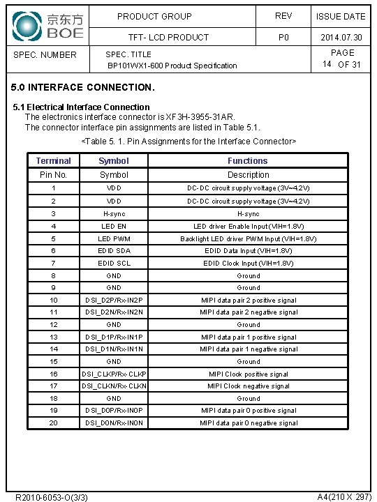
PRODUCT GROUP TFT- LCD PRODUCT SPEC. NUMBER REV ISSUE DATE P 0 2014. 07. 30 SPEC. TITLE BP 101 WX 1 -600 Product Specification PAGE 14 OF 31 5. 0 INTERFACE CONNECTION. 5. 1 Electrical Interface Connection The electronics interface connector is XF 3 H-3955 -31 AR. The connector interface pin assignments are listed in Table 5. 1. <Table 5. 1. Pin Assignments for the Interface Connector> Terminal Symbol Functions Pin No. Symbol Description 1 VDD DC-DC circuit supply voltage (3 V~4. 2 V) 2 VDD DC-DC circuit supply voltage (3 V~4. 2 V) 3 H-sync 4 LED EN LED driver Enable Input (VIH=1. 8 V) 5 LED PWM Backlight LED driver PWM Input (VIH=1. 8 V) 6 EDID SDA EDID Data Input (VIH=1. 8 V) 7 EDID SCL EDID Clock Input (VIH=1. 8 V) 8 GND Ground 9 GND Ground 10 DSI_D 2 P/Rx-IN 2 P MIPI data pair 2 positive signal 11 DSI_D 2 N/Rx-IN 2 N MIPI data pair 2 negative signal 12 GND Ground 13 DSI_D 1 P/Rx-IN 1 P MIPI data pair 1 positive signal 14 DSI_D 1 N/Rx-IN 1 N MIPI data pair 1 negative signal 15 GND Ground 16 DSI_CLKP/Rx-CLKP MIPI Clock positive signal 17 DSI_CLKN/Rx-CLKN MIPI Clock negative signal 18 GND Ground 19 DSI_D 0 P/Rx-IN 0 P MIPI data pair 0 positive signal 20 DSI_D 0 N/Rx-IN 0 N MIPI data pair 0 negative signal R 2010 -6053 -O(3/3) A 4(210 X 297)

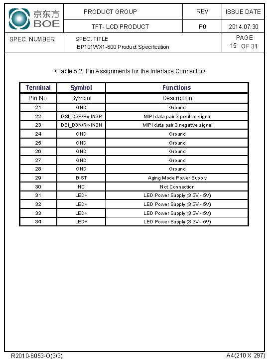
PRODUCT GROUP TFT- LCD PRODUCT SPEC. NUMBER REV ISSUE DATE P 0 2014. 07. 30 SPEC. TITLE BP 101 WX 1 -600 Product Specification PAGE 15 OF 31 <Table 5. 2. Pin Assignments for the Interface Connector> Terminal Symbol Functions Pin No. Symbol Description 21 GND Ground 22 DSI_D 3 P/Rx-IN 3 P MIPI data pair 3 positive signal 23 DSI_D 3 N/Rx-IN 3 N MIPI data pair 3 negative signal 24 GND Ground 25 GND Ground 26 GND Ground 27 GND Ground 28 GND Ground 29 BIST Aging Mode Power Supply 30 NC Not Connection 31 LED+ LED Power Supply (3. 3 V - 5 V) 32 LED+ LED Power Supply (3. 3 V - 5 V) 33 LED+ LED Power Supply (3. 3 V - 5 V) 34 LED+ LED Power Supply (3. 3 V - 5 V) R 2010 -6053 -O(3/3) A 4(210 X 297)

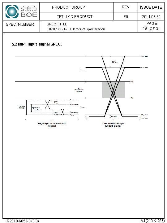
PRODUCT GROUP TFT- LCD PRODUCT SPEC. NUMBER SPEC. TITLE BP 101 WX 1 -600 Product Specification REV ISSUE DATE P 0 2014. 07. 30 PAGE 16 OF 31 5. 2 MIPI Input signal SPEC. R 2010 -6053 -O(3/3) A 4(210 X 297)

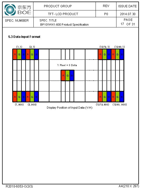
PRODUCT GROUP TFT- LCD PRODUCT SPEC. NUMBER REV ISSUE DATE P 0 2014. 07. 30 PAGE 17 OF 31 SPEC. TITLE BP 101 WX 1 -600 Product Specification 5. 3 Data Input Format (1, 1) (2, 1) (1279, 1) R G B (1280, 1) R G B 1 Pixel = 3 Dots R G B (1, 800) R G B (2, 800) (1279, 800) (1280, 800) Display Position of Input Data (V-H) R 2010 -6053 -O(3/3) A 4(210 X 297)

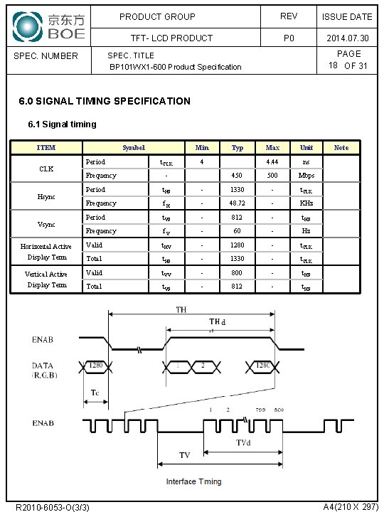
PRODUCT GROUP TFT- LCD PRODUCT SPEC. NUMBER REV ISSUE DATE P 0 2014. 07. 30 PAGE 18 OF 31 SPEC. TITLE BP 101 WX 1 -600 Product Specification 6. 0 SIGNAL TIMING SPECIFICATION 6. 1 Signal timing ITEM CLK Symbol Period Frequency Min t. CLK Typ Max Unit 4. 44 ns 450 500 Mbps 4 - Period t. HP - 1330 - t. CLK Frequency f. H - 48. 72 - KHz Period t. VP - 812 - t. HP Frequency f. V - 60 - Hz Horizontal Active Display Term Valid t. HV - 1280 - t. CLK Total t. HP - 1330 - t. CLK Vertical Active Display Term Valid t. VV - 800 - t. HP Total t. VP - 812 - t. HP Hsync Vsync R 2010 -6053 -O(3/3) Note A 4(210 X 297)

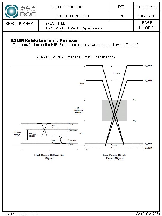
PRODUCT GROUP TFT- LCD PRODUCT SPEC. NUMBER SPEC. TITLE BP 101 WX 1 -600 Product Specification REV ISSUE DATE P 0 2014. 07. 30 PAGE 19 OF 31 6. 2 MIPI Rx Interface Timing Parameter The specification of the MIPI Rx interface timing parameter is shown in Table 6. <Table 6. MIPI Rx Interface Timing Specification> R 2010 -6053 -O(3/3) A 4(210 X 297)

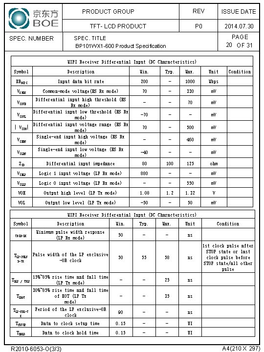
PRODUCT GROUP REV ISSUE DATE P 0 2014. 07. 30 TFT- LCD PRODUCT SPEC. NUMBER PAGE 20 OF 31 SPEC. TITLE BP 101 WX 1 -600 Product Specification MIPI Receiver Differential Input (DC Characteristics) Symbol Description Min. Typ. Max. Unit BRMIPI Input data bit rate 200 - 1000 Mbps VCMRX Common-mode voltage(HS Rx mode) 70 - 330 m. V - - 70 m. V -70 - - m. V 70 - 500 m. V - - 460 m. V -40 - - m. V Differential input high threshold (HS Rx mode) Differential input low threshold (HS Rx VIDTL mode) Differential input voltage range (HS Rx | VIDM| mode) Single-end input high voltage (HS Rx VIHHS mode) Single-end input low voltage (HS Rx VILHS mode) VIDTH ZID Differential input impedance 80 100 125 ohm VIHLP Logic 1 input voltage (LP Rx mode) 880 - - m. V VILLP Logic 0 input voltage (LP Rx mode) - - 550 m. V VOH Output high level (LP Tx mode) 1. 08 1. 2 1. 32 V VOL Output low level (LP Tx mode) -50 - 50 m. V Condition MIPI Receiver Differential Input (DC Characteristics) Symbol Description Min. Typ. Max. Unit TMIN-RX Minimum pulse width response (LP Rx mode) 50 - - ns TLP-PULS Pulse width of the LP exclusive -OR clock E-TX 50 55 58 ns - - 25 ns - - 35 ns 90 - - ns X 15%~85% rise time and fall time (LP Tx mode) 30%~85% rise time and fall time of EOT (LP Tx mode) Period of the LP exclusive-OR clock TSETUP Data to clock setup time 0. 15 - - UI THOLD Data to clock hold time 0. 15 - - UI TRLP / TFLP TREOT TLP-PER-T R 2010 -6053 -O(3/3) Condition 1 st clock pulse after STOP state or last clock pulse before STOP state/all other pulse A 4(210 X 297)

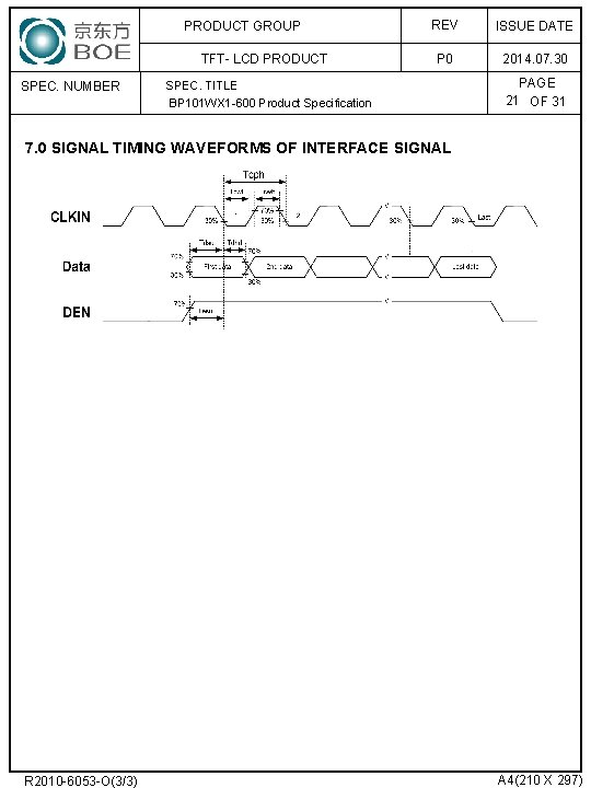
PRODUCT GROUP TFT- LCD PRODUCT SPEC. NUMBER REV ISSUE DATE P 0 2014. 07. 30 SPEC. TITLE BP 101 WX 1 -600 Product Specification PAGE 21 OF 31 7. 0 SIGNAL TIMING WAVEFORMS OF INTERFACE SIGNAL R 2010 -6053 -O(3/3) A 4(210 X 297)

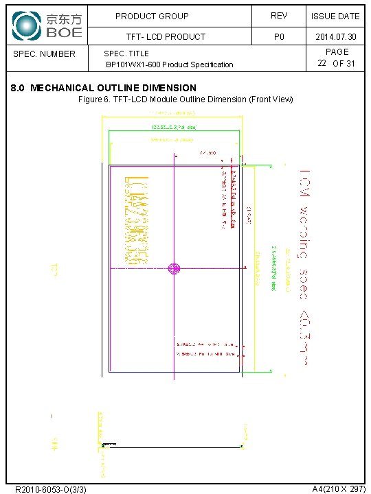
PRODUCT GROUP TFT- LCD PRODUCT SPEC. NUMBER REV ISSUE DATE P 0 2014. 07. 30 SPEC. TITLE BP 101 WX 1 -600 Product Specification PAGE 22 OF 31 8. 0 MECHANICAL OUTLINE DIMENSION Figure 6. TFT-LCD Module Outline Dimension (Front View) R 2010 -6053 -O(3/3) A 4(210 X 297)

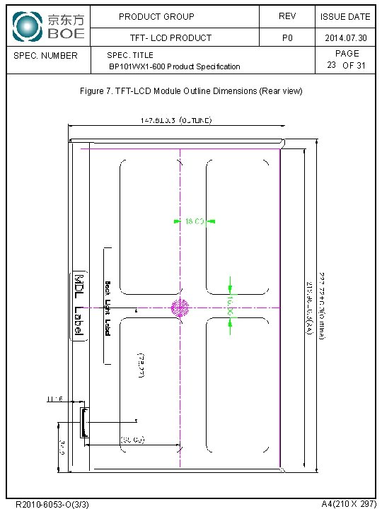
PRODUCT GROUP TFT- LCD PRODUCT SPEC. NUMBER REV ISSUE DATE P 0 2014. 07. 30 SPEC. TITLE BP 101 WX 1 -600 Product Specification PAGE 23 OF 31 Figure 7. TFT-LCD Module Outline Dimensions (Rear view) R 2010 -6053 -O(3/3) A 4(210 X 297)

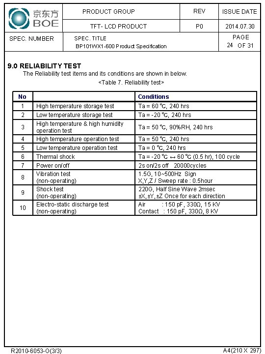
PRODUCT GROUP TFT- LCD PRODUCT SPEC. NUMBER REV ISSUE DATE P 0 2014. 07. 30 PAGE 24 OF 31 SPEC. TITLE BP 101 WX 1 -600 Product Specification 9. 0 RELIABILITY TEST The Reliability test items and its conditions are shown in below. <Table 7. Reliability test> No Conditions 1 High temperature storage test Ta = 60 ℃, 240 hrs 2 Ta = -20 ℃, 240 hrs 4 5 Low temperature storage test High temperature & high humidity operation test High temperature operation test Low temperature operation test 6 Thermal shock Ta = -20 ℃ ↔ 60 ℃ (0. 5 hr), 100 cycle 7 Power on/off Vibration test (non-operating) Shock test (non-operating) Electro-static discharge test (non-operating) 2 s on/2 s off 20000 cycles 1. 5 G, 10~500 Hz Sign X, Y, Z / Sweep rate : 0. 5 hour 220 G, Half Sine Wave 2 msec ±X, ±Y, ±Z Once for each direction Air : 150 p. F, 330Ω, 15 KV Contact : 150 p. F, 330Ω, 8 KV 3 8 9 10 R 2010 -6053 -O(3/3) Ta = 50 ℃, 90%RH, 240 hrs Ta = 50 ℃, 240 hrs Ta = 0 ℃, 240 hrs A 4(210 X 297)

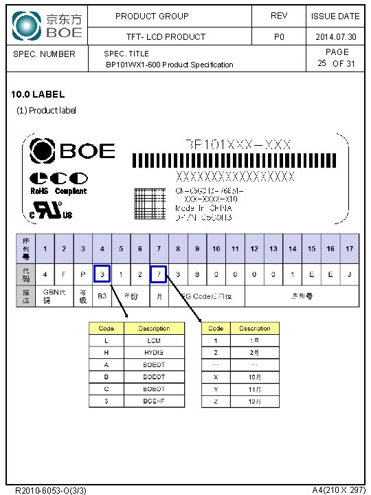
PRODUCT GROUP TFT- LCD PRODUCT SPEC. NUMBER SPEC. TITLE BP 101 WX 1 -600 Product Specification REV ISSUE DATE P 0 2014. 07. 30 PAGE 25 OF 31 10. 0 LABEL (1) Product label R 2010 -6053 -O(3/3) A 4(210 X 297)

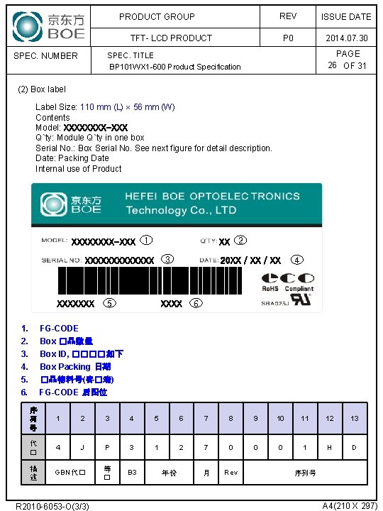
PRODUCT GROUP REV ISSUE DATE P 0 2014. 07. 30 TFT- LCD PRODUCT SPEC. NUMBER PAGE 26 OF 31 SPEC. TITLE BP 101 WX 1 -600 Product Specification (2) Box label Label Size: 110 mm (L) 56 mm (W) Contents Model: XXXX-XXX Q`ty: Module Q`ty in one box Serial No. : Box Serial No. See next figure for detail description. Date: Packing Date Internal use of Product XXXX-XXX 1 XX 2 3 XXXXXXX 1. 2. 3. 4. 5. 6. 5 20 XX / XX XXXX 4 6 FG-CODE Box �品数量 Box ID, ����如下 Box Packing 日期 �品物料号(客�端) FG-CODE 后四位 序 列 号 1 2 3 4 5 6 7 8 9 10 11 12 13 代 � 4 J P 3 1 2 7 0 0 0 1 H D 描 述 GBN代� 等 � B 3 月 Rev R 2010 -6053 -O(3/3) 年份 序列号 A 4(210 X 297)