Properties of Sun Light Measurement of Solar Radiation
- Slides: 30

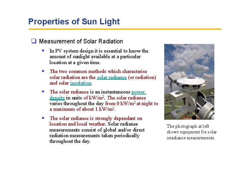
Properties of Sun Light Measurement of Solar Radiation In PV system design it is essential to know the amount of sunlight available at a particular location at a given time. The two common methods which characterise solar radiation are the solar radiance (or radiation) and solar insolation. The solar radiance is an instantaneous power density in units of k. W/m 2. The solar radiance varies throughout the day from 0 k. W/m 2 at night to a maximum of about 1 k. W/m 2. The solar radiance is strongly dependant on location and local weather. Solar radiance measurements consist of global and/or direct radiation measurements taken periodically throughout the day. The photograph at left shows equipment for solar irradiance measurements.

Properties of Sun Light Measurement of Solar Radiation While solar irradiance is most commonly measured, a more common form of radiation data used in system design is the solar insolation. The solar insolation is the total amount of solar energy received at a particular location during a specified time period, often in units of k. Wh/(m 2 day). While the units of solar insolation and solar irradiance are both a power density (for solar insolation the "hours" in the numerator are a time measurement as is the "day" in the denominator), solar insolation is quite different than the solar irradiance as the solar insolation is the instantaneous solar irradiance averaged over a given time period. Solar insolation can also be expressed in units of MJ/m 2 per year.

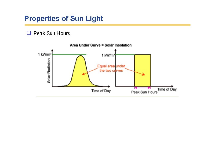
Properties of Sun Light Average Solar Radiation The average daily solar radiation at a location in a given month is often sufficient for a basic system analysis. This data may be presented either as measured on the horizontal or measured with the measuring surface perpendicular to the solar radiation. Peak Sun Hours The average daily solar insolation in units of k. Wh/m 2 per day is sometimes referred to as "peak sun hours". The term "peak sun hours" refers to the solar insolation which a particular location would receive if the sun were shining at its maximum value for a certain number of hours. Since the peak solar radiation is 1 k. W/m 2, the number of peak sun hours is numerically identical to the average daily solar insolation. For example, a location that receives 8 k. Wh/m 2 per day can be said to have received 8 hours of sun per day at 1 k. W/m 2.

Properties of Sun Light Peak Sun Hours

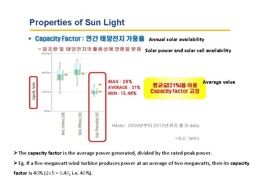
Properties of Sun Light Annual solar availability Solar power and solar cell availability Average value ØThe capacity factor is the average power generated, divided by the rated peak power. ØEg. If a five-megawatt wind turbine produces power at an average of two megawatts, then its capacity factor is 40% (2÷ 5 = 0. 40, i. e. 40%).

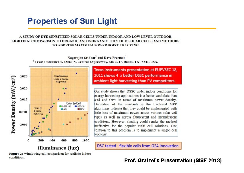
Properties of Sun Light Prof. Gratzel’s Presentation (SISF 2013)

Maximum power point tracking (MPPT) is an algorithm implemented in photovoltaic (PV) inverters to continuously adjust the impedance seen by the solar array to keep the PV system operating at, or close to, the peak power point of the PV panel under varying conditions, like changing solar irradiance, temperature, and load. Engineers developing solar inverters implement MPPT algorithms to maximize the power generated by PV systems. The algorithms control the voltage to ensure that the system operates at “maximum power point” (or peak voltage) on the power voltage curve, as shown below. MPPT algorithms are typically used in the controller designs for PV systems. The algorithms account for factors such as variable irradiance (sunlight) and temperature to ensure that the PV system generates maximum power at all times. Shading shading is a problem in PV modules since shading just one cell in the module can reduce the power output to zero. The cells in a module are all connected in series. Shading of a Single Cell The output of a cell declines when shaded by a tree branch, building or module dust. The output declines proportionally to the amount of shading. For completely opaque objects such as a leaf, the decline in current output of the cell is proportional to the amount of the cell that is obscured.

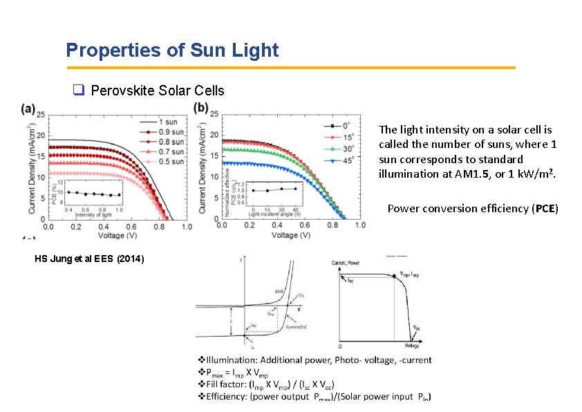
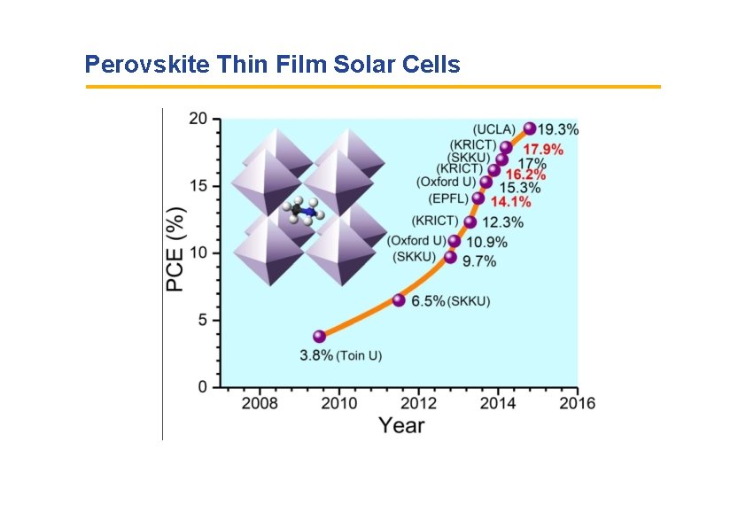
Properties of Sun Light Perovskite Solar Cells The light intensity on a solar cell is called the number of suns, where 1 sun corresponds to standard illumination at AM 1. 5, or 1 k. W/m 2. Power conversion efficiency (PCE) HS Jung et al EES (2014)

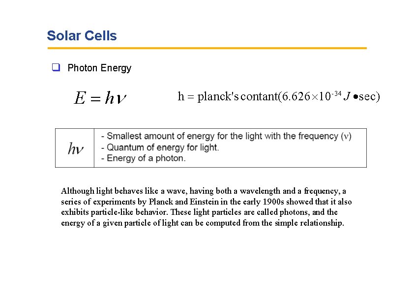
Solar Cells Photon Energy E h h planck's contant(6. 626 10 -34 J sec) Although light behaves like a wave, having both a wavelength and a frequency, a series of experiments by Planck and Einstein in the early 1900 s showed that it also exhibits particle-like behavior. These light particles are called photons, and the energy of a given particle of light can be computed from the simple relationship.

Solar Cells BASIC RESEARCH CHALLENGES FOR SOLAR ELECTRICITY Edmund Becquerel discovered the photovoltaic (PV) effect in 1839 Voltage and a current were produced when a silver chloride electrode immersed in an electrolytic solution and connected to a counter metal electrode was illuminated with white light The birth of the modern era of PV solar cells occurred in 1954, when D. Chapin, C. Fuller, and G. Pearson at Bell Labs demonstrated solar cells based on p-n junctions in single crystal Si with efficiencies of 5– 6% From the mid 1950 s to the early 1970 s, PV research and development (R&D) was directed primarily toward space applications and satellite power. In 1973, a greatly increased level of R&D on solar cells was initiated due to oil embargo

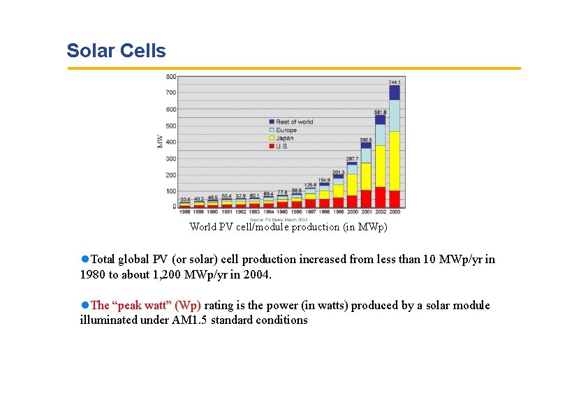
Solar Cells World PV cell/module production (in MWp) Total global PV (or solar) cell production increased from less than 10 MWp/yr in 1980 to about 1, 200 MWp/yr in 2004. The “peak watt” (Wp) rating is the power (in watts) produced by a solar module illuminated under AM 1. 5 standard conditions

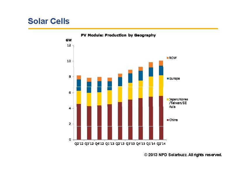
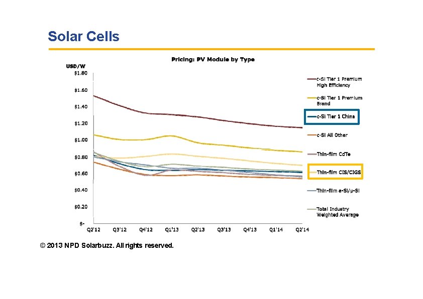
Solar Cells © 2013 NPD Solarbuzz. All rights reserved.

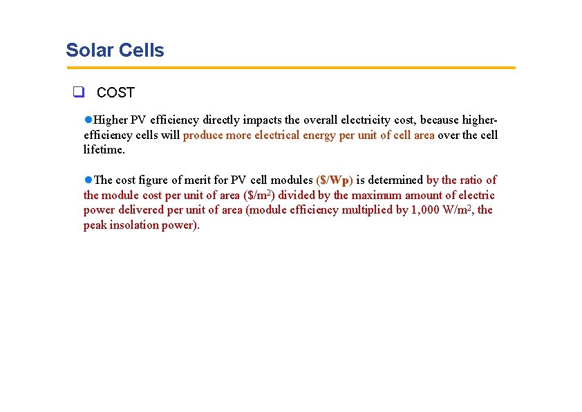
Solar Cells COST Higher PV efficiency directly impacts the overall electricity cost, because higherefficiency cells will produce more electrical energy per unit of cell area over the cell lifetime. The cost figure of merit for PV cell modules ($/Wp) is determined by the ratio of the module cost per unit of area ($/m 2) divided by the maximum amount of electric power delivered per unit of area (module efficiency multiplied by 1, 000 W/m 2, the peak insolation power).

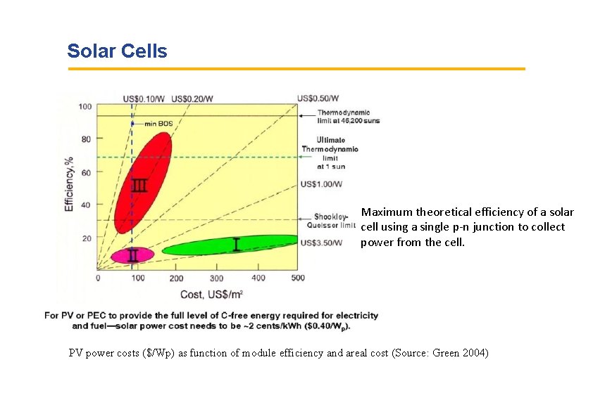
Solar Cells Maximum theoretical efficiency of a solar cell using a single p-n junction to collect power from the cell. PV power costs ($/Wp) as function of module efficiency and areal cost (Source: Green 2004)

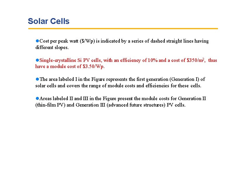
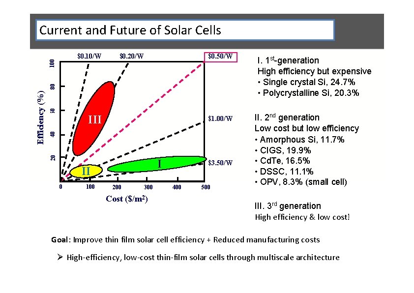
Solar Cells Cost per peak watt ($/Wp) is indicated by a series of dashed straight lines having different slopes. Single-crystalline Si PV cells, with an efficiency of 10% and a cost of $350/m 2, thus have a module cost of $3. 50/Wp. The area labeled I in the Figure represents the first generation (Generation I) of solar cells and covers the range of module costs and efficiencies for these cells. Areas labeled II and III in the Figure present the module costs for Generation II (thin-film PV) and Generation III (advanced future structures) PV cells.

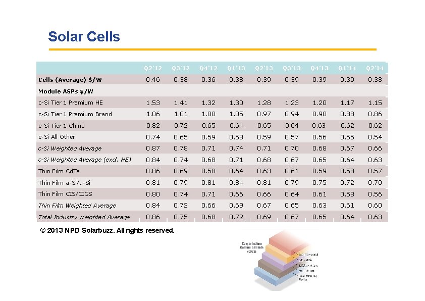
Solar Cells Q 2’ 12 Q 3’ 12 Q 4’ 12 Q 1’ 13 Q 2’ 13 Q 3’ 13 Q 4’ 13 Q 1’ 14 Q 2’ 14 0. 46 0. 38 0. 39 0. 38 c-Si Tier 1 Premium HE 1. 53 1. 41 1. 32 1. 30 1. 28 1. 23 1. 20 1. 17 1. 15 c-Si Tier 1 Premium Brand 1. 06 1. 01 1. 00 1. 05 0. 97 0. 94 0. 90 0. 88 0. 86 c-Si Tier 1 China 0. 82 0. 72 0. 65 0. 64 0. 63 0. 62 c-Si All Other 0. 74 0. 65 0. 59 0. 58 0. 59 0. 57 0. 56 0. 55 0. 54 c-Si Weighted Average 0. 87 0. 78 0. 71 0. 74 0. 71 0. 70 0. 68 0. 67 0. 66 c-Si Weighted Average (excl. HE) 0. 84 0. 74 0. 68 0. 71 0. 68 0. 67 0. 65 0. 64 0. 63 Thin Film Cd. Te 0. 86 0. 69 0. 58 0. 64 0. 63 0. 61 0. 59 0. 58 0. 57 Thin Film a-Si/μ-Si 0. 81 0. 79 0. 81 0. 84 0. 81 0. 79 0. 75 0. 72 0. 70 Thin Film CIS/CIGS 0. 80 0. 74 0. 71 0. 66 0. 64 0. 61 0. 58 0. 56 Thin Film Weighted Average 0. 84 0. 72 0. 66 0. 69 0. 67 0. 65 0. 63 0. 61 0. 60 Total Industry Weighted Average 0. 86 0. 75 0. 68 0. 72 0. 69 0. 67 0. 65 0. 64 0. 63 Cells (Average) $/W Module ASPs $/W © 2013 NPD Solarbuzz. All rights reserved.

Solar Cells © 2013 NPD Solarbuzz. All rights reserved.

Current and Future of Solar Cells $0. 20/W $0. 50/W 60 III 40 $1. 00/W 20 Efficiency (%) 80 100 $0. 10/W I II 0 100 200 300 Cost ($/m 2) $3. 50/W 400 500 I. 1 st-generation High efficiency but expensive • Single crystal Si, 24. 7% • Polycrystalline Si, 20. 3% II. 2 nd generation Low cost but low efficiency • Amorphous Si, 11. 7% • CIGS, 19. 9% • Cd. Te, 16. 5% • DSSC, 11. 1% • OPV, 8. 3% (small cell) III. 3 rd generation High efficiency & low cost! Goal: Improve thin film solar cell efficiency + Reduced manufacturing costs Ø High-efficiency, low-cost thin-film solar cells through multiscale architecture

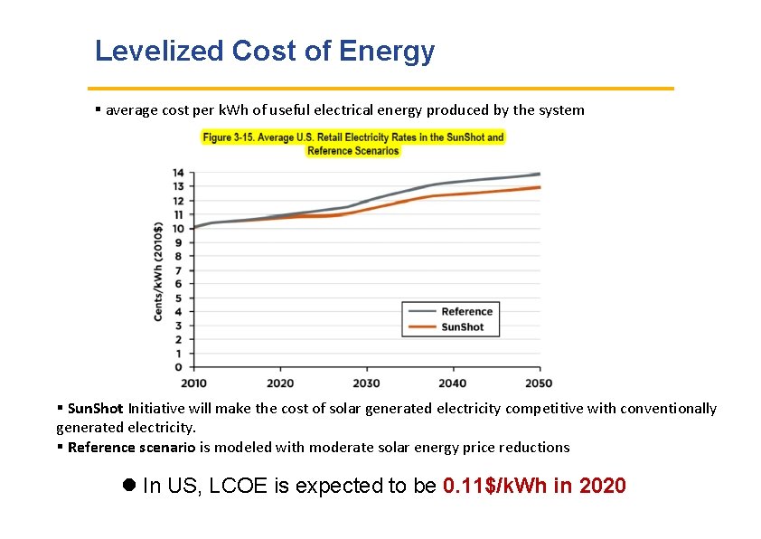
Levelized Cost of Energy average cost per k. Wh of useful electrical energy produced by the system Sun. Shot Initiative will make the cost of solar generated electricity competitive with conventionally generated electricity. Reference scenario is modeled with moderate solar energy price reductions In US, LCOE is expected to be 0. 11$/k. Wh in 2020

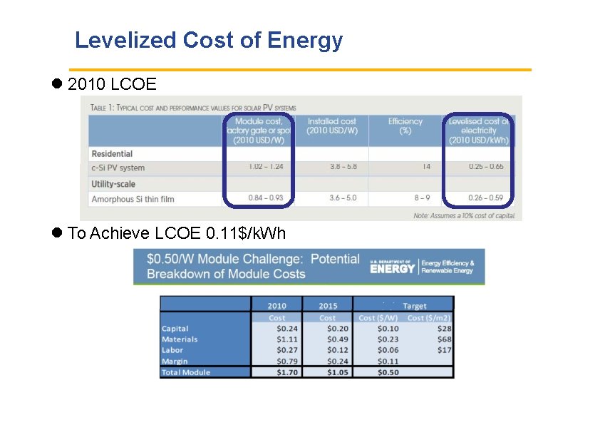
Levelized Cost of Energy 2010 LCOE To Achieve LCOE 0. 11$/k. Wh

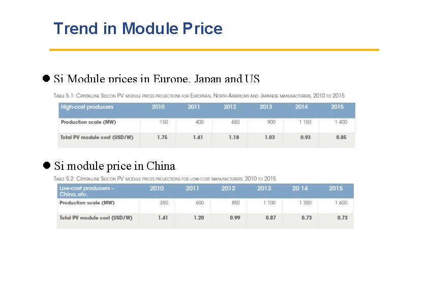
Trend in Module Price Si Module prices in Europe, Japan and US Si module price in China

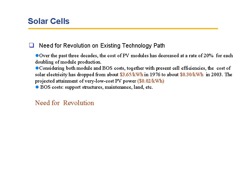
Solar Cells Need for Revolution on Existing Technology Path Over the past three decades, the cost of PV modules has decreased at a rate of 20% for each doubling of module production. Considering both module and BOS costs, together with present cell efficiencies, the cost of solar electricity has dropped from about $3. 65/k. Wh in 1976 to about $0. 30/k. Wh in 2003. The projected attainment of very-low-cost PV power ($0. 02/k. Wh) BOS costs: support structures, maintenance, land, etc. Need for Revolution

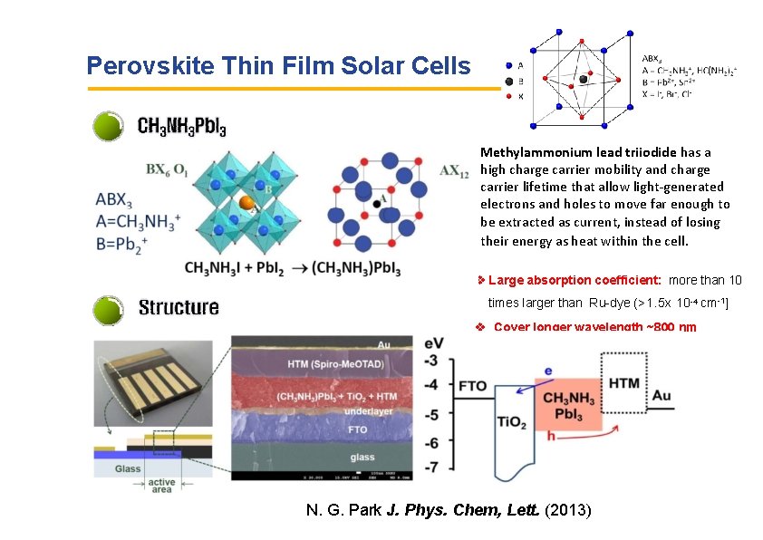
Perovskite Thin Film Solar Cells Methylammonium lead triiodide has a high charge carrier mobility and charge carrier lifetime that allow light-generated electrons and holes to move far enough to be extracted as current, instead of losing their energy as heat within the cell. Large absorption coefficient: more than 10 times larger than Ru-dye (>1. 5 x 10 -4 cm-1] Cover longer wavelength ~800 nm N. G. Park J. Phys. Chem, Lett. (2013)

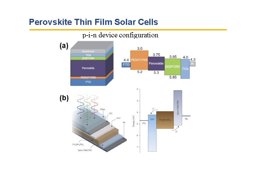
Perovskite Thin Film Solar Cells p-i-n device configuration n-i-p device configuration

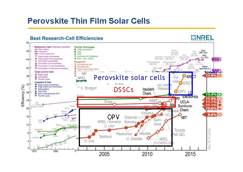
Perovskite Thin Film Solar Cells Perovskite solar cells DSSCs OPV

Perovskite Thin Film Solar Cells

Solar Cells Conduction in Semiconductors The electrons in the covalent bond formed between each of the atoms in the lattice structure are held in place by this bond and hence they are localized to the region surrounding the atom. These bonded electrons cannot move or change energy, and thus are not considered "free" and cannot participate in current flow. However, only at absolute zero are all electrons in this "stuck, " bonded arrangement. At elevated temperatures, especially at the temperatures where solar cells operate, electrons can gain enough energy to escape from their bonds. When this happens, the electrons are free to move about the crystal lattice and participate in conduction. At room temperature, a semiconductor has enough free electrons to allow it to conduct current. When an electron gains enough energy to participate in conduction (is "free"), it is at a high energy state. When the electron is bound, and thus cannot participate in conduction, the electron is at a low energy state. it is either at a low energy position in the bond, or it has gained enough energy to break free and therefore has a certain minimum energy. This minimum energy is called the "band gap" of a semiconductor.

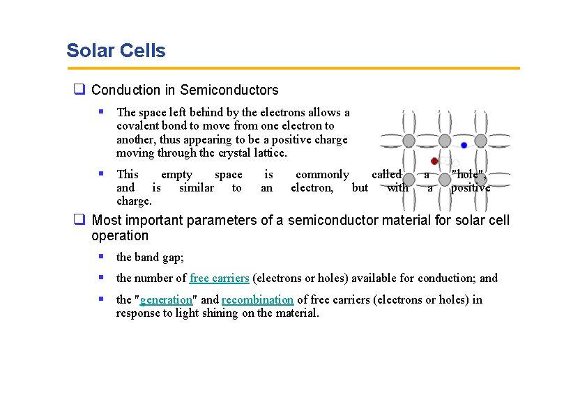
Solar Cells Conduction in Semiconductors The space left behind by the electrons allows a covalent bond to move from one electron to another, thus appearing to be a positive charge moving through the crystal lattice. This and charge. empty space is similar to is an commonly called electron, but with a a "hole", positive Most important parameters of a semiconductor material for solar cell operation the band gap; the number of free carriers (electrons or holes) available for conduction; and the "generation" and recombination of free carriers (electrons or holes) in response to light shining on the material.

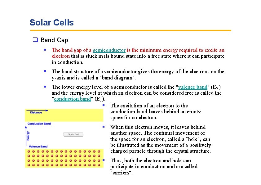
Solar Cells Band Gap The band gap of a semiconductor is the minimum energy required to excite an electron that is stuck in its bound state into a free state where it can participate in conduction. The band structure of a semiconductor gives the energy of the electrons on the y-axis and is called a "band diagram". The lower energy level of a semiconductor is called the "valence band" (EV) and the energy level at which an electron can be considered free is called the "conduction band" (EC). The excitation of an electron to the conduction band leaves behind an empty space for an electron. When this electron moves, it leaves behind another space. The continual movement of the space for an electron, called a "hole", can be illustrated as the movement of a positively charged particle through the crystal structure. Thus, both the electron and hole can participate in conduction and are called "carriers".

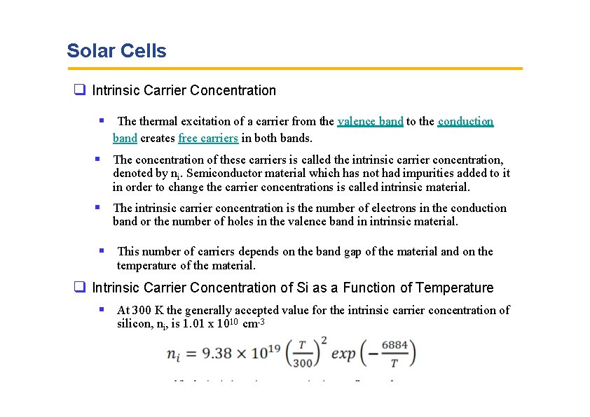
Solar Cells Intrinsic Carrier Concentration The thermal excitation of a carrier from the valence band to the conduction band creates free carriers in both bands. The concentration of these carriers is called the intrinsic carrier concentration, denoted by ni. Semiconductor material which has not had impurities added to it in order to change the carrier concentrations is called intrinsic material. The intrinsic carrier concentration is the number of electrons in the conduction band or the number of holes in the valence band in intrinsic material. This number of carriers depends on the band gap of the material and on the temperature of the material. Intrinsic Carrier Concentration of Si as a Function of Temperature At 300 K the generally accepted value for the intrinsic carrier concentration of silicon, ni, is 1. 01 x 1010 cm-3