Project Review Of Parallel Chip Set for WaveletBased
Project Review Of Parallel Chip Set for Wavelet-Based Motion Estimation for MPEG-4 Video Compression University of Pittsburgh Department of Electrical Engineering (In Collaboration with OKI Semiconductor) Co-Principal Investigators: C. C. Li, Henry Y. H. Chuang, and Steven P. Levitan Research Assistants: Li-Chang Liu, James J. C. Chien, and David P. Birch Undergraduate Trainee: Fellen F-W Yang April 24, 2002
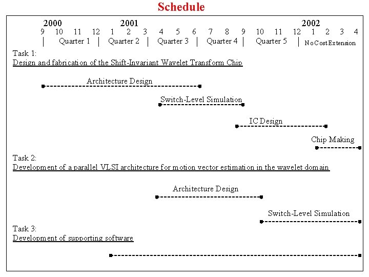
Schedule 2000 9 10 11 12 Quarter 1 2001 1 2 3 Quarter 2 4 5 6 Quarter 3 7 8 9 Quarter 4 2002 10 11 12 1 2 3 4 Quarter 5 No Cost Extension Task 1: Design and fabrication of the Shift-Invariant Wavelet Transform Chip Architecture Design Switch-Level Simulation IC Design Chip Making Task 2: Development of a parallel VLSI architecture for motion vector estimation in the wavelet domain Architecture Design Switch-Level Simulation Task 3: Development of supporting software
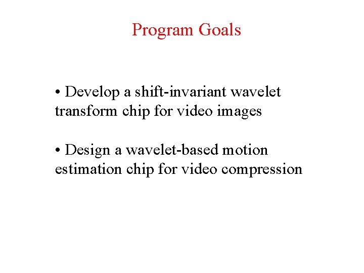
Program Goals • Develop a shift-invariant wavelet transform chip for video images • Design a wavelet-based motion estimation chip for video compression
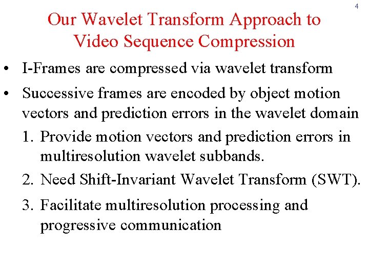
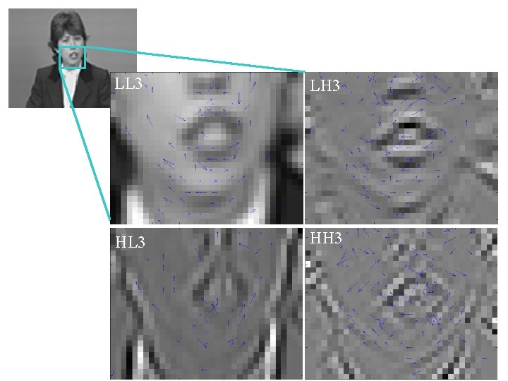
Our Wavelet Transform Approach to Video Sequence Compression 4 • I-Frames are compressed via wavelet transform • Successive frames are encoded by object motion vectors and prediction errors in the wavelet domain 1. Provide motion vectors and prediction errors in multiresolution wavelet subbands. 2. Need Shift-Invariant Wavelet Transform (SWT). 3. Facilitate multiresolution processing and progressive communication
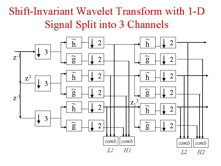
Shift-Invariant Wavelet Transform with 1 -D Signal Split into 3 Channels 3 z-1 z 3 3 z-1 2 2 2 2 z 13 2 2 2 comb L 1 H 1 comb L 2 H 2
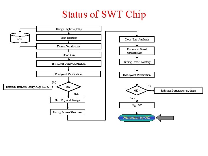
Status of SWT Chip Design Capture (RTL) Scan Insertion RTL Formal Verification Floor-Plan Pre-layout Delay Calculation Pre-layout Verification Clock Tree Synthesis Placement Based Optimization Timing Driven Routing Post-layout Verification NO Reiterate from necessary stage (RTL) No OK? YES Start Physical Design OK? Yes Sign Off Timing Driven Placement Fabrication by OKI Reiterate from necessary stage
7 Progress of ME Chip Design (Frame-level Pipelined Full-Search Motion Estimation) • A minor change of the middle PE in the processor facilitates to generate zero vectors in the motionless background. • Minimize Sel 1 and Sel 2 control signal inputs by propagating them through the array. • Complete Model. Sim verification of the processor array.
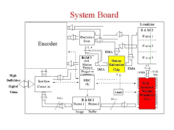
System Board Encoder
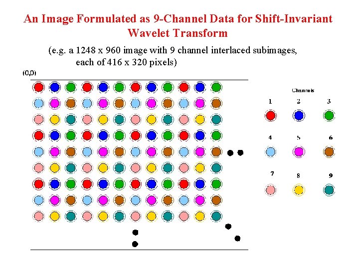
An Image Formulated as 9 -Channel Data for Shift-Invariant Wavelet Transform (e. g. a 1248 x 960 image with 9 channel interlaced subimages, each of 416 x 320 pixels)
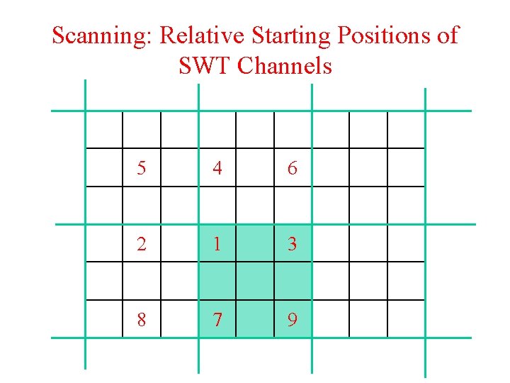
Scanning: Relative Starting Positions of SWT Channels 5 4 6 2 1 3 8 7 9
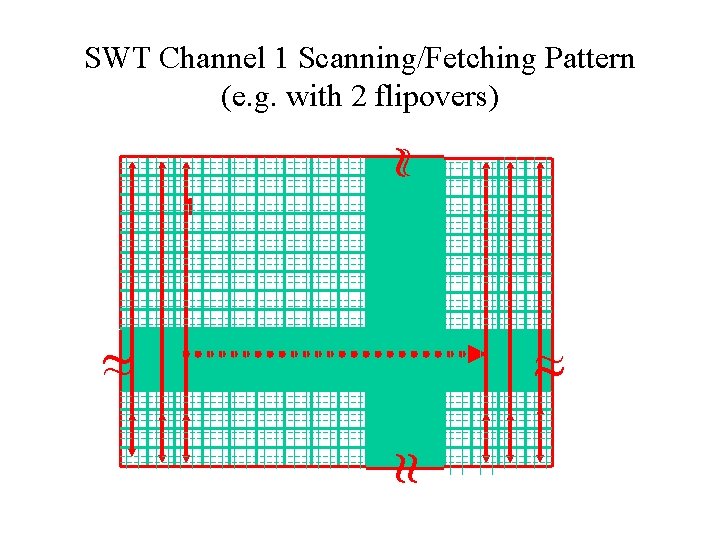
SWT Channel 1 Scanning/Fetching Pattern (e. g. with 2 flipovers) ~ ~ ~ ~
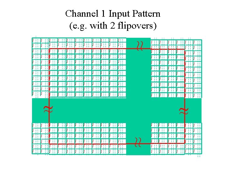
Channel 1 Input Pattern (e. g. with 2 flipovers) 1 1 1 1 1 1 1 1 1 1 1 1 1 1 1 1 1 1 1 1 1 1 1 1 1 1 1 1 ~ ~ 1 1 1 1 1 1 1 1 1 1 1 1 1 1 1 1 1 ~ ~ 1 1 1 1 1 1 1 1 1 1 1 1 1 1 1 1 1 1 1 1 1 1 1 1 1 1 1 1 1
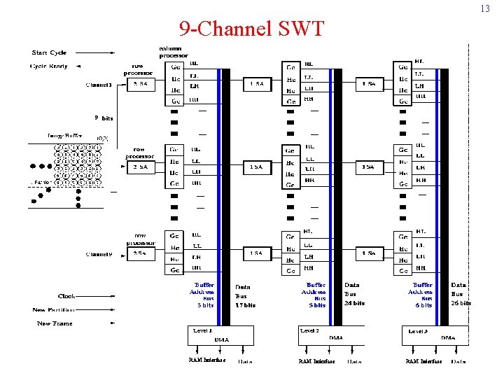
13 9 -Channel SWT 9 7 RAM Interface
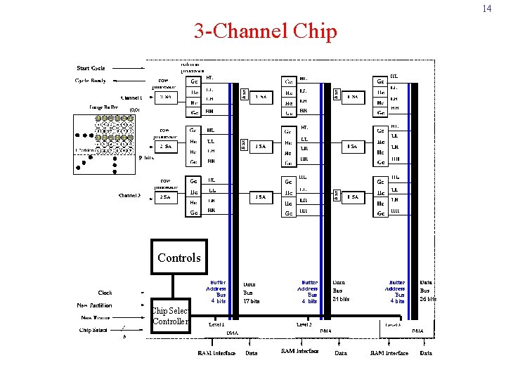
14 3 -Channel Chip reg reg 9 reg Controls 4 Chip Select Controller 4 4
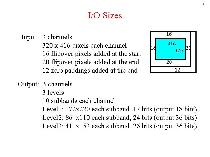
15 I/O Sizes Input: 3 channels 320 x 416 pixels each channel 16 flipover pixels added at the start 20 flipover pixels added at the end 12 zero paddings added at the end 16 16 416 20 320 20 12 Output: 3 channels 3 levels 10 subbands each channel Level 1: 172 x 220 each subband, 17 bits (output 18 bits) Level 2: 86 x 110 each subband, 24 bits (output 36 bits) Level 3: 41 x 53 each subband, 26 bits (output 36 bits)
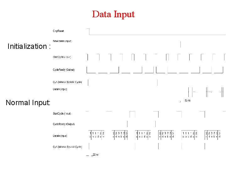
Data Input Initialization : Normal Input:
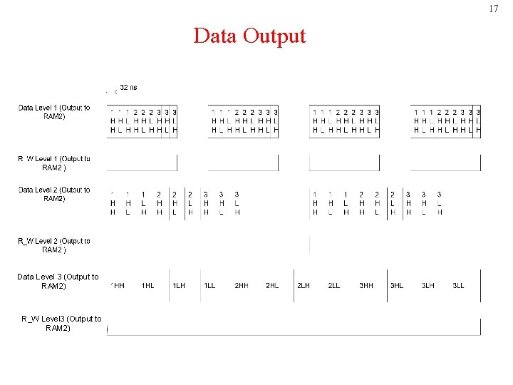
17 Data Output Data Level 3 (Output to RAM 2) R_W Level 3 (Output to RAM 2)
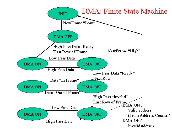
INIT DMA: Finite State Machine New. Frame “Low” DMA OFF DMA ON High Pass Data “Ready” New. Frame “High” First Row of Frame Low Pass Data DMA OFF High Pass Data Low Pass Data “Ready” Next Row Data “In Frame” DMA ON DMA OFF Data “Out of Frame” Low Pass Data DMA ON High Pass Data High Pass “Invalid” Last Row of Frame DMA ON : Valid address DMA OFF (From Address Counter) DMA OFF: Invalid address
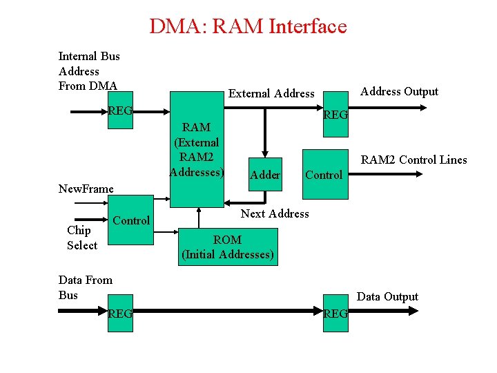
DMA: RAM Interface Internal Bus Address From DMA Address Output External Address REG RAM (External RAM 2 Addresses) REG RAM 2 Control Lines Adder Control New. Frame Chip Select Control Data From Bus REG Next Address ROM (Initial Addresses) Data Output REG
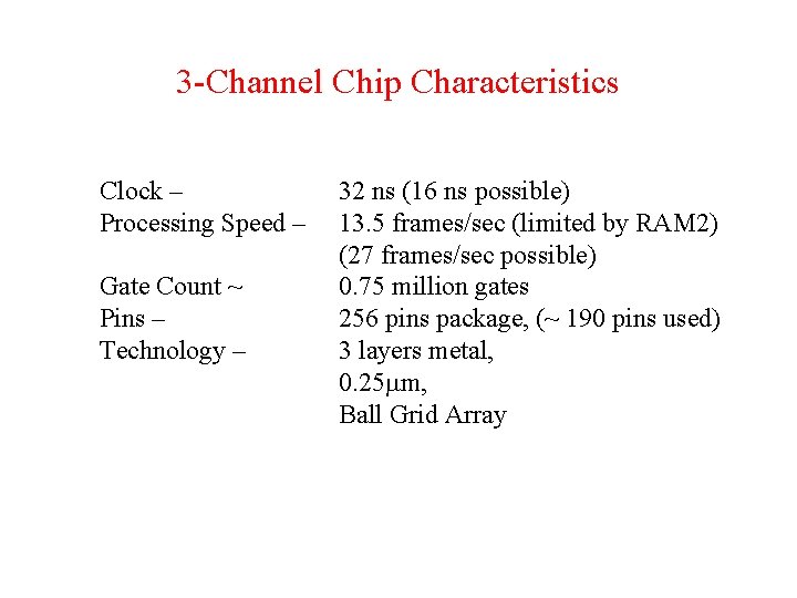
3 -Channel Chip Characteristics Clock – Processing Speed – Gate Count ~ Pins – Technology – 32 ns (16 ns possible) 13. 5 frames/sec (limited by RAM 2) (27 frames/sec possible) 0. 75 million gates 256 pins package, (~ 190 pins used) 3 layers metal, 0. 25 mm, Ball Grid Array
LL 3 LH 3 HL 3 HH 3
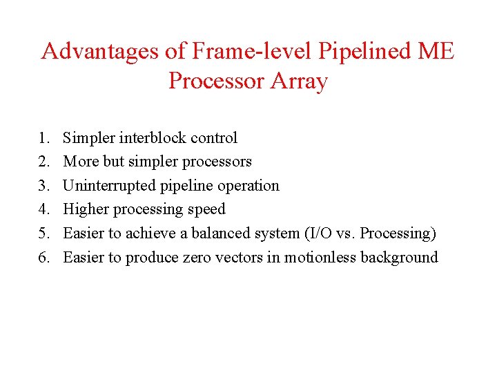
Advantages of Frame-level Pipelined ME Processor Array 1. 2. 3. 4. 5. 6. Simpler interblock control More but simpler processors Uninterrupted pipeline operation Higher processing speed Easier to achieve a balanced system (I/O vs. Processing) Easier to produce zero vectors in motionless background
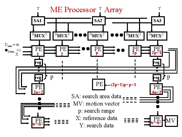
Y ME Processor SA 1 Dmin = ¥ l. Dmin =1 X Y Array Y SA 2 0 MUX 1 PE PE PE 1 2 SA 3 0 MUX 1 PE p 2 p reg PE 2 p+2 PE 4 p +2 p+1 2 0 MUX 1 PE 2 p+1 reg p reg PE (2 p+1)p+p+1 SA: search area data MV: motion vector p: search range X: reference data Y: search data p PE 4 p+2 PE MV 4 p 2+4 p+1
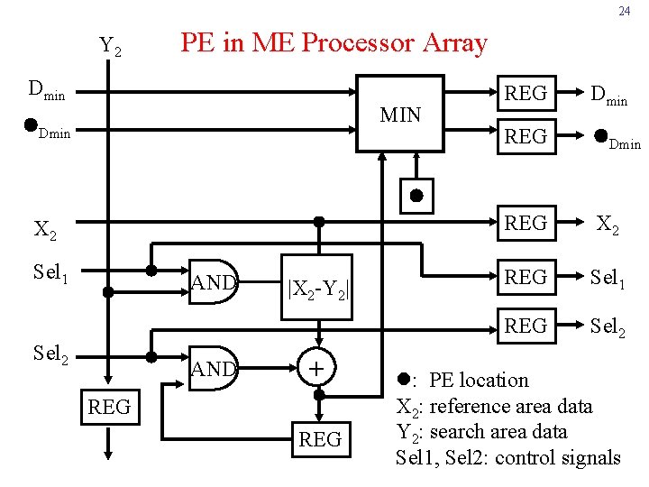
24 Y 2 PE in ME Processor Array Dmin MIN l. Dmin REG X 2 REG Sel 1 REG Sel 2 l X 2 Sel 1 AND Sel 2 AND |X 2 -Y 2| + REG l: PE location X 2: reference area data Y 2: search area data Sel 1, Sel 2: control signals
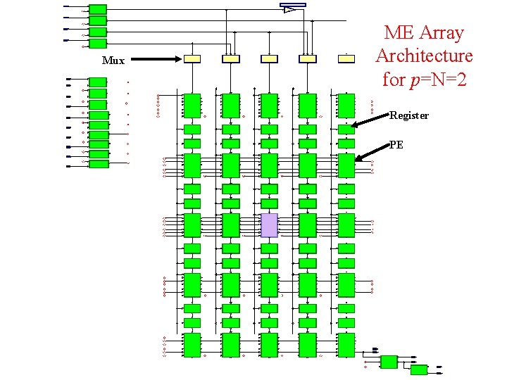
Mux ME Array Architecture for p=N=2 Register PE
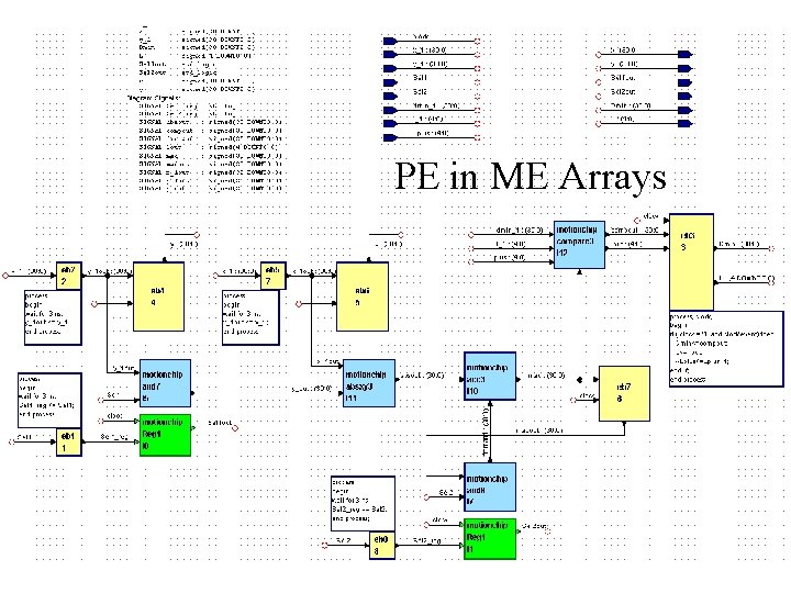
PE in ME Arrays
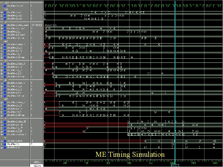
ME Timing Simulation
Deliverables • Synthesizable VHDL code of shift-invariant wavelet transform chip, chip design, test chips, test data, and documentation, synthesized netlist, layout netlist. • VHDL code of wavelet-based motion estimation for video compression, test data, and documentation • Technical Report • Supporting Softwares Simulator of SWT and ME Architectures in Matlab SWT and ME Test Data Generators in Matlab SWT Input Fetching Pseudocode SWT Output Test Data Generator

End of Presentation …
- Slides: 29