Progress of SOI Pixel sensor RD T Tsuboyama
Progress of SOI Pixel sensor R&D T. Tsuboyama (KEK) 1 Ottobre 2014

Monolithic Pixel detector • Necessary for large scale, low-material-budget vertex detectors in the high-energy physics experiments. – Separating vertices in HL-LHC. – Identifying b and c particles with high efficiency (ILC/LHC) – Reduction of hit occupancy. • Comparison with hybrid pixel detectors – No bumps higher production yield, cost – Thinning is easier. – Cooling is an important issue common to all types of detector. • On going R&Ds: DEPFET, MAPS, SOI, CCD… – All technologies have pros and cons. – SOI came later, however, we try to catch up the R&D. 1 Ottobre 2014 2

Lapis (Oki) SOI technology • The 0. 2 μm CMOS circuit is build above the "sensor grade" Si wafers, separated with 200 nm thick Si. O 2 layer, called as BOX. – OKI Semiconductor company was absorbed by Rohm and changed the name as Lapis Semiconductor. • The signal induced in the wafer is read out with the CMOS circuit on the top. • Whole semiconductor process is done in Lapis SOI CMOS commercial process. • The thickness of the sensor part can be changed from 50 to 700 um depending on the application. 1 Ottobre 2014 CMOS (Low Resistivity) Si. O 2 (BOX) Sensor (High Resistivity) 3

A Grant-in-Aid Project • Please visit "http: //www. soipix. jp/index_en. html". • The project contains not only particle physics groups but also groups of astronomy, material science, nondestructive inspection, biology, medical… 1 Ottobre 2014 4
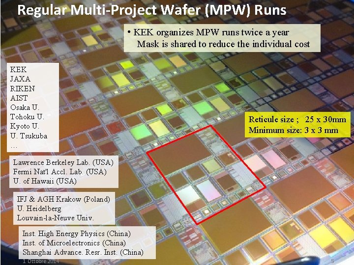
Regular Multi-Project Wafer (MPW) Runs • KEK organizes MPW runs twice a year Mask is shared to reduce the individual cost KEK JAXA RIKEN AIST Osaka U. Tohoku U. Kyoto U. U. Tsukuba … Reticule size ; 25 x 30 mm Minimum size: 3 x 3 mm Lawrence Berkeley Lab. (USA) Fermi Nat'l Accl. Lab. (USA) U. of Hawaii (USA) IFJ & AGH Krakow (Poland) U. Heidelberg Louvain-la-Neuve Univ. Inst. High Energy Physics (China) Inst. of Microelectronics (China) Shanghai Advance. Resr. Inst. (China) 1 Ottobre 2014 5
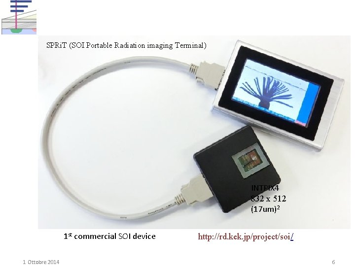
6 SPRi. T (SOI Portable Radiation imaging Terminal) INTPIX 4 832 x 512 (17 um)2 1 st commercial SOI device 1 Ottobre 2014 http: //rd. kek. jp/project/soi/ 6
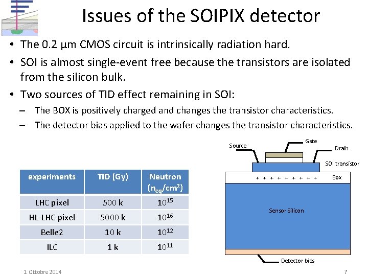
Issues of the SOIPIX detector • The 0. 2 μm CMOS circuit is intrinsically radiation hard. • SOI is almost single-event free because the transistors are isolated from the silicon bulk. • Two sources of TID effect remaining in SOI: – The BOX is positively charged and changes the transistor characteristics. – The detector bias applied to the wafer changes the transistor characteristics. Gate Source Drain SOI transistor experiments TID (Gy) Neutron (neq/cm 2) LHC pixel 500 k 1015 HL-LHC pixel 5000 k 1016 Belle 2 10 k 1012 ILC 1 k 1011 + + + + + Box Sensor Silicon Detector bias 1 Ottobre 2014 7
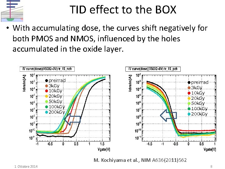
TID effect to the BOX • With accumulating dose, the curves shift negatively for both PMOS and NMOS, influenced by the holes accumulated in the oxide layer. ●preirrad ● 3 k. Gy ● 10 k. Gy ● 20 k. Gy ● 50 k. Gy ● 100 k. Gy ● 200 k. Gy M. Kochiyama et al. , NIM A 636(2011)S 62 1 Ottobre 2014 8
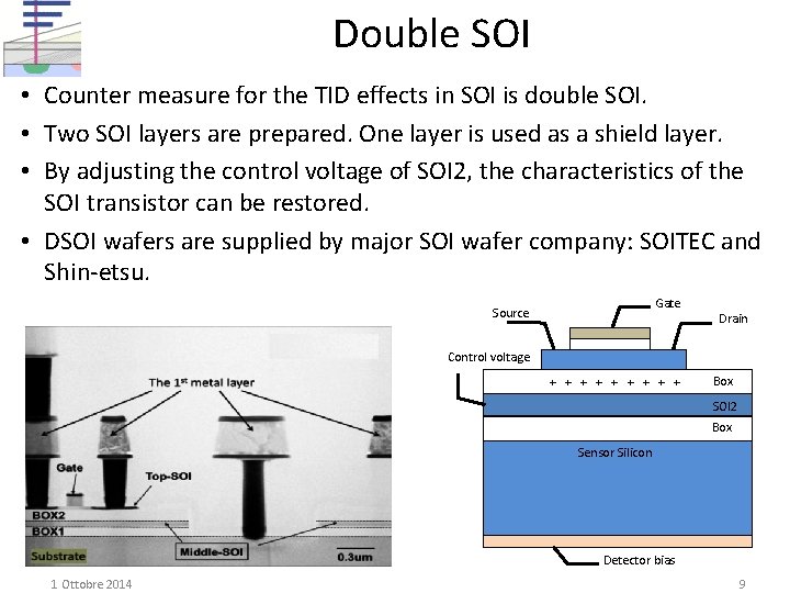
Double SOI • Counter measure for the TID effects in SOI is double SOI. • Two SOI layers are prepared. One layer is used as a shield layer. • By adjusting the control voltage of SOI 2, the characteristics of the SOI transistor can be restored. • DSOI wafers are supplied by major SOI wafer company: SOITEC and Shin-etsu. Gate Source Drain Control voltage + + + + + Box SOI 2 Box Sensor Silicon Detector bias 1 Ottobre 2014 9
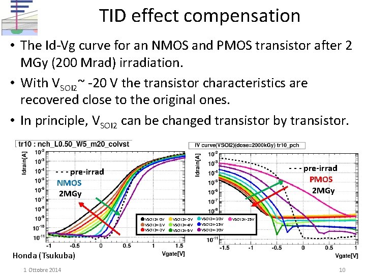
TID effect compensation Threshold voltage • The Id-Vg curve for an NMOS and PMOS transistor after 2 MGy (200 Mrad) irradiation. • With VSOI 2~ -20 V the transistor characteristics are recovered close to the original ones. • In principle, VSOI 2 can be changed transistor by transistor. NMOS - - - pre-irrad NMOS 2 MGy PMOS preirrad - - - pre-irrad PMOS 2 MGy ●VSOI 2= 0 V ●VSOI 2=-3 V ●VSOI 2=-10 V ●VSOI 2=-25 V ●VSOI 2=-1 V ●VSOI 2=-4 V ●VSOI 2=-15 V ●VSOI 2=-2 V ●VSOI 2=-5 V ●VSOI 2=-20 V preirrad Honda (Tsukuba) 1 Ottobre 2014 10
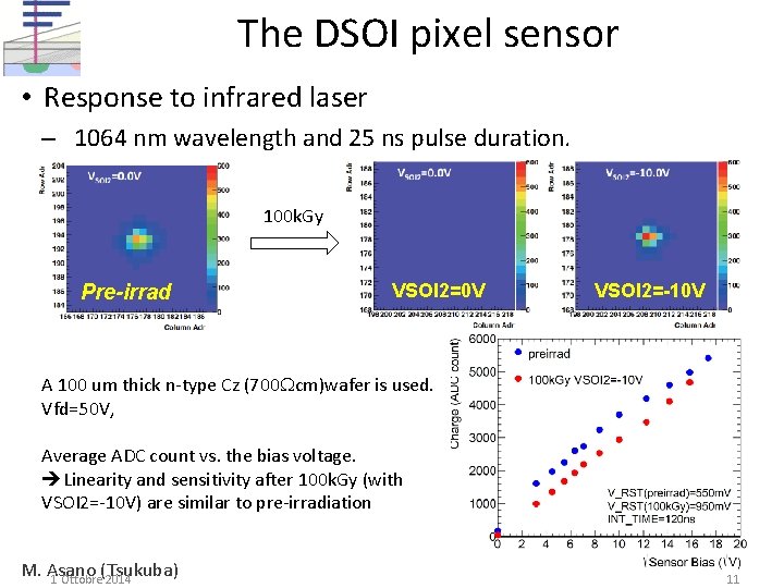
The DSOI pixel sensor • Response to infrared laser – 1064 nm wavelength and 25 ns pulse duration. 100 k. Gy Pre-irrad VSOI 2=0 V VSOI 2=-10 V A 100 um thick n-type Cz (700 Wcm)wafer is used. Vfd=50 V, Average ADC count vs. the bias voltage. Linearity and sensitivity after 100 k. Gy (with VSOI 2=-10 V) are similar to pre-irradiation M. Asano (Tsukuba) 1 Ottobre 2014 11
PIXOR: Application to Belle 2 • In order to proceed a realistic design, a Belle 2 model is prepared: PIXOR • PIXOR type pixel sensor: • Tohoku University is the development center. – The Pioneering work was made Y. Onuki and S. Ono in 2011. – The R&D is continued by A. Ishikawa, N. Shinoda, and I. Ushiki in 2014. 1 Ottobre 2014 12
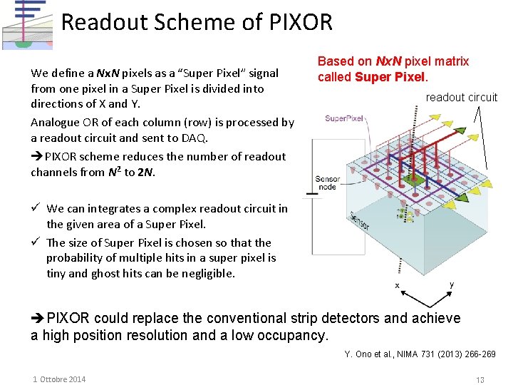
Readout Scheme of PIXOR We define a Nx. N pixels as a “Super Pixel” signal from one pixel in a Super Pixel is divided into directions of X and Y. Analogue OR of each column (row) is processed by a readout circuit and sent to DAQ. PIXOR scheme reduces the number of readout channels from N 2 to 2 N. Based on Nx. N pixel matrix called Super Pixel. readout circuit ü We can integrates a complex readout circuit in the given area of a Super Pixel. ü The size of Super Pixel is chosen so that the probability of multiple hits in a super pixel is tiny and ghost hits can be negligible. PIXOR could replace the conventional strip detectors and achieve a high position resolution and a low occupancy. Y. Ono et al. , NIMA 731 (2013) 266 -269 1 Ottobre 2014 13
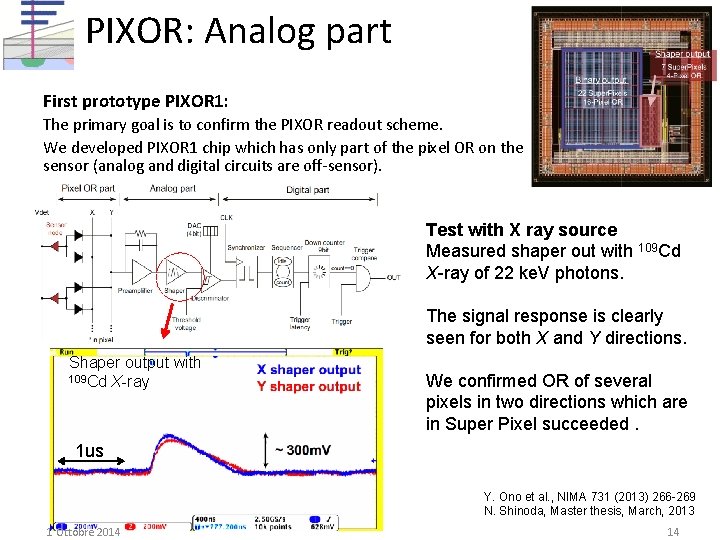
PIXOR: Analog part First prototype PIXOR 1: The primary goal is to confirm the PIXOR readout scheme. We developed PIXOR 1 chip which has only part of the pixel OR on the sensor (analog and digital circuits are off-sensor). Test with X ray source Measured shaper out with 109 Cd X-ray of 22 ke. V photons. The signal response is clearly seen for both X and Y directions. Shaper output with 109 Cd X-ray We confirmed OR of several pixels in two directions which are in Super Pixel succeeded. 1 us Y. Ono et al. , NIMA 731 (2013) 266 -269 N. Shinoda, Master thesis, March, 2013 1 Ottobre 2014 14
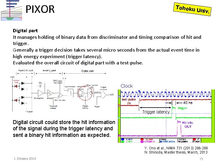
PIXOR Tohoku Univ. Digital part It manages holding of binary data from discriminator and timing comparison of hit and trigger. Generally a trigger decision takes several micro seconds from the actual event time in high energy experiment (trigger latency). Evaluated the overall circuit of digital part with a test-pulse. Clock Trigger latency Digital circuit could store the hit information of the signal during the trigger latency and sent a binary hit information as expected. Y. Ono et al. , NIMA 731 (2013) 266 -269 N. Shinoda, Master thesis, March, 2013 1 Ottobre 2014 15
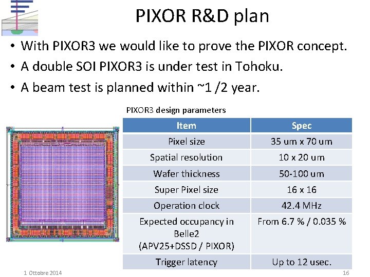
PIXOR R&D plan • With PIXOR 3 we would like to prove the PIXOR concept. • A double SOI PIXOR 3 is under test in Tohoku. • A beam test is planned within ~1 /2 year. PIXOR 3 design parameters 1 Ottobre 2014 Item Spec Pixel size 35 um x 70 um Spatial resolution 10 x 20 um Wafer thickness 50 -100 um Super Pixel size 16 x 16 Operation clock 42. 4 MHz Expected occupancy in Belle 2 (APV 25+DSSD / PIXOR) From 6. 7 % / 0. 035 % Trigger latency Up to 12 usec. 16
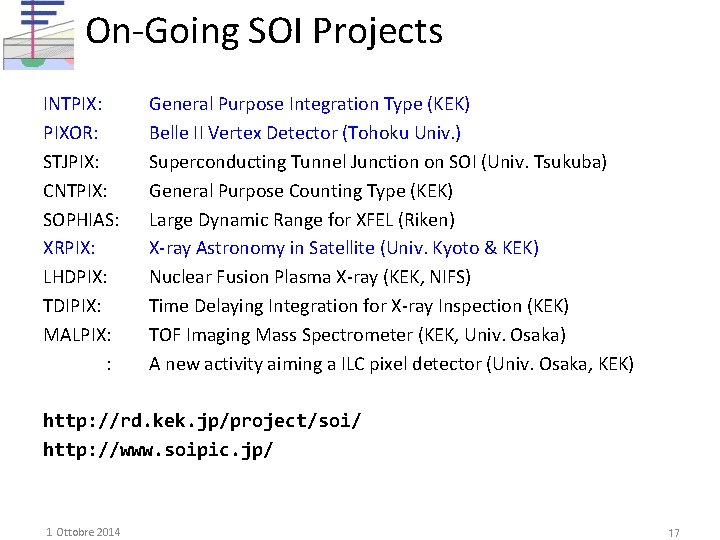
On-Going SOI Projects INTPIX: PIXOR: STJPIX: CNTPIX: SOPHIAS: XRPIX: LHDPIX: TDIPIX: MALPIX: : General Purpose Integration Type (KEK) Belle II Vertex Detector (Tohoku Univ. ) Superconducting Tunnel Junction on SOI (Univ. Tsukuba) General Purpose Counting Type (KEK) Large Dynamic Range for XFEL (Riken) X-ray Astronomy in Satellite (Univ. Kyoto & KEK) Nuclear Fusion Plasma X-ray (KEK, NIFS) Time Delaying Integration for X-ray Inspection (KEK) TOF Imaging Mass Spectrometer (KEK, Univ. Osaka) A new activity aiming a ILC pixel detector (Univ. Osaka, KEK) http: //rd. kek. jp/project/soi/ http: //www. soipic. jp/ 1 Ottobre 2014 17
Summary • SOI is a potential technology for the pixel vertex detectors. • The TID effects can be mitigated with the double SOI technology. • Recently a DSOI pixel detector worked up to 100 k. Gy irradiation. • PIXOR type detector R&D is in progress. After PIXOR 3 is proved with a beam test, a full size detector will be made. This is a preparation of Belle 2 SVD upgrade. 1 Ottobre 2014 18
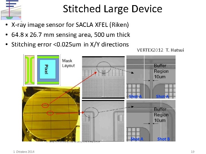
Stitched Large Device 1919 • X-ray image sensor for SACLA XFEL (Riken) • 64. 8 x 26. 7 mm sensing area, 500 um thick • Stitching error <0. 025 um in X/Y directions VERTEX 2012 T. Hatsui K. Hara, VERTEX 2014, Macha Lake, Czech Sep. 16 -19 1 Ottobre 2014 19
- Slides: 19