
Progress and Challenges toward 100 Gbps Ethernet Joel
Progress and Challenges toward 100 Gbps Ethernet Joel Goergen VP of Technology / Chief Scientist 1 Abstract: This technical presentation will focus on the progress and challenges for development of technology and standards for 100 Gb. E. Joel is an active contributor to IEEE 802. 3 and the Optical Internetworking Forum (OIF) standards process. Joel will discuss design methodology, enabling technologies, emerging specifications, and crucial considerations for performance and reliability for this next iteration of LAN/WAN technology.
Overview 2 n Network Standards Today n Available Technology Today n Feasible Technology for 2009 n The Push for Standards within IEEE and OIF n Anatomy of a 100 Gbps or 160 Gbps Solution n Summary n Backup Slides
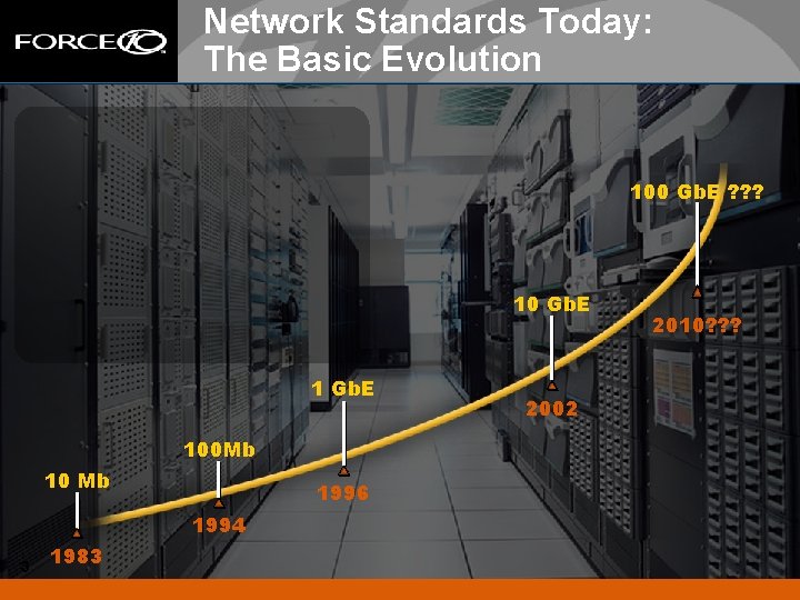
Network Standards Today: The Basic Evolution 100 Gb. E ? ? ? 10 Gb. E 100 Mb 10 Mb 1996 1994 3 1983 2002 2010? ? ?

Network Standards Today: The Basic Structure 4
Network Standards Today: The Desk top n 1 Gbps Ethernet – 10/1000 Copper ports have been shipping with most desktop and laptop machines for a few years. – Fiber SMF/MMF n IEEE 802. 11 a/b/g Wireless – Average useable bandwidth reaching 50 Mbps 5
Network Standards Today: Clusters and Servers n 1 Gbps Ethernet – Copper n 10 Gbps Ethernet – Fiber – CX-4 6
Network Standards Today: Coming Soon n 10 Gbps LRM – Multi-mode fiber to 220 meters. n 10 Gbps Base-T – 100 meters at more then 10 Watts per port ? ? ? – 30 meters short reach at 3 Watts per port ? ? ? n 10 Gbps Back Plane – 1 Gbps, 4 x 3. 125 Gbps, 1 x 10 Gbps over 1 meter improved fr-4 material. 7
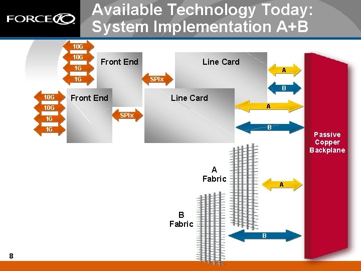
Available Technology Today: System Implementation A+B 10 G 1 G Front End Line Card A 1 G SPIx B 10 G Line Card Front End A 10 G 1 G SPIx B 1 G A Fabric A B Fabric B 8 Passive Copper Backplane
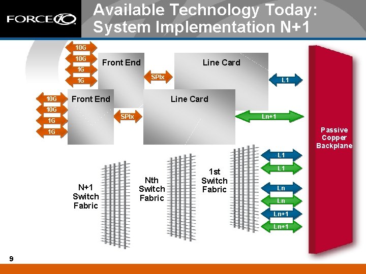
Available Technology Today: System Implementation N+1 10 G 1 G Front End SPIx 1 G 10 G Line Card Front End 10 G L 1 SPIx 1 G Ln+1 Passive Copper Backplane 1 G L 1 N+1 Switch Fabric Nth Switch Fabric 1 st Switch Fabric L 1 Ln Ln Ln+1 9
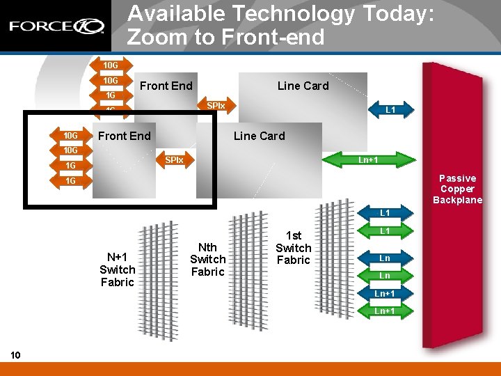
Available Technology Today: Zoom to Front-end 10 G 1 G Front End SPIx 1 G 10 G Line Card Front End 10 G L 1 SPIx 1 G Ln+1 Passive Copper Backplane 1 G L 1 N+1 Switch Fabric Nth Switch Fabric 1 st Switch Fabric L 1 Ln Ln Ln+1 10
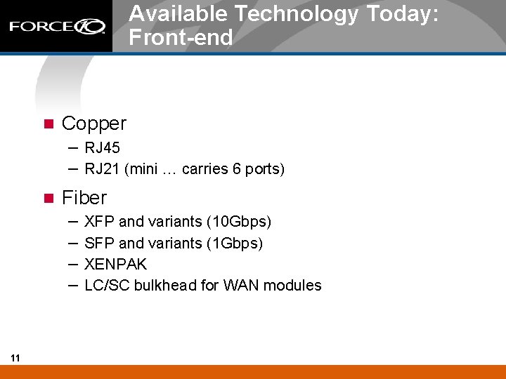
Available Technology Today: Front-end n Copper – RJ 45 – RJ 21 (mini … carries 6 ports) n Fiber – – 11 XFP and variants (10 Gbps) SFP and variants (1 Gbps) XENPAK LC/SC bulkhead for WAN modules
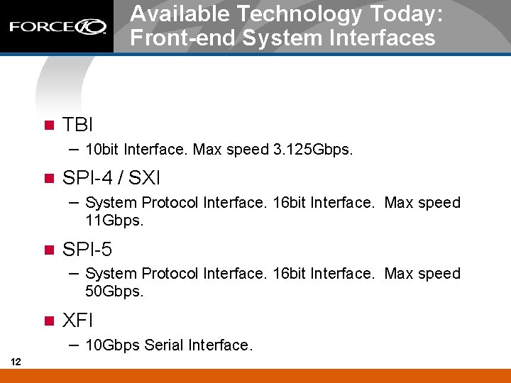
Available Technology Today: Front-end System Interfaces n TBI – 10 bit Interface. Max speed 3. 125 Gbps. n SPI-4 / SXI – System Protocol Interface. 16 bit Interface. Max speed 11 Gbps. n SPI-5 – System Protocol Interface. 16 bit Interface. Max speed 50 Gbps. n XFI – 10 Gbps Serial Interface. 12
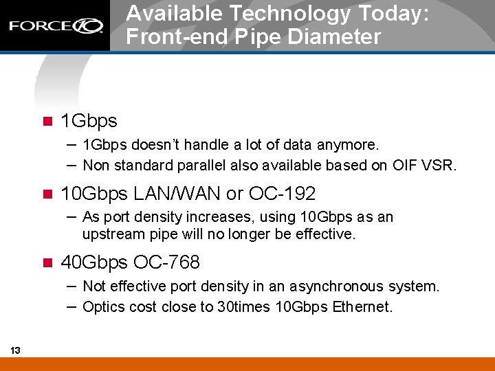
Available Technology Today: Front-end Pipe Diameter n 1 Gbps – 1 Gbps doesn’t handle a lot of data anymore. – Non standard parallel also available based on OIF VSR. n 10 Gbps LAN/WAN or OC-192 – As port density increases, using 10 Gbps as an upstream pipe will no longer be effective. n 40 Gbps OC-768 – Not effective port density in an asynchronous system. – Optics cost close to 30 times 10 Gbps Ethernet. 13
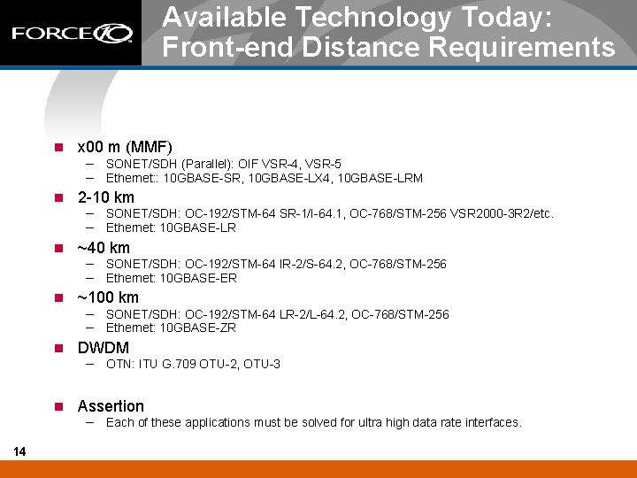
Available Technology Today: Front-end Distance Requirements 14 n x 00 m (MMF) n 2 -10 km n ~40 km n ~100 km n DWDM n Assertion – SONET/SDH (Parallel): OIF VSR-4, VSR-5 – Ethernet: : 10 GBASE-SR, 10 GBASE-LX 4, 10 GBASE-LRM – SONET/SDH: OC-192/STM-64 SR-1/I-64. 1, OC-768/STM-256 VSR 2000 -3 R 2/etc. – Ethernet: 10 GBASE-LR – SONET/SDH: OC-192/STM-64 IR-2/S-64. 2, OC-768/STM-256 – Ethernet: 10 GBASE-ER – SONET/SDH: OC-192/STM-64 LR-2/L-64. 2, OC-768/STM-256 – Ethernet: 10 GBASE-ZR – OTN: ITU G. 709 OTU-2, OTU-3 – Each of these applications must be solved for ultra high data rate interfaces.
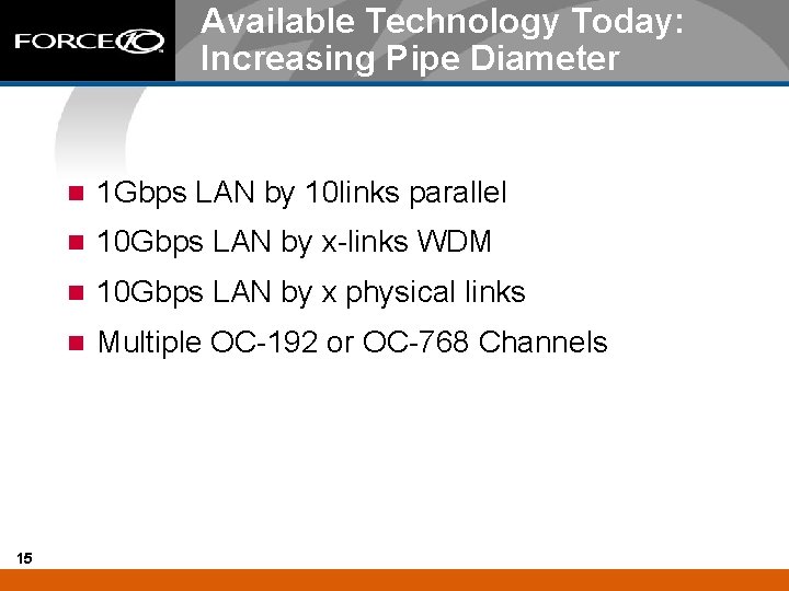
Available Technology Today: Increasing Pipe Diameter 15 n 1 Gbps LAN by 10 links parallel n 10 Gbps LAN by x-links WDM n 10 Gbps LAN by x physical links n Multiple OC-192 or OC-768 Channels
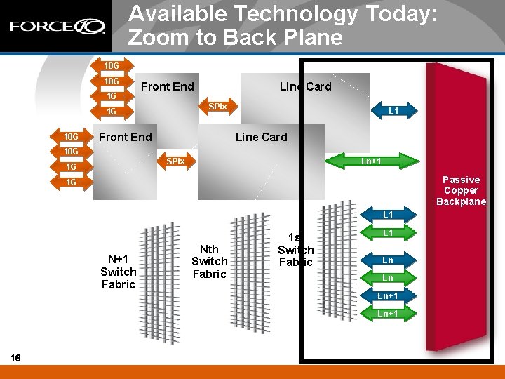
Available Technology Today: Zoom to Back Plane 10 G 1 G Front End SPIx 1 G 10 G Line Card Front End 10 G L 1 SPIx 1 G Ln+1 Passive Copper Backplane 1 G L 1 N+1 Switch Fabric Nth Switch Fabric 1 st Switch Fabric L 1 Ln Ln Ln+1 16
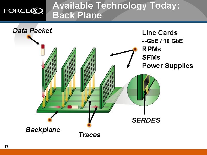
Available Technology Today: Back Plane Data Packet Line Cards --Gb. E / 10 Gb. E RPMs SFMs Power Supplies SERDES Backplane 17 Traces
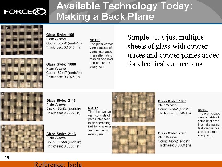
Available Technology Today: Making a Back Plane Simple! It’s just multiple sheets of glass with copper traces and copper planes added for electrical connections. 18
Available Technology Today: Back Plane Pipe Diameter n 1. 25 Gbps – Used in systems with five to ten year old technology. n 2. 5 Gbps/3. 125 Gbps – Used in systems with five year old or less technology. n 5 Gbps/6. 25 Gbps – Used within the last 12 months. 19
Available Technology Today: Increasing Pipe Diameter n Can’t WDM copper n 10. 3 Gbps/12. 5 Gbps – Not largely deployed at this time. n 20 Increasing the pipe diameter on a back plane with assigned slot pins can only be done by changing the glass construction.
Available Technology Today: Pipe Diameter is NOT Flexible n 21 Once the pipe is designed and built to a certain pipe speed, making the pipe faster is extremely difficult, if not impossible.
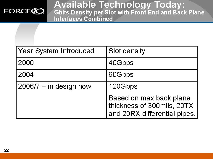
Available Technology Today: Gbits Density per Slot with Front End and Back Plane Interfaces Combined Year System Introduced Slot density 2000 40 Gbps 2004 60 Gbps 2006/7 – in design now 120 Gbps Based on max back plane thickness of 300 mils, 20 TX and 20 RX differential pipes. 22
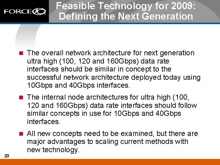
Feasible Technology for 2009: Defining the Next Generation 23 n The overall network architecture for next generation ultra high (100, 120 and 160 Gbps) data rate interfaces should be similar in concept to the successful network architecture deployed today using 10 Gbps and 40 Gbps interfaces. n The internal node architectures for ultra high (100, 120 and 160 Gbps) data rate interfaces should follow similar concepts in use for 10 Gbps and 40 Gbps interfaces. n All new concepts need to be examined, but there are major advantages to scaling current methods with new technology.
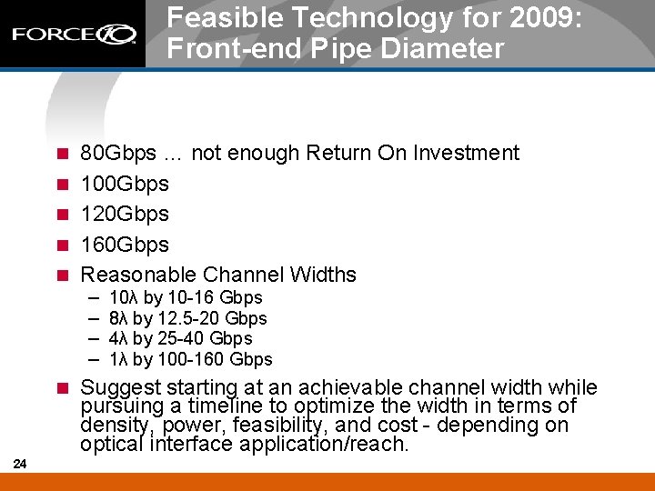
Feasible Technology for 2009: Front-end Pipe Diameter n n n 24 80 Gbps … not enough Return On Investment 100 Gbps 120 Gbps 160 Gbps Reasonable Channel Widths – – 10λ by 10 -16 Gbps 8λ by 12. 5 -20 Gbps 4λ by 25 -40 Gbps 1λ by 100 -160 Gbps Suggest starting at an achievable channel width while pursuing a timeline to optimize the width in terms of density, power, feasibility, and cost - depending on optical interface application/reach.
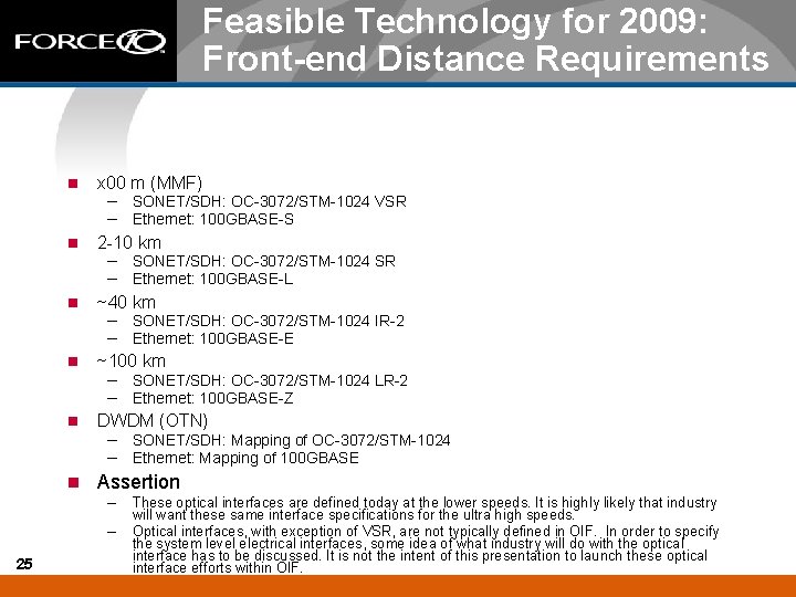
Feasible Technology for 2009: Front-end Distance Requirements n n n x 00 m (MMF) – SONET/SDH: OC-3072/STM-1024 VSR – Ethernet: 100 GBASE-S 2 -10 km – SONET/SDH: OC-3072/STM-1024 SR – Ethernet: 100 GBASE-L ~40 km – SONET/SDH: OC-3072/STM-1024 IR-2 – Ethernet: 100 GBASE-E ~100 km – SONET/SDH: OC-3072/STM-1024 LR-2 – Ethernet: 100 GBASE-Z DWDM (OTN) – SONET/SDH: Mapping of OC-3072/STM-1024 – Ethernet: Mapping of 100 GBASE Assertion – These optical interfaces are defined today at the lower speeds. It is highly likely that industry – 25 will want these same interface specifications for the ultra high speeds. Optical interfaces, with exception of VSR, are not typically defined in OIF. In order to specify the system level electrical interfaces, some idea of what industry will do with the optical interface has to be discussed. It is not the intent of this presentation to launch these optical interface efforts within OIF.
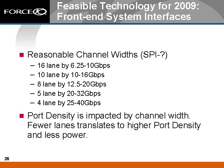
Feasible Technology for 2009: Front-end System Interfaces n Reasonable Channel Widths (SPI-? ) – – – n 26 16 lane by 6. 25 -10 Gbps 10 lane by 10 -16 Gbps 8 lane by 12. 5 -20 Gbps 5 lane by 20 -32 Gbps 4 lane by 25 -40 Gbps Port Density is impacted by channel width. Fewer lanes translates to higher Port Density and less power.
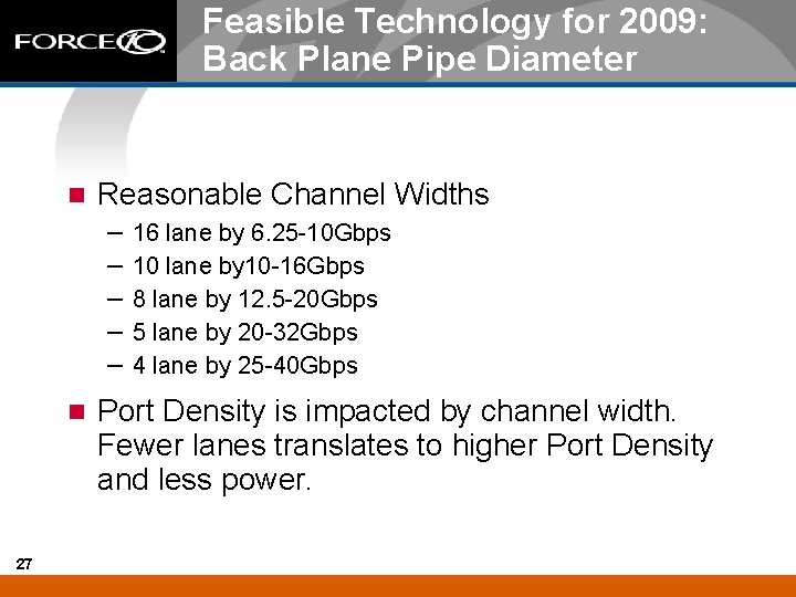
Feasible Technology for 2009: Back Plane Pipe Diameter n Reasonable Channel Widths – – – n 27 16 lane by 6. 25 -10 Gbps 10 lane by 10 -16 Gbps 8 lane by 12. 5 -20 Gbps 5 lane by 20 -32 Gbps 4 lane by 25 -40 Gbps Port Density is impacted by channel width. Fewer lanes translates to higher Port Density and less power.
Feasible Technology for 2009: Pipe Diameter is NOT Flexible n 28 New Back Plane designs will have to have pipes that can handle 20 Gbps to 25 Gbps.
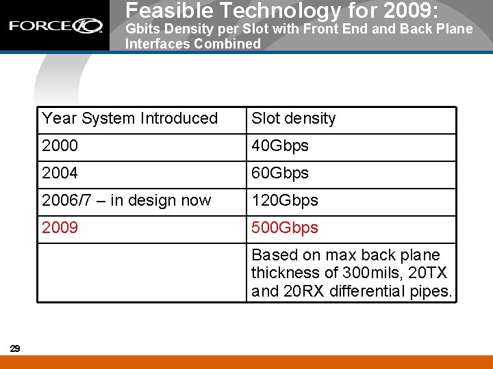
Feasible Technology for 2009: Gbits Density per Slot with Front End and Back Plane Interfaces Combined Year System Introduced Slot density 2000 40 Gbps 2004 60 Gbps 2006/7 – in design now 120 Gbps 2009 500 Gbps Based on max back plane thickness of 300 mils, 20 TX and 20 RX differential pipes. 29
Feasible Technology for 2009: 100 Gbps Options Bit rate shown above is based on 100 Gbps. Scale the bit rate accordingly to achieve 160 Gbps. 30
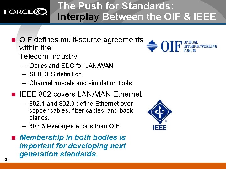
The Push for Standards: Interplay Between the OIF & IEEE n OIF defines multi-source agreements within the Telecom Industry. – Optics and EDC for LAN/WAN – SERDES definition – Channel models and simulation tools n IEEE 802 covers LAN/MAN Ethernet – 802. 1 and 802. 3 define Ethernet over copper cables, fiber cables, and back planes. – 802. 3 leverages efforts from OIF. n 31 Membership in both bodies is important for developing next generation standards.
The Push for Standards: OIF n Force 10 Labs introduced three efforts within OIF to drive 100 Gbps to 160 Gbps connectivity. – Two interfaces for interconnecting optics, ASICs, and backplanes. – A 25 Gbps SERDES – Updates of design criteria to the Systems User Group 32
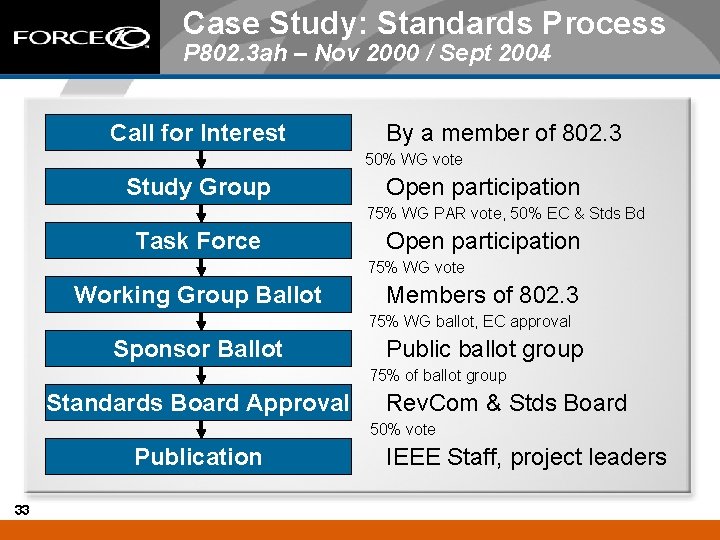
Case Study: Standards Process P 802. 3 ah – Nov 2000 / Sept 2004 Call for Interest By a member of 802. 3 50% WG vote Study Group Open participation 75% WG PAR vote, 50% EC & Stds Bd Task Force Open participation 75% WG vote Working Group Ballot Members of 802. 3 75% WG ballot, EC approval Sponsor Ballot Public ballot group 75% of ballot group Standards Board Approval Rev. Com & Stds Board 50% vote Publication 33 IEEE Staff, project leaders
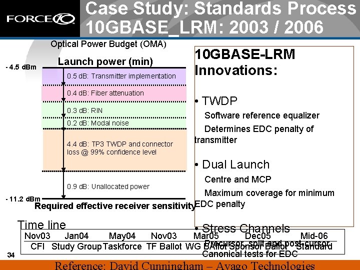
Case Study: Standards Process 10 GBASE_LRM: 2003 / 2006 Optical Power Budget (OMA) - 4. 5 d. Bm Launch power (min) 0. 5 d. B: Transmitter implementation 0. 4 d. B: Fiber attenuation 0. 3 d. B: RIN 0. 2 d. B: Modal noise 4. 4 d. B: TP 3 TWDP and connector loss @ 99% confidence level 10 GBASE-LRM Innovations: • TWDP Software reference equalizer Determines EDC penalty of transmitter • Dual Launch 0. 9 d. B: Unallocated power Centre and MCP Maximum coverage for minimum Required effective receiver sensitivity. EDC penalty - 11. 2 d. Bm Time line 34 • Stress Channels Nov 03 Jan 04 May 04 Nov 03 Mar 05 Dec 05 Mid-06 Precursor, split Ballot and post-cursor CFI Study Group Taskforce TF Ballot WG BAllot Sponsor Standard Canonical tests for EDC
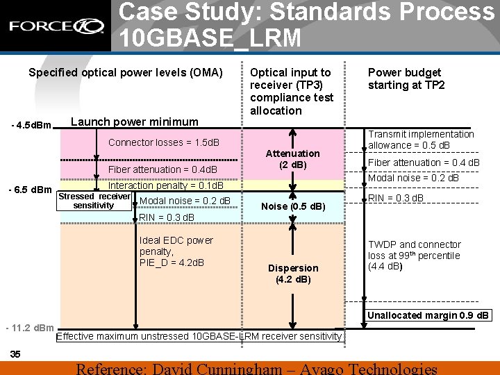
Case Study: Standards Process 10 GBASE_LRM Specified optical power levels (OMA) - 4. 5 d. Bm Launch power minimum Optical input to receiver (TP 3) compliance test allocation Connector losses = 1. 5 d. B Fiber attenuation = 0. 4 d. B - 6. 5 d. Bm Attenuation (2 d. B) Modal noise = 0. 2 d. B Transmit implementation allowance = 0. 5 d. B Fiber attenuation = 0. 4 d. B Modal noise = 0. 2 d. B Interaction penalty = 0. 1 d. B Stressed receiver sensitivity Power budget starting at TP 2 Noise (0. 5 d. B) RIN = 0. 3 d. B Ideal EDC power penalty, PIE_D = 4. 2 d. B Dispersion (4. 2 d. B) TWDP and connector loss at 99 th percentile (4. 4 d. B) Unallocated margin 0. 9 d. B - 11. 2 d. Bm 35 Effective maximum unstressed 10 GBASE-LRM receiver sensitivity
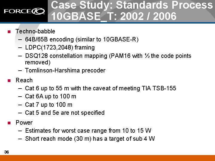
Case Study: Standards Process 10 GBASE_T: 2002 / 2006 n Techno-babble – 64 B/65 B encoding (similar to 10 GBASE-R) – LDPC(1723, 2048) framing – DSQ 128 constellation mapping (PAM 16 with ½ the code points removed) – Tomlinson-Harshima precoder n Reach – Cat 6 up to 55 m with the caveat of meeting TIA TSB-155 – Cat 6 A up to 100 m – Cat 7 up to 100 m – Cat 5 and 5 e are not specified n Power – Estimates for worst case range from 10 to 15 W – Short reach mode (30 m) has a target of sub 4 W 36
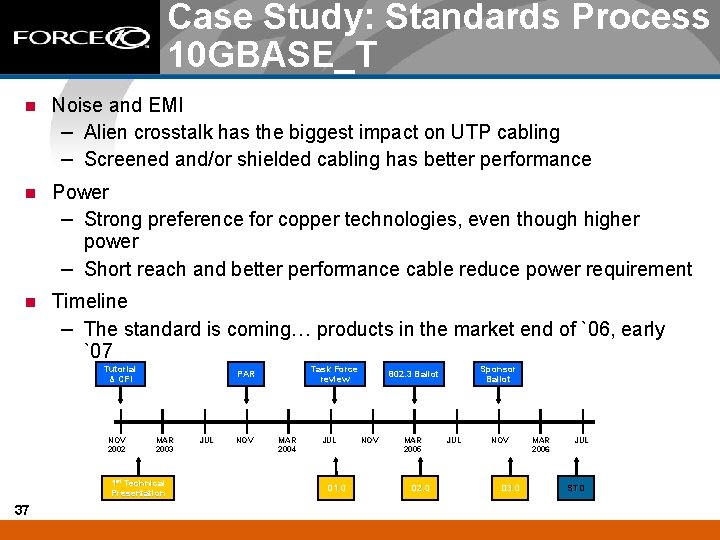
Case Study: Standards Process 10 GBASE_T n Noise and EMI – Alien crosstalk has the biggest impact on UTP cabling – Screened and/or shielded cabling has better performance n Power – Strong preference for copper technologies, even though higher power – Short reach and better performance cable reduce power requirement n Timeline – The standard is coming… products in the market end of `06, early `07 Tutorial & CFI NOV 2002 MAR 2003 1 st Technical Presentation 37 Task Force review PAR JUL NOV MAR 2004 JUL D 1. 0 Sponsor Ballot 802. 3 Ballot NOV MAR 2005 D 2. 0 JUL NOV D 3. 0 MAR 2006 JUL STD

Birth of A Standard It Takes About 5 Years 38 n Ideas from industry n Feasibility and research n Call for Interest (CFI) – 100 Gb. E EFFORT IS HERE n Marketing / Sales potential, technical feasibility n Study Group n Work Group n Drafts n Final member vote
The Push for Standards: IEEE n Force 10 introduces a Call for Interest (CFI) in July 2006 IEEE 802 with Tyco Electronics. – Meetings will be held in the coming months to determine the CFI and the efforts required. – We target July 2006 because of resources within IEEE. – Joel Goergen and John D’Ambrosia will chair the CFI effort. The anchor team is composed of key contributors from Force 10, Tyco, Intel, Quake, and Cisco. It has since broadened to include over 30 companies. 39
The Ethernet Alliance Promoting All Ethernet IEEE Work n Key IEEE 802 Ethernet projects include – – 100 Gb. E Backplane 10 Gb. E LRM / MMF 10 G Base-T n Force 10 is on the Bo. D, principle member n 20 companies at launch – Sun, Intel, Foundry, Broadcam. . . – Now approaching 40 companies 40 n Launch January 10, 2006 n Opportunity for customers to speak on behalf of 100 Gb. E Ethernet
Anatomy of a 100 Gbps Solution: Architectural Disclaimers n There Are Many Ways to Implement a system – This section covers two basic types. – Issues facing 100 Gbps ports are addressed in basic form. n Channel Performance or ‘Pipe Capacity’ is difficult to measure n Two Popular Chassis Heights – 24 in to 34 in Height (2 or 3 Per Rack) – 10 in to 14 in Height (5 to 8 Per Rack) 41
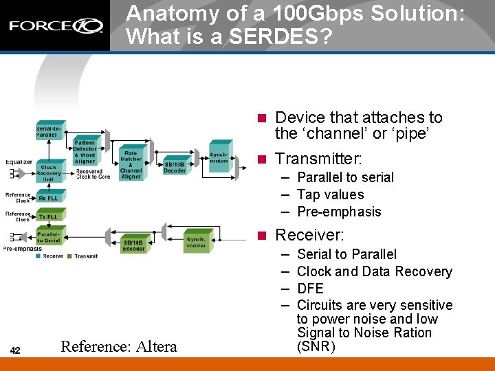
Anatomy of a 100 Gbps Solution: What is a SERDES? n Device that attaches to the ‘channel’ or ‘pipe’ n Transmitter: – Parallel to serial – Tap values – Pre-emphasis n Receiver: – – 42 Reference: Altera Serial to Parallel Clock and Data Recovery DFE Circuits are very sensitive to power noise and low Signal to Noise Ration (SNR)
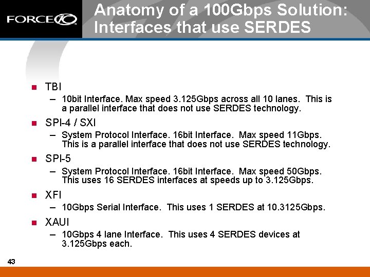
Anatomy of a 100 Gbps Solution: Interfaces that use SERDES n TBI – 10 bit Interface. Max speed 3. 125 Gbps across all 10 lanes. This is a parallel interface that does not use SERDES technology. n SPI-4 / SXI – System Protocol Interface. 16 bit Interface. Max speed 11 Gbps. This is a parallel interface that does not use SERDES technology. n SPI-5 – System Protocol Interface. 16 bit Interface. Max speed 50 Gbps. This uses 16 SERDES interfaces at speeds up to 3. 125 Gbps. XFI – 10 Gbps Serial Interface. This uses 1 SERDES at 10. 3125 Gbps. n XAUI – 10 Gbps 4 lane Interface. This uses 4 SERDES devices at n 3. 125 Gbps each. 43
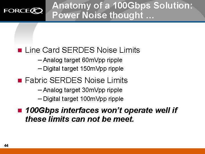
Anatomy of a 100 Gbps Solution: Power Noise thought … n Line Card SERDES Noise Limits – Analog target 60 m. Vpp ripple – Digital target 150 m. Vpp ripple n Fabric SERDES Noise Limits – Analog target 30 m. Vpp ripple – Digital target 100 m. Vpp ripple n 44 100 Gbps interfaces won’t operate well if these limits can not be meet.
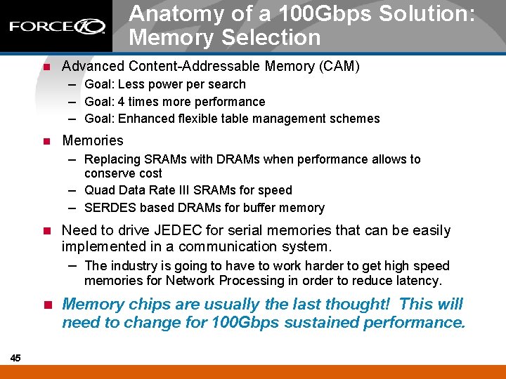
Anatomy of a 100 Gbps Solution: Memory Selection n Advanced Content-Addressable Memory (CAM) – Goal: Less power per search – Goal: 4 times more performance – Goal: Enhanced flexible table management schemes n Memories – Replacing SRAMs with DRAMs when performance allows to conserve cost – Quad Data Rate III SRAMs for speed – SERDES based DRAMs for buffer memory n Need to drive JEDEC for serial memories that can be easily implemented in a communication system. – The industry is going to have to work harder to get high speed memories for Network Processing in order to reduce latency. n 45 Memory chips are usually the last thought! This will need to change for 100 Gbps sustained performance.
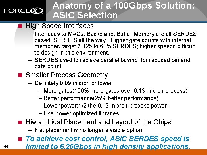
Anatomy of a 100 Gbps Solution: ASIC Selection n High Speed Interfaces – Interfaces to MACs, Backplane, Buffer Memory are all SERDES based. SERDES all the way. Higher gate counts with internal memories target 3. 125 to 6. 25 SERDES; higher speeds difficult to design in this environment. – SERDES used to replace parallel busing for reduced pin and gate count n Smaller Process Geometry – Definitely 0. 09 micron or lower – More gates(100% more gates over 0. 13 micron process) – Better performance(25% better performance) – Lower power(1/2 the 0. 13 micron process power) – Use power optimized libraries n Hierarchical Placement and Layout of the Chips – Flat placement is no longer a viable option n 46 To achieve cost control, ASIC SERDES speed is limited to 6. 25 Gbps in high density applications.
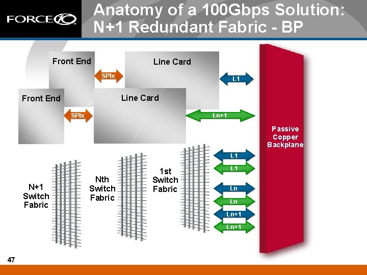
Anatomy of a 100 Gbps Solution: N+1 Redundant Fabric - BP Front End Line Card SPIx L 1 Line Card Front End SPIx Ln+1 Passive Copper Backplane L 1 N+1 Switch Fabric Nth Switch Fabric 1 st Switch Fabric L 1 Ln Ln Ln+1 47
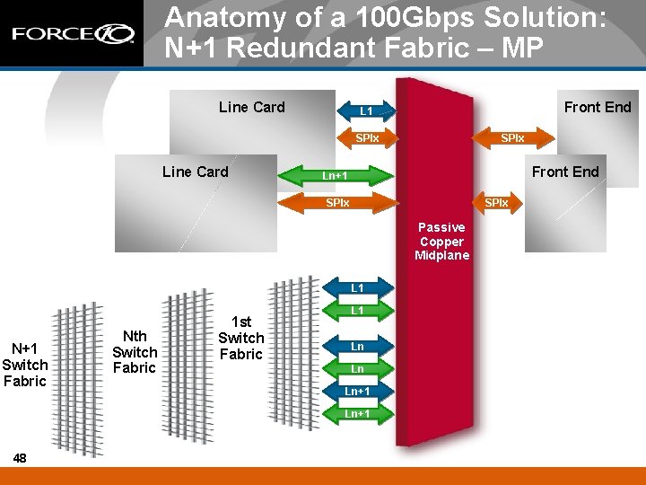
Anatomy of a 100 Gbps Solution: N+1 Redundant Fabric – MP Line Card Front End L 1 SPIx Line Card SPIx Front End Ln+1 SPIx Passive Copper Midplane L 1 N+1 Switch Fabric Nth Switch Fabric 1 st Switch Fabric L 1 Ln Ln Ln+1 48
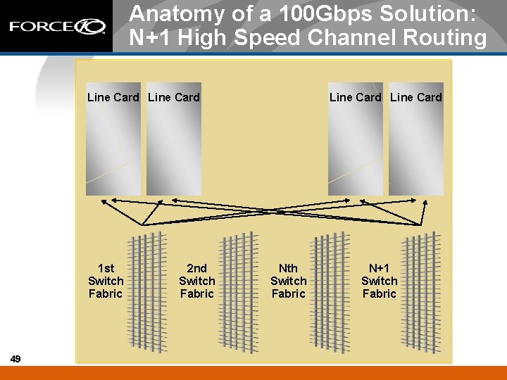
Anatomy of a 100 Gbps Solution: N+1 High Speed Channel Routing Line Card 1 st Switch Fabric 49 2 nd Switch Fabric Line Card Nth Switch Fabric N+1 Switch Fabric
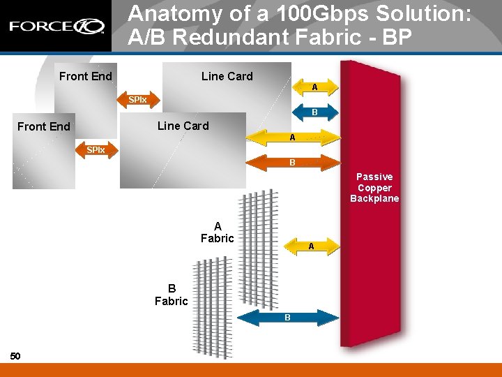
Anatomy of a 100 Gbps Solution: A/B Redundant Fabric - BP Front End Line Card A SPIx B Line Card Front End A SPIx B Passive Copper Backplane A Fabric A B Fabric B 50
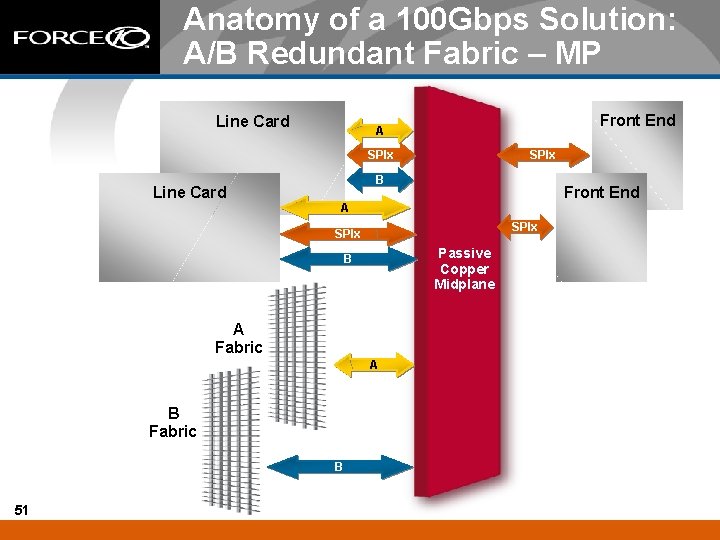
Anatomy of a 100 Gbps Solution: A/B Redundant Fabric – MP Line Card Front End A SPIx Line Card SPIx B Front End A SPIx Passive Copper Midplane B A Fabric A B Fabric B 51
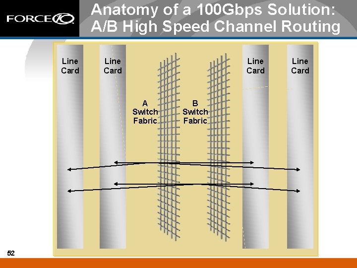
Anatomy of a 100 Gbps Solution: A/B High Speed Channel Routing Line Card A Switch Fabric 52 B Switch Fabric Line Card
Anatomy of a 100 Gbps Solution: A Quick Thought …. . n Looking at both Routing and Connector Complexity designed into the differential signaling …. – Best Case: N+1 Fabric in a Back Plane. – Worst Case: A/B Fabric in a Mid Plane. n 53 All implementations need to be examined for best possible performance over all deployed network interfaces. Manufacturability and channel (Pipe) noise are two of the bigger factors.
Anatomy of a 100 Gbps Solution: Determine Trace Lengths n After careful review of possible Line Card, Switch Fabric, and Back Plane Architectural blocks, determine the range of trace lengths that exist between a SERDES transmitter and a SERDES receiver. 30 inches or. 75 meters total should do it. n Several factors stem from trace length. – – – n 54 Band Width Reflections from via and or thru-holes Circuit board material BER Coding Keep in mind that the goal is to target one or both basic chassis dimensions.
Anatomy of a 100 Gbps Solution: Channel Model Description n A “Channel” or “Pipe” is a high speed singleended or differential signal connecting the SERDES transmitter to the SERDES receiver. The context of “Channel” or “Pipe” from this point is considered differential. n Develop a channel model based on the implications of Architectural choices and trace lengths. – – 55 Identifies a clean launch route to a BGA device. Identifies design constraints and concerns. Includes practical recommendations. Identifies channel Bandwidth.
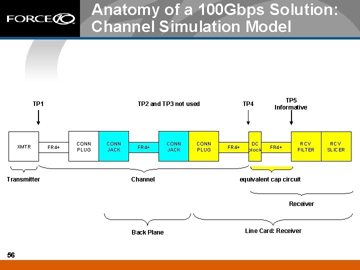
Anatomy of a 100 Gbps Solution: Channel Simulation Model TP 1 XMTR Transmitter TP 4 TP 2 and TP 3 not used FR 4+ CONN PLUG CONN JACK FR 4+ Channel CONN JACK CONN PLUG FR 4+ DC block TP 5 Informative FR 4+ RCV FILTER equivalent cap circuit Receiver Back Plane 56 Line Card: Receiver RCV SLICER
Anatomy of a 100 Gbps Solution: Channel: Back Plane n 57 Shows signal trace connecting pins on separate connectors across a back plane.
Anatomy of a 100 Gbps Solution: Channel: Line Card Receiver n 58 Shows a signal trace connecting the back plane to a SERDES in a Ball Grid Array (BGA) package.
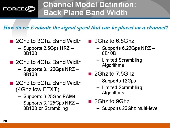
Channel Model Definition: Back Plane Band Width How do we Evaluate the signal speed that can be placed on a channel? n 2 Ghz to 3 Ghz Band Width n – Supports 2. 5 Gps NRZ – – Supports 6. 25 Gps NRZ – 8 B 10 B n n 8 B 10 B or Scrambling 2 Ghz to 7. 5 Ghz – Supports 12 Gps – Limited Scrambling 2 Ghz to 5 Ghz Band Width (4 Ghz low FEXT) – Supports 6. 25 Gps PAM 4 – Supports 3. 125 Gps NRZ – 59 8 B 10 B – Limited Scrambling Algorithms 2 Ghz to 4 Ghz Band Width – Supports 3. 125 Gps NRZ – 2 Ghz to 6. 5 Ghz Algorithms n 2 Ghz to 9 Ghz – Supports 25 Ghz multi-level
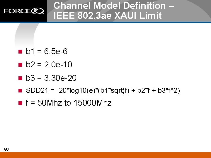
Channel Model Definition – IEEE 802. 3 ae XAUI Limit 60 n b 1 = 6. 5 e-6 n b 2 = 2. 0 e-10 n b 3 = 3. 30 e-20 n SDD 21 = -20*log 10(e)*(b 1*sqrt(f) + b 2*f + b 3*f^2) n f = 50 Mhz to 15000 Mhz
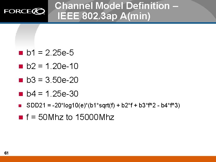
Channel Model Definition – IEEE 802. 3 ap A(min) 61 n b 1 = 2. 25 e-5 n b 2 = 1. 20 e-10 n b 3 = 3. 50 e-20 n b 4 = 1. 25 e-30 n SDD 21 = -20*log 10(e)*(b 1*sqrt(f) + b 2*f + b 3*f^2 - b 4*f^3) n f = 50 Mhz to 15000 Mhz
Anatomy of a 100 Gbps Solution: Channel Model Limit Lines 62
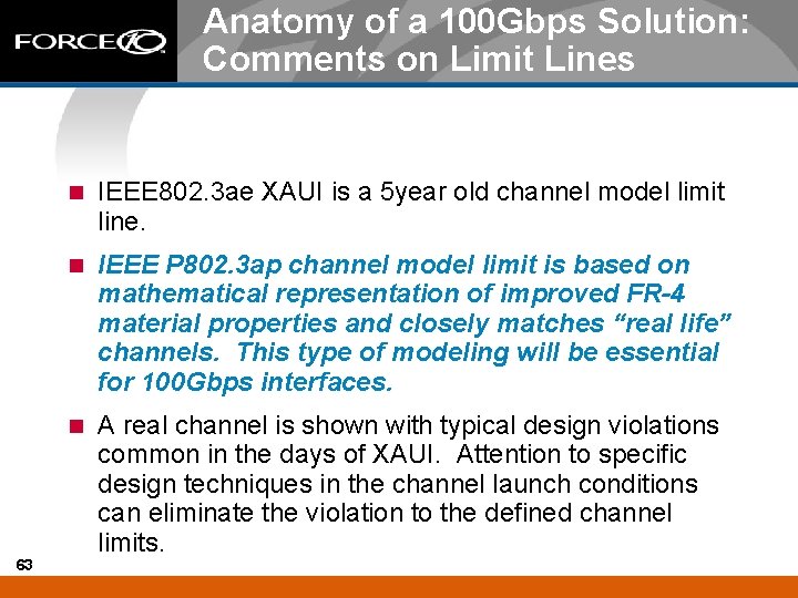
Anatomy of a 100 Gbps Solution: Comments on Limit Lines 63 n IEEE 802. 3 ae XAUI is a 5 year old channel model limit line. n IEEE P 802. 3 ap channel model limit is based on mathematical representation of improved FR-4 material properties and closely matches “real life” channels. This type of modeling will be essential for 100 Gbps interfaces. n A real channel is shown with typical design violations common in the days of XAUI. Attention to specific design techniques in the channel launch conditions can eliminate the violation to the defined channel limits.
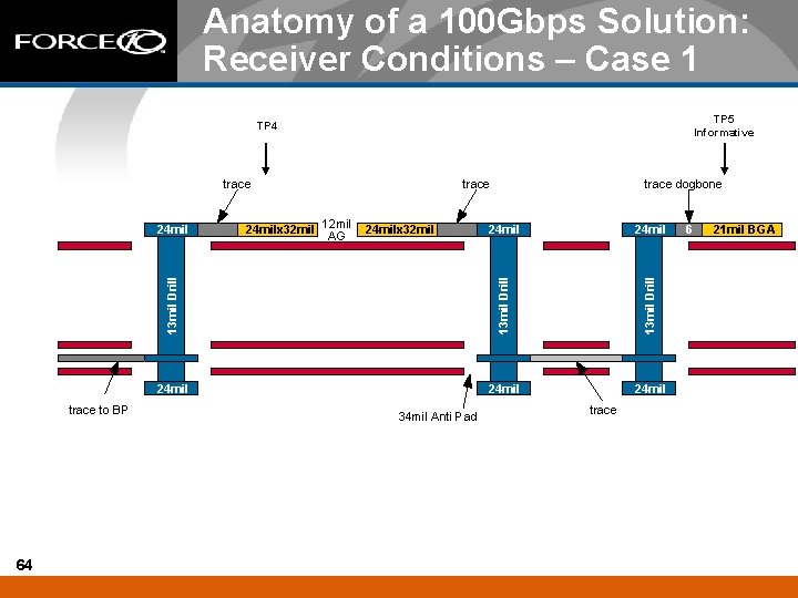
Anatomy of a 100 Gbps Solution: Receiver Conditions – Case 1 TP 5 Informative TP 4 trace to BP 64 24 mil 13 mil Drill 24 milx 32 mil 12 mil AG trace dogbone 13 mil Drill 24 mil trace 24 mil 34 mil Anti Pad trace 6 21 mil BGA
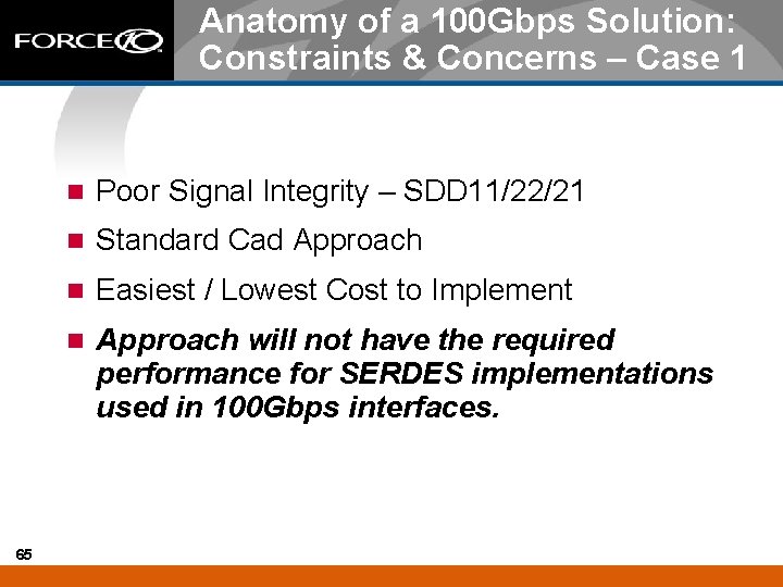
Anatomy of a 100 Gbps Solution: Constraints & Concerns – Case 1 65 n Poor Signal Integrity – SDD 11/22/21 n Standard Cad Approach n Easiest / Lowest Cost to Implement n Approach will not have the required performance for SERDES implementations used in 100 Gbps interfaces.
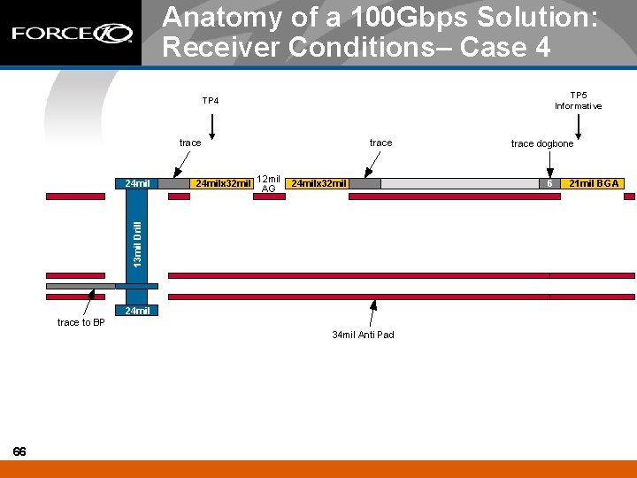
Anatomy of a 100 Gbps Solution: Receiver Conditions– Case 4 TP 5 Informative TP 4 trace 24 milx 32 mil 12 mil AG 24 milx 32 mil 13 mil Drill 24 mil trace to BP 34 mil Anti Pad 66 trace dogbone 6 21 mil BGA
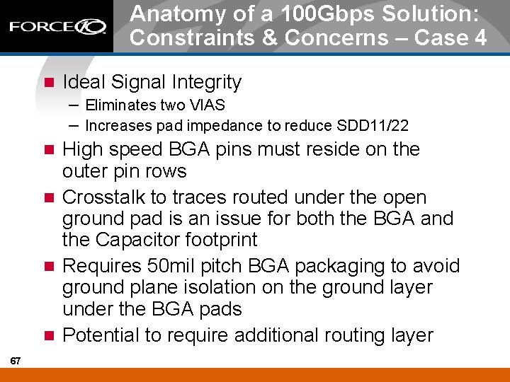
Anatomy of a 100 Gbps Solution: Constraints & Concerns – Case 4 n Ideal Signal Integrity – Eliminates two VIAS – Increases pad impedance to reduce SDD 11/22 High speed BGA pins must reside on the outer pin rows n Crosstalk to traces routed under the open ground pad is an issue for both the BGA and the Capacitor footprint n Requires 50 mil pitch BGA packaging to avoid ground plane isolation on the ground layer under the BGA pads n Potential to require additional routing layer n 67
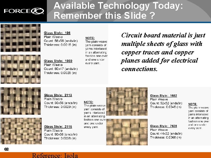
Available Technology Today: Remember this Slide ? Circuit board material is just multiple sheets of glass with copper traces and copper planes added for electrical connections. 68
Anatomy of a 100 Gbps Solution: Channel Design Considerations n Circuit Board Material Selection is Based on the Following: – Temperature and Humidity effects on Df (Dissipation – – – 69 Factor) and Dk (Dielectric Constant) Required mounting holes for mother-card mounting, shock and vibration Required number of times a chip or connector can be replaced Required number of times a pin can be replaced on a back plane Aspect ratio (Drilled hole size to board thickness) Power plane copper weight Coding / Signaling scheme
Anatomy of a 100 Gbps Solution: Materials in Perspective Graph 70 provided by Zhi Wong zwong@altera. com
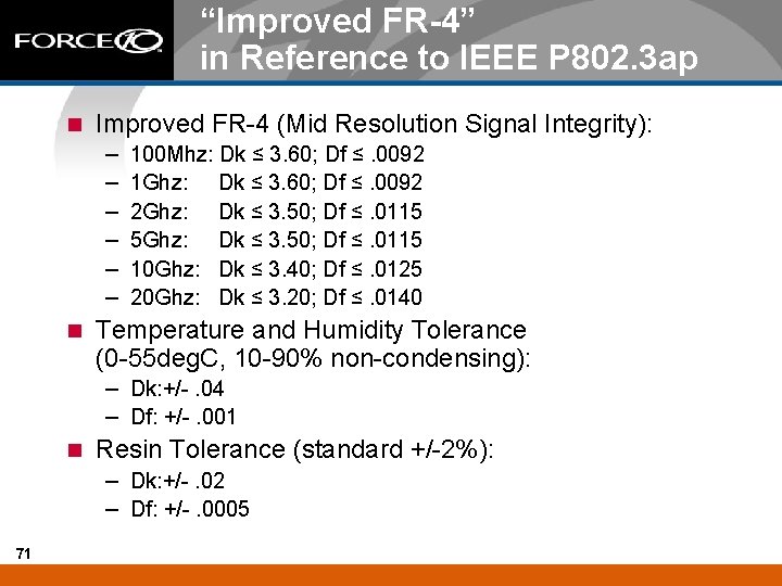
“Improved FR-4” in Reference to IEEE P 802. 3 ap n Improved FR-4 (Mid Resolution Signal Integrity): – – – n 100 Mhz: Dk ≤ 3. 60; Df ≤. 0092 1 Ghz: Dk ≤ 3. 60; Df ≤. 0092 2 Ghz: Dk ≤ 3. 50; Df ≤. 0115 5 Ghz: Dk ≤ 3. 50; Df ≤. 0115 10 Ghz: Dk ≤ 3. 40; Df ≤. 0125 20 Ghz: Dk ≤ 3. 20; Df ≤. 0140 Temperature and Humidity Tolerance (0 -55 deg. C, 10 -90% non-condensing): – Dk: +/-. 04 – Df: +/-. 001 n Resin Tolerance (standard +/-2%): – Dk: +/-. 02 – Df: +/-. 0005 71
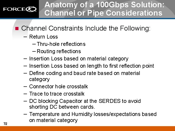
Anatomy of a 100 Gbps Solution: Channel or Pipe Considerations n Channel Constraints Include the Following: – Return Loss – Thru-hole reflections – Routing reflections – Insertion Loss based on material category – Insertion Loss based on length to first reflection point – Define coding and baud rate based on material – – 72 category Connector hole crosstalk Trace to trace crosstalk DC blocking Capacitor at the SERDES to avoid shorting DC between cards. Temperature and Humidity losses/expectations based on material category
Channel Model Starting Point: Materials in Perspective Target Area Graph 73 provided by Zhi Wong zwong@altera. com
Channel Model Starting Point: Real Channels 74
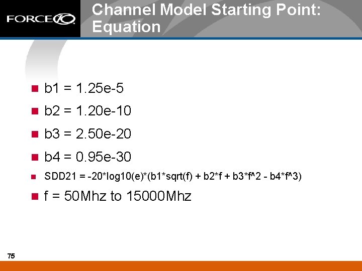
Channel Model Starting Point: Equation 75 n b 1 = 1. 25 e-5 n b 2 = 1. 20 e-10 n b 3 = 2. 50 e-20 n b 4 = 0. 95 e-30 n SDD 21 = -20*log 10(e)*(b 1*sqrt(f) + b 2*f + b 3*f^2 - b 4*f^3) n f = 50 Mhz to 15000 Mhz
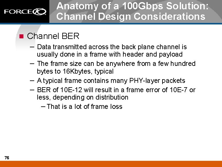
Anatomy of a 100 Gbps Solution: Channel Design Considerations n Channel BER – Data transmitted across the back plane channel is usually done in a frame with header and payload – The frame size can be anywhere from a few hundred bytes to 16 Kbytes, typical – A typical frame contains many PHY-layer packets – BER of 10 E-12 will result in a frame error of 10 E-7 or less, depending on distribution – That is a lot of frame loss 76
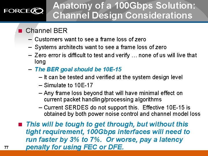
Anatomy of a 100 Gbps Solution: Channel Design Considerations n Channel BER – Customers want to see a frame loss of zero – Systems architects want to see a frame loss of zero – Zero error is difficult to test and verify … none of us will live that long – The BER goal should be 10 E-15 – It can be tested and verified at the system design level – Simulate to 10 E-17 – Any frame loss beyond that will have minimal effect on current packet handling/processing algorithms – Current SERDES do not support this. Effective 10 E-15 is obtained by both power noise control and channel model loss n 77 This will be tough to get through, but without this tight requirement, 100 Gbps interfaces will need to run faster by 3% to 7%. Or worse, pay a latency penalty for using FEC or DFE.
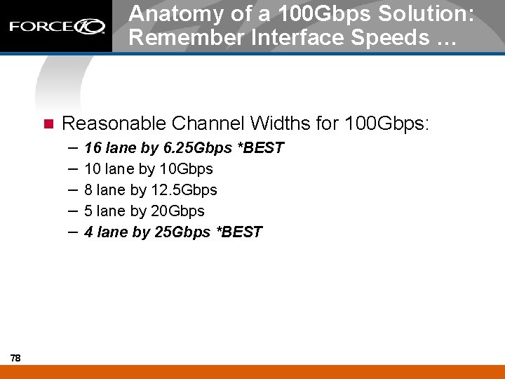
Anatomy of a 100 Gbps Solution: Remember Interface Speeds … n Reasonable Channel Widths for 100 Gbps: – – – 78 16 lane by 6. 25 Gbps *BEST 10 lane by 10 Gbps 8 lane by 12. 5 Gbps 5 lane by 20 Gbps 4 lane by 25 Gbps *BEST
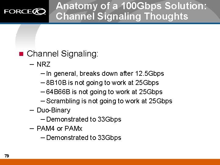
Anatomy of a 100 Gbps Solution: Channel Signaling Thoughts n Channel Signaling: – NRZ – In general, breaks down after 12. 5 Gbps – 8 B 10 B is not going to work at 25 Gbps – 64 B 66 B is not going to work at 25 Gbps – Scrambling is not going to work at 25 Gbps – Duo-Binary – Demonstrated to 33 Gbps – PAM 4 or PAMx – Demonstrated to 33 Gbps 79
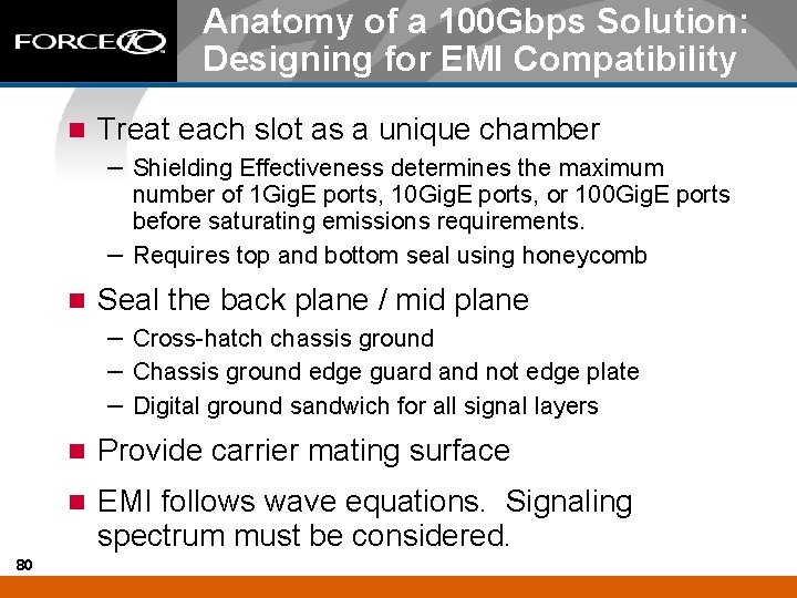
Anatomy of a 100 Gbps Solution: Designing for EMI Compatibility n Treat each slot as a unique chamber – Shielding Effectiveness determines the maximum number of 1 Gig. E ports, 10 Gig. E ports, or 100 Gig. E ports before saturating emissions requirements. – Requires top and bottom seal using honeycomb n Seal the back plane / mid plane – Cross-hatch chassis ground – Chassis ground edge guard and not edge plate – Digital ground sandwich for all signal layers 80 n Provide carrier mating surface n EMI follows wave equations. Signaling spectrum must be considered.
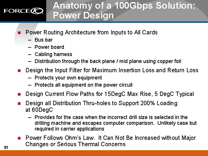
Anatomy of a 100 Gbps Solution: Power Design n Power Routing Architecture from Inputs to All Cards – Bus bar – Power board – Cabling harness – Distribution through the back plane / mid plane using copper foil n Design the Input Filter for Maximum Insertion Loss and Return Loss – Protects your own equipment – Protects all equipment on the power circuit n Design Current Flow Paths for 15 Deg. C Max Rise, 5 Deg. C Typical n Design all Distribution Thru-holes to Support 200% Loading at 60 Deg. C – Provides for the case when the incorrect drill size is selected in the drilling machine and escapes computer comparison. Unlikely case but required in carrier applications n 81 Power Follows Ohm’s Law. It Can Not Be Increased without Major Changes or Serious Thermal Concerns
Summary 82 n Industry has been successful scaling speed since 10 Mbps in 1983. n The efforts in 1 Gig. E and 10 Gig. E have taught us many aspects of interfaces and interface technology. n 100 Gbps and 160 Gbps success will depend on useable chip and optics interfaces. n Significant effort is underway in both IEEE and OIF to define and invent interface to support the next generation speeds. n Systems designers will need to address many new issues to support 100 Gbps port densities of 56 or more per box.
Thank You 83
Backup Slides n 84 The following slides provide additional detail to support information provided within the base presentation.
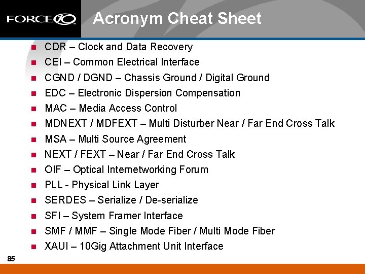
Acronym Cheat Sheet 85 n CDR – Clock and Data Recovery n CEI – Common Electrical Interface n CGND / DGND – Chassis Ground / Digital Ground n EDC – Electronic Dispersion Compensation n MAC – Media Access Control n MDNEXT / MDFEXT – Multi Disturber Near / Far End Cross Talk n MSA – Multi Source Agreement n NEXT / FEXT – Near / Far End Cross Talk n OIF – Optical Internetworking Forum n PLL - Physical Link Layer n SERDES – Serialize / De-serialize n SFI – System Framer Interface n SMF / MMF – Single Mode Fiber / Multi Mode Fiber n XAUI – 10 Gig Attachment Unit Interface
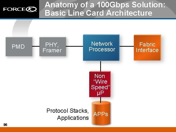
Anatomy of a 100 Gbps Solution: Basic Line Card Architecture PMD PHY, Framer Network Processor Non “Wire Speed” µP Protocol Stacks, APPs Applications 86 Fabric Interface
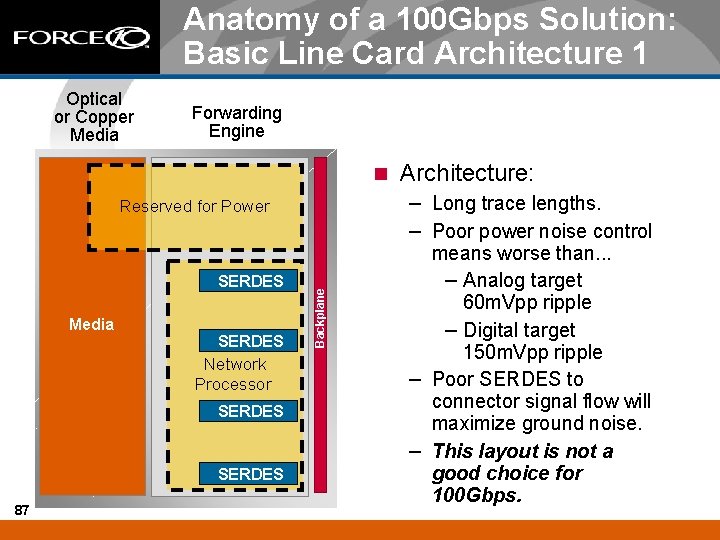
Anatomy of a 100 Gbps Solution: Basic Line Card Architecture 1 Optical or Copper Media Forwarding Engine n – Long trace lengths. – Poor power noise control Media SERDES Network Processor SERDES 87 Backplane Reserved for Power SERDES Architecture: means worse than. . . – Analog target 60 m. Vpp ripple – Digital target 150 m. Vpp ripple – Poor SERDES to connector signal flow will maximize ground noise. – This layout is not a good choice for 100 Gbps.
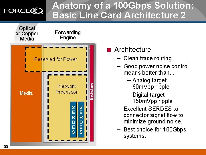
Anatomy of a 100 Gbps Solution: Basic Line Card Architecture 2 Optical or Copper Media Forwarding Engine n – Clean trace routing. – Good power noise control Network Processor S E R D E S 88 Backplane Reserved for Power Media Architecture: S E R D E S means better than. . . – Analog target 60 m. Vpp ripple – Digital target 150 m. Vpp ripple – Excellent SERDES to connector signal flow to minimize ground noise. – Best choice for 100 Gbps systems.
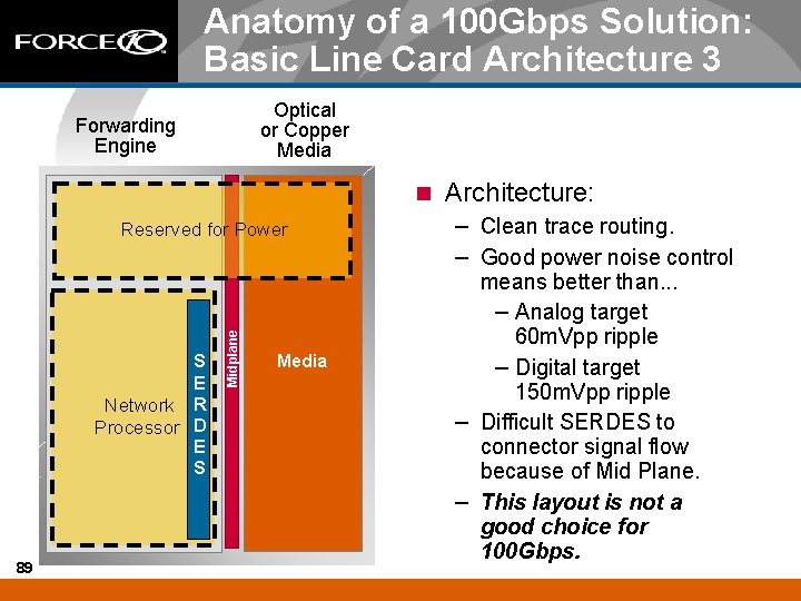
Anatomy of a 100 Gbps Solution: Basic Line Card Architecture 3 Optical or Copper Media Forwarding Engine n S E Network R Processor D E S 89 Midplane Reserved for Power Media Architecture: – Clean trace routing. – Good power noise control means better than. . . – Analog target 60 m. Vpp ripple – Digital target 150 m. Vpp ripple – Difficult SERDES to connector signal flow because of Mid Plane. – This layout is not a good choice for 100 Gbps.
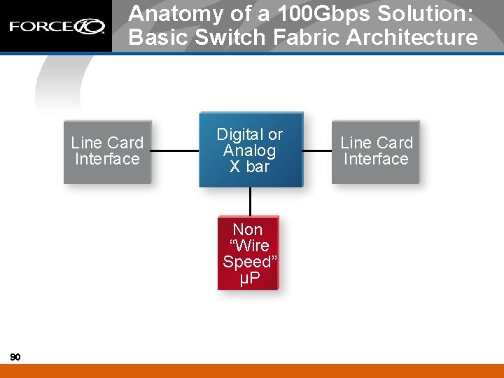
Anatomy of a 100 Gbps Solution: Basic Switch Fabric Architecture Line Card Interface Digital or Analog X bar Non “Wire Speed” µP 90 Line Card Interface
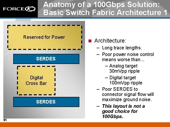
Anatomy of a 100 Gbps Solution: Basic Switch Fabric Architecture 1 Reserved for Power SERDES Digital Cross Bar SERDES 91 n Architecture: – Long trace lengths. – Poor power noise control means worse than. . . – Analog target 30 m. Vpp ripple – Digital target 100 m. Vpp ripple – Poor SERDES to connector signal flow will maximize ground noise. – This layout is not a good choice for 100 Gbps.
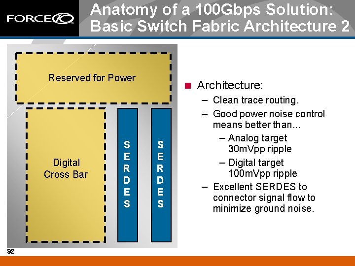
Anatomy of a 100 Gbps Solution: Basic Switch Fabric Architecture 2 Reserved for Power n Architecture: – Clean trace routing. – Good power noise control Digital Cross Bar 92 S E R D E S means better than. . . – Analog target 30 m. Vpp ripple – Digital target 100 m. Vpp ripple – Excellent SERDES to connector signal flow to minimize ground noise.
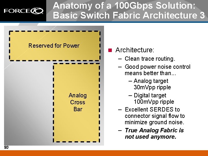
Anatomy of a 100 Gbps Solution: Basic Switch Fabric Architecture 3 Reserved for Power n Architecture: – Clean trace routing. – Good power noise control Analog Cross Bar 93 means better than. . . – Analog target 30 m. Vpp ripple – Digital target 100 m. Vpp ripple – Excellent SERDES to connector signal flow to minimize ground noise. – True Analog Fabric is not used anymore.
Anatomy of a 100 Gbps Solution: Back Plane or Mid Plane n Redundancy – N+1 Fabric – A / B Fabric n Connections – Back Plane – Mid Plane 94
Anatomy of a 100 Gbps Solution: Trace Length Combinations - Max n 95 24 in to 34 in height (2 or 3 per rack)
Anatomy of a 100 Gbps Solution: Trace Length Combinations - Min n 96 24 in to 34 in height (2 or 3 per rack)
Anatomy of a 100 Gbps Solution: Trace Length Combinations - Max n 97 10 in to 14 in height (5 to 8 per rack)
Anatomy of a 100 Gbps Solution: Trace Length Combinations - Min n 98 10 in to 14 in height (5 to 8 per rack)
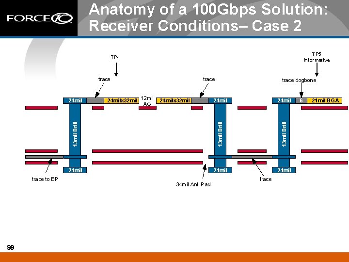
Anatomy of a 100 Gbps Solution: Receiver Conditions– Case 2 TP 5 Informative TP 4 trace to BP 99 24 mil 13 mil Drill 24 milx 32 mil 12 mil AG trace dogbone 13 mil Drill 24 mil trace 24 mil 34 mil Anti Pad trace 6 21 mil BGA
Anatomy of a 100 Gbps Solution: Constraints & Concerns – Case 2 100 n Crosstalk to Traces Routed Under the Open Ground Pad is an Issue n Allows Good Pin Escape from the BGA n Poor Signal Integrity - Has High SDD 11/22/21 at the BGA n Potential to Require Additional Routing Layer n Approach will not have the required performance for SERDES implementations used in 100 Gbps interfaces.
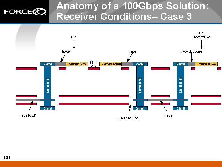
Anatomy of a 100 Gbps Solution: Receiver Conditions– Case 3 TP 5 Informative TP 4 trace to BP 101 24 mil 13 mil Drill 24 milx 32 mil 12 mil AG 13 mil Drill 24 mil trace dogbone trace 24 mil 34 mil Anti Pad trace 6 21 mil BGA
Anatomy of a 100 Gbps Solution: Constraints & Concerns – Case 3 n Allows for Inner High Speed Pad Usage within the BGA n Medium Poor Signal Integrity – SDD 11/22/21. Has the Extra VIAS to Content with in the Break Out – Increases pad impedance to reduce SDD 11/22 102 n Crosstalk to Traces Routed Under the Open Ground Pad is an Issue for Both the BGA and the Capacitor Footprint n Allows Good Pin Escape from the BGA n Potential to Require Additional Routing Layer n Requires 50 mil Pitch BGA Packaging to Avoid Ground Plane Isolation on the Ground Layer Under the BGA Pads
Anatomy of a 100 Gbps Solution: Stack-up Detail 103
Requirements to Consider when Increasing Channel Speed 104 n Signaling Scheme vs Available Bandwidth n NEXT/FEXT Margins n Average Power Noise as Seen by the Receive Slicing Circuit and the PLL n Insertion Loss (SDD 21) Limits
- Slides: 104