Programmable Logic System Design Lab 03 Simulation Preliminary

Programmable Logic System Design Lab 03 - Simulation Preliminary SOC LAB. 2019. 10. 17

Altera Cyclone II DE 2 -70 FPGA board

Create Xilinx Project o 若忘記 Quartus II 開新 Project 的設定請參考 Lab 1 的講義

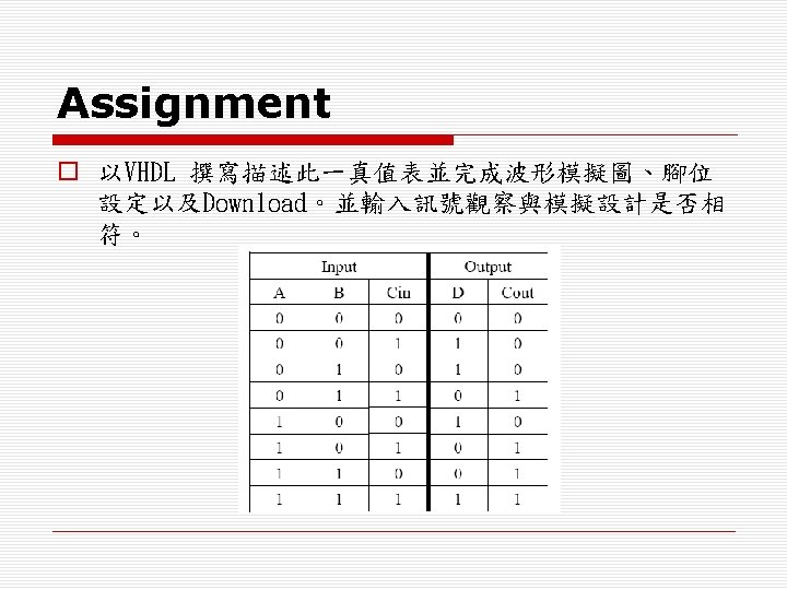
Use Switches to Light LEDs library IEEE; use IEEE. STD_LOGIC_1164. ALL; use IEEE. STD_LOGIC_ARITH. ALL; use IEEE. STD_LOGIC_UNSIGNED. ALL; entity lab 3 is Port ( i. SW : in std_logic_vector(9 downto 0); o. LEDR : out std_logic_vector(9 downto 0)); end lab 3; architecture Behavioral of lab 3 is begin o. LEDR(9 downto 0) <= i. SW(9 downto 0); end Behavioral;

Pin Assignment o Open Pin planner
 o Check pin assignment")
Pin Assignment (Cont’d) o Check pin assignment

Programming Process

Program the DE 1 -SOC Board
 o Open Hardware Setup")
Program the DE 1 -SOC Board(Cont’d) o Open Hardware Setup
![Program the DE 1 -SOC Board(Cont’d) o Select hardware as USB-Blaster [USB-0]](http://slidetodoc.com/presentation_image/1f5e73a33a44776f26f28aed8b2938d7/image-12.jpg "Program the DE 1 -SOC Board(Cont’d) o Select hardware as USB-Blaster [USB-0]")
Program the DE 1 -SOC Board(Cont’d) o Select hardware as USB-Blaster [USB-0]
 o Select auto Detect")
Program the DE 1 -SOC Board(Cont’d) o Select auto Detect
 o Change file")
Program the DE 1 -SOC Board(Cont’d) o Change file
 o Select your file (*. sof )")
Program the DE 1 -SOC Board(Cont’d) o Select your file (*. sof )
 o Start program")
Program the DE 1 -SOC Board(Cont’d) o Start program
 o Program success")
Program the DE 1 -SOC Board(Cont’d) o Program success

CONNECT THE USB CABLE BETWEEN THE COMPUTER AND FPGA BOARD

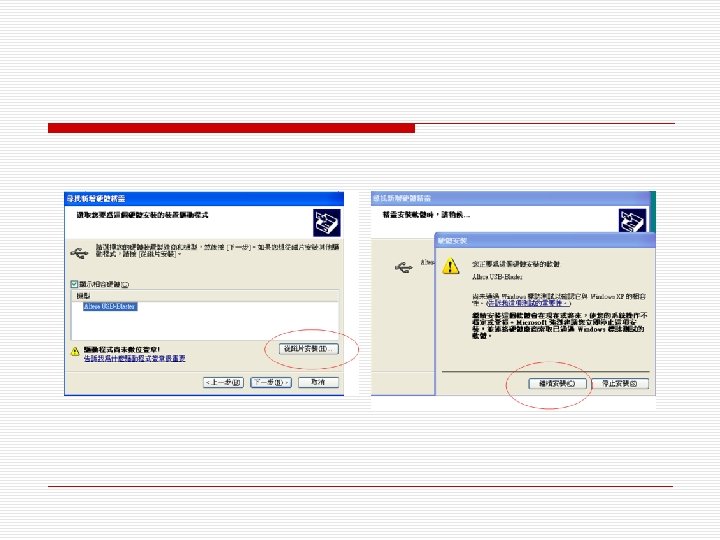
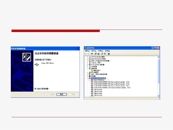
o Right click “USB-Blaster” and select setup driver. Then select “install from a list or specific location”.
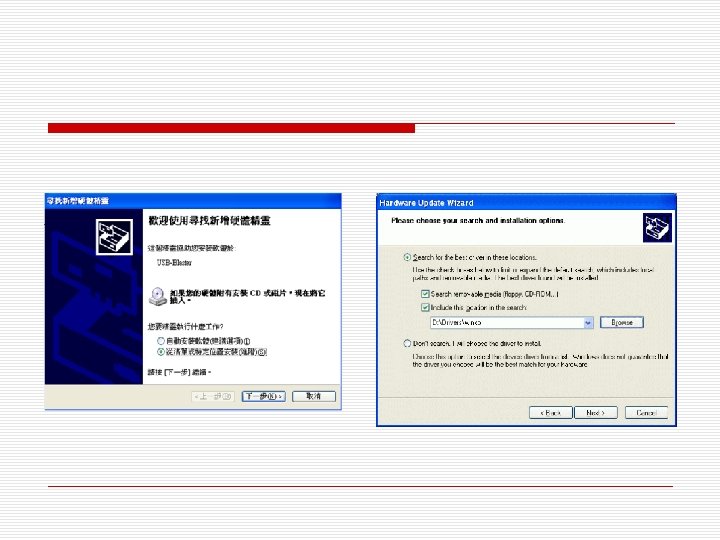

o Choose the file from C: altera13. 0 sp 1quartusdriversusbblaster and install.
- Slides: 24