Programmable Logic Device Architectures WenHung Liao Ph D

Programmable Logic Device Architectures Wen-Hung Liao, Ph. D.
Outline l l l l Digital systems family tree Fundamentals of PLD circuitry PLD architecture The GAL 16 V 8 The Altera EPM 7128 S CPLD The Altera FLEX 10 K Family The Altera Cyclone Family
Objectives l l l l Describe the different categories of digital system devices Describe the different types of PLDs. Interpret PLD data book information. Define PLD terminology Compare the different programming technologies used in PLDs. Compare the architectures of different types of PLDs. Compare the feature of the Altera MAX 70000 S and FLEX 10 K families of PLDs.
Introduction l l We have learned how the building blocks of digital systems work and combine them to solve a wide variety of digital problems. Instead of simple gates or MSI-type ICs, programmable logic devices (PLDs) are being used to implement digital systems.
Why PLD? l l With programmable devices, the same functionality can be obtained with one IC rather than using several individual logic chips. Less board space, less power required, greater reliability, less inventory, and overall lower cost in manufacturing.
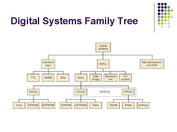
Digital Systems Family Tree
Three Major Categories l l l Standard logic: TTL, CMOS, ECL families. Application specific integrated circuits (ASICs): PLDS, gate arrays, standard cell, full custom. Microprocessors and digital signal processors (DSP): great flexibility, but slower. Using a hardware solution for your digital system design is always faster than a software solution.
Programmable Logic Devices l Programmable logic devices: (do not need to contract with an IC foundry to fabricate) l l Simple PLDs (SPLDs) Complex PLDS (CPLDs) Filed programmable gate arrays (FPGAs) CLPDs and FPGAs are often referred to as high-capacity programmable logic devices (HCPLDs).
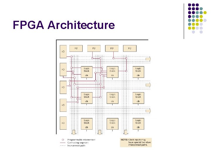
FPGA Architecture
Gate Array l l l ULSI circuits that offers hundreds of thousands of gates. The desired logic functions are created by interconnections of these prefabricated gates. A custom-designed mask for the specific application determines the gate interconnection. (MPGAs).
Standard-cell ASICs l l Use predefined logic function building blocks called cells to create the desired digital systems. IC layout of each cell has been designed previously. A library of available cell is stored in a computer database. The needed cells are laid out for the desired application, and the interconnections between the cells are determined.
Full-custom ASICs: l l All components and the interconnections between them are custom-designed by the IC designed. Higher design cost, but can operate at highest possible speed and require smallest die.
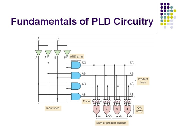
Fundamentals of PLD Circuitry
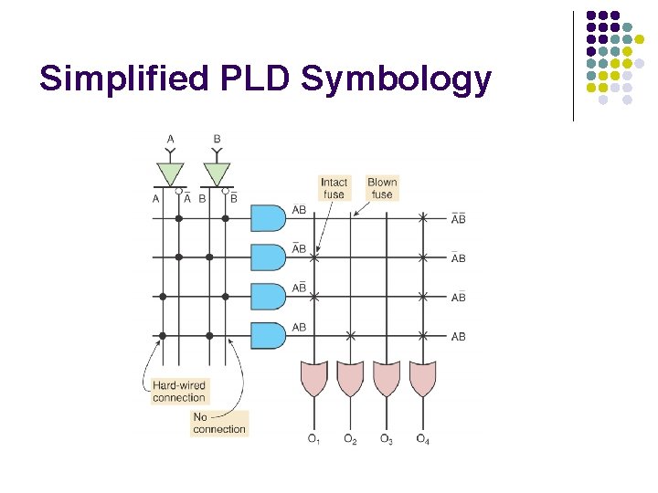
Simplified PLD Symbology
PLD Architectures l l Different architectural designs of the inner circuitry of PLDs. PROM: programmable ROM PAL: programmable array logic FPLA: field programmable logic array
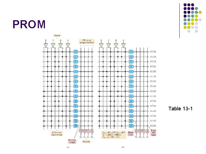
PROM Table 13 -1
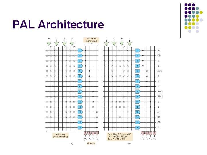
PAL Architecture
FPLA l Used a programmable AND array as well as a programmable OR array.
- Slides: 18