Programmable Data Communication Blocks Alex Doboli Ph D

Programmable Data Communication Blocks Alex Doboli, Ph. D. Department of Electrical and Computer Engineering State University of New York at Stony Brook Email: adoboli@ece. sunysb. edu ©Alex Doboli 2006
Overview of the Chapter • Design methods for optimizing the communications subsystems • SPI and UART modules (Hardware & software) • Communication subsystems are a main component of a system • Influence system speed and power consumption • API routines: channel configuration & management, data sent/receive • Design methodology for optimized implementation – Required primitives, available hardware, performance – Selecting the modules, sharing, module implementation ©Alex Doboli 2006
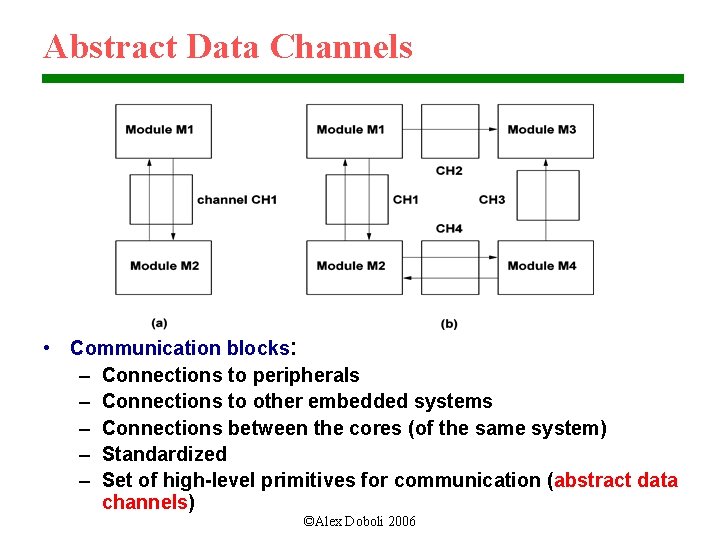
Abstract Data Channels • Communication blocks: – Connections to peripherals – Connections to other embedded systems – Connections between the cores (of the same system) – Standardized – Set of high-level primitives for communication (abstract data channels) ©Alex Doboli 2006
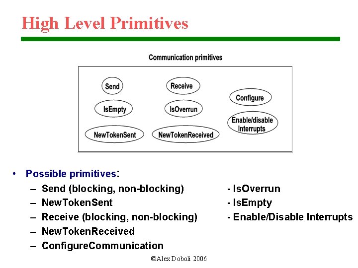
High Level Primitives • Possible primitives: – Send (blocking, non-blocking) – New. Token. Sent – Receive (blocking, non-blocking) – New. Token. Received – Configure. Communication ©Alex Doboli 2006 - Is. Overrun - Is. Empty - Enable/Disable Interrupts
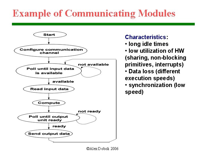
Example of Communicating Modules Characteristics: • long idle times • low utilization of HW (sharing, non-blocking primitives, interrupts) • Data loss (different execution speeds) • synchronization (low speed) ©Alex Doboli 2006
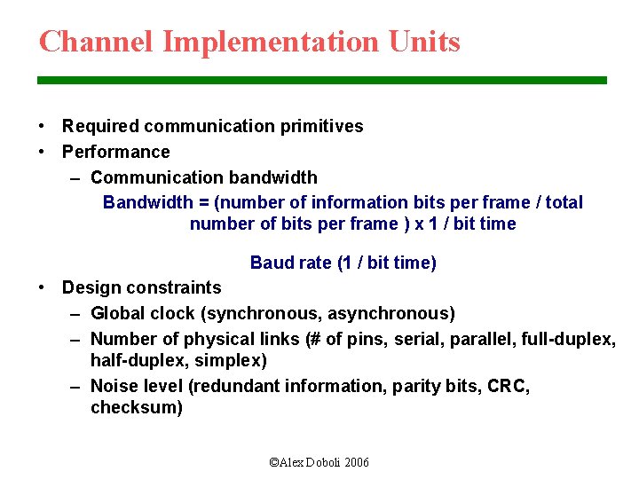
Channel Implementation Units • Required communication primitives • Performance – Communication bandwidth Bandwidth = (number of information bits per frame / total number of bits per frame ) x 1 / bit time Baud rate (1 / bit time) • Design constraints – Global clock (synchronous, asynchronous) – Number of physical links (# of pins, serial, parallel, full-duplex, half-duplex, simplex) – Noise level (redundant information, parity bits, CRC, checksum) ©Alex Doboli 2006
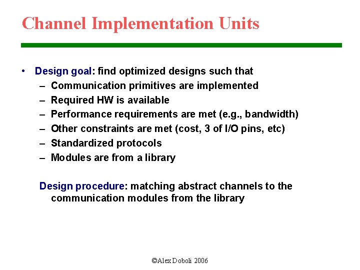
Channel Implementation Units • Design goal: find optimized designs such that – Communication primitives are implemented – Required HW is available – Performance requirements are met (e. g. , bandwidth) – Other constraints are met (cost, 3 of I/O pins, etc) – Standardized protocols – Modules are from a library Design procedure: matching abstract channels to the communication modules from the library ©Alex Doboli 2006
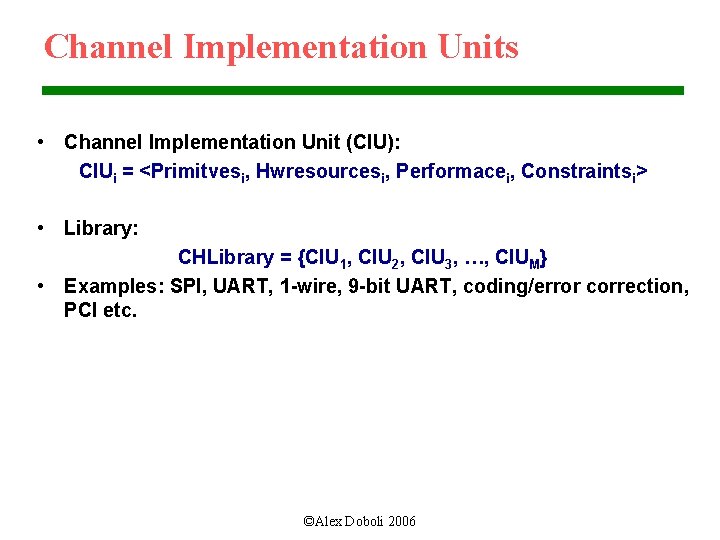
Channel Implementation Units • Channel Implementation Unit (CIU): CIUi = <Primitvesi, Hwresourcesi, Performacei, Constraintsi> • Library: CHLibrary = {CIU 1, CIU 2, CIU 3, …, CIUM} • Examples: SPI, UART, 1 -wire, 9 -bit UART, coding/error correction, PCI etc. ©Alex Doboli 2006
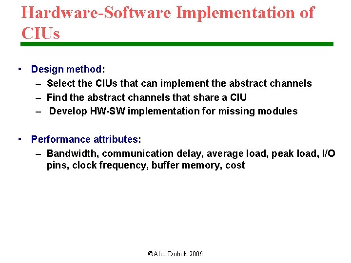
Hardware-Software Implementation of CIUs • Design method: – Select the CIUs that can implement the abstract channels – Find the abstract channels that share a CIU – Develop HW-SW implementation for missing modules • Performance attributes: – Bandwidth, communication delay, average load, peak load, I/O pins, clock frequency, buffer memory, cost ©Alex Doboli 2006
Hardware-Software Implementation of CIUs • CIU allocation: – For each abstract channel, identify the library modules that can be used in implementation – Look at primitives, performance, needed HW, constraints • Abstract channel mapping: – Find abstract channels that can share a CIU (reduces cost) – Scheduling (arbitration) – Buffer insertion – Glue and control logic for sharing • Developing (missing) CIUs: – Missing primitives – Performance requirements are not met by available modules ©Alex Doboli 2006
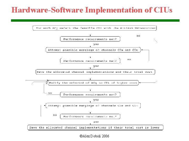
Hardware-Software Implementation of CIUs ©Alex Doboli 2006
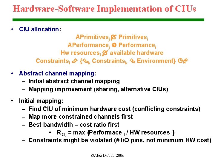
Hardware-Software Implementation of CIUs • CIU allocation: APrimitivesj Primitivesi APerformancej Performancei Hw resourcesi available hardware Constraintsi { k Constraintsk Environment} • Abstract channel mapping: – Initial abstract channel mapping – Mapping improvement (sharing, alternative CIUs) • Initial mapping: – Find CIU of minimum hardware cost (conflicting constraints) – Map more constrained channels first – Best bandwidth – cost ratio first • RCIj = max {Performace I / HW resources i} – Constraints might be violated (# I/O pins, not minimum HW cost) ©Alex Doboli 2006
Hardware-Software Implementation of CIUs • Mapping improvement: – Merge two channels CIm and Cin • Primitives can be delivered by a single module • “Cumulated” performance can be met by the single module • Scheduling policy: round-robin, highest priority channel first – If performance not met, switch to a CIU with higher performance ©Alex Doboli 2006
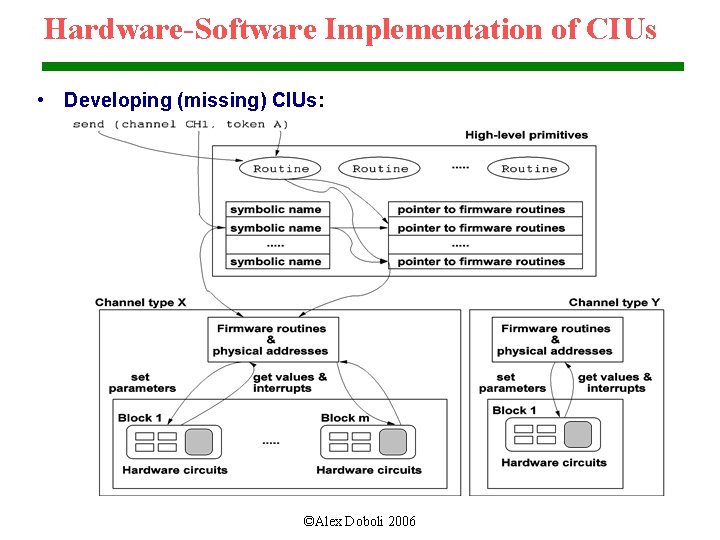
Hardware-Software Implementation of CIUs • Developing (missing) CIUs: ©Alex Doboli 2006
Serial Peripheral Interface (SPI) • Characteristics: – Full-duplex, synchronous, serial transmission – SPI master (SPIM), SPI slave (SPIS) • Communication: – SPIM sends bits serially to SPIS – Simultaneously, SPIS sends bits serially to SPIM – SPIM generates clock signal (SCLK) for SPIS – SPIM generates select signal (SS) for SPIS ©Alex Doboli 2006
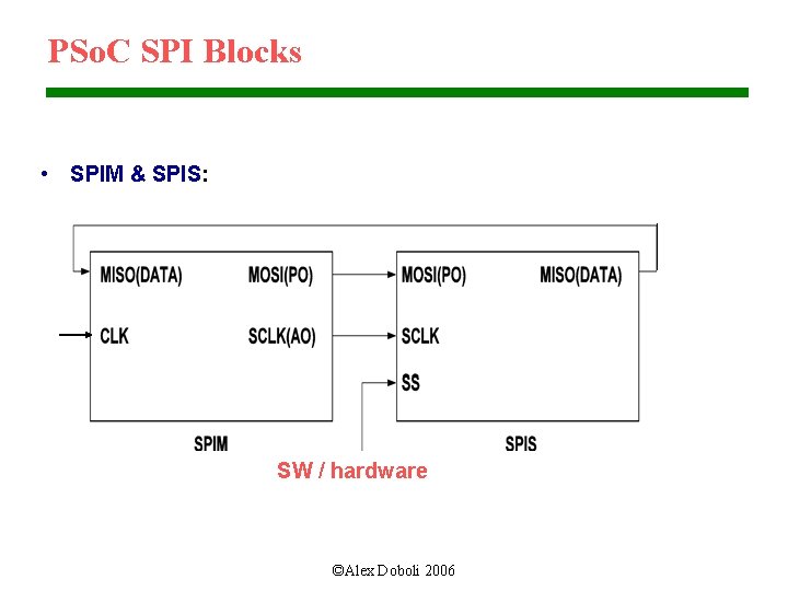
PSo. C SPI Blocks • SPIM & SPIS: SW / hardware ©Alex Doboli 2006
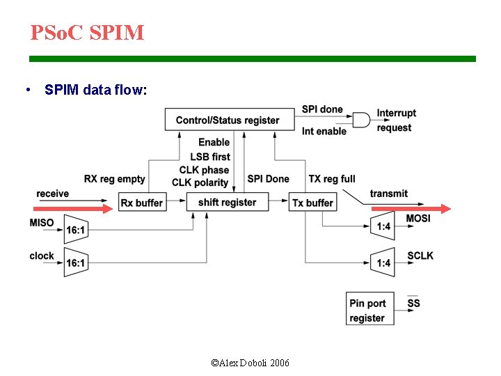
PSo. C SPIM • SPIM data flow: ©Alex Doboli 2006
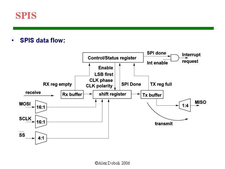
SPIS • SPIS data flow: ©Alex Doboli 2006
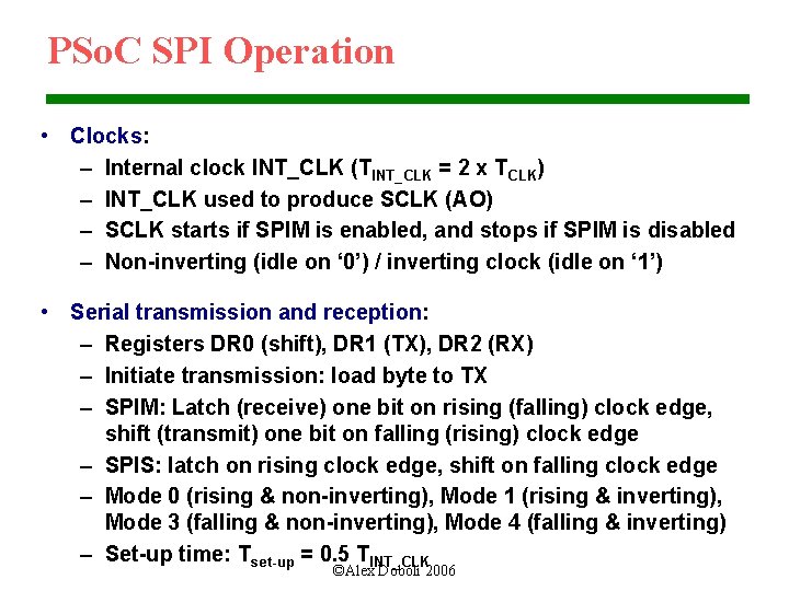
PSo. C SPI Operation • Clocks: – Internal clock INT_CLK (TINT_CLK = 2 x TCLK) – INT_CLK used to produce SCLK (AO) – SCLK starts if SPIM is enabled, and stops if SPIM is disabled – Non-inverting (idle on ‘ 0’) / inverting clock (idle on ‘ 1’) • Serial transmission and reception: – Registers DR 0 (shift), DR 1 (TX), DR 2 (RX) – Initiate transmission: load byte to TX – SPIM: Latch (receive) one bit on rising (falling) clock edge, shift (transmit) one bit on falling (rising) clock edge – SPIS: latch on rising clock edge, shift on falling clock edge – Mode 0 (rising & non-inverting), Mode 1 (rising & inverting), Mode 3 (falling & non-inverting), Mode 4 (falling & inverting) – Set-up time: Tset-up = 0. 5 TINT_CLK ©Alex Doboli 2006
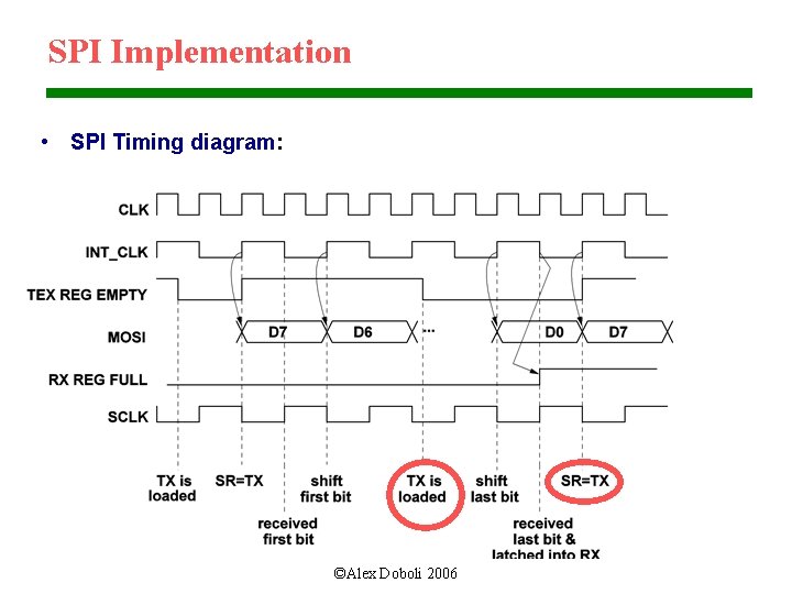
SPI Implementation • SPI Timing diagram: ©Alex Doboli 2006
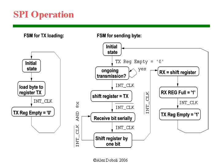
SPI Operation ©Alex Doboli 2006
PSo. C SPI Programming • Register FN: – Bits 2 -0: “ 110” -> SPI (both SPIM and SPIS) – Bit 3: “ 0” -> SPIM, “ 1” -> SPIS – Bit 4: “ 0” -> interrupt on TX Reg Empty (new byte can be loaded to TX), “ 1” -> SPI Complete (new byte received) ©Alex Doboli 2006
PSo. C SPI Programming • Register CR 0: – Bit 0: Enable/Disable – Bit 1: “ 0” -> non-inverting clock, “ 1” -> inverting clock – Bit 2: ‘ 0’ -> latching on rising clock, ‘ 1’ -> latching on falling clock – Bit 3: RX_Reg_Full (‘ 0’ -> RX empty, ‘ 1’ -> RX full) – Bit 4: TX_Reg_Empty (‘ 0’ -> TX has 1 byte, ‘ 1’ -> TX empty) – Bit 5: SPI Complete (‘ 1’ -> byte was shifted out, ‘ 0’ -> otherwise) – Bit 6: RX Overrun (‘ 0’ -> no overrun, ‘ 1’ overrun) – Bt 7: ‘ 0’ -> MSB first, ‘ 1’ -> LSB first ©Alex Doboli 2006
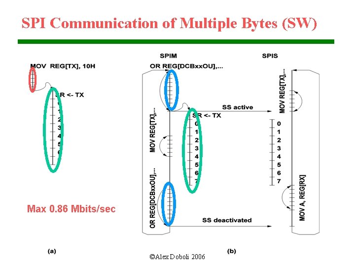
SPI Communication of Multiple Bytes (SW) Max 0. 86 Mbits/sec ©Alex Doboli 2006
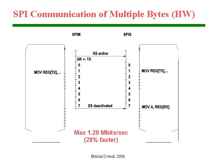
SPI Communication of Multiple Bytes (HW) Max 1. 20 Mbits/sec (28% faster) ©Alex Doboli 2006
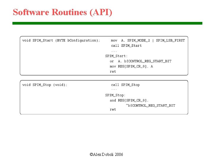
Software Routines (API) ©Alex Doboli 2006
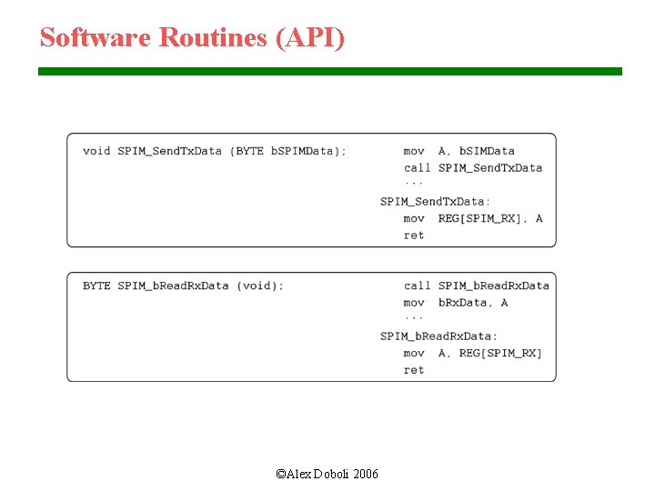
Software Routines (API) ©Alex Doboli 2006
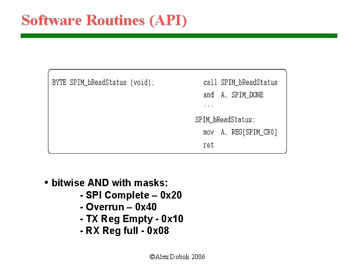
Software Routines (API) • bitwise AND with masks: - SPI Complete – 0 x 20 - Overrun – 0 x 40 - TX Reg Empty - 0 x 10 - RX Reg full - 0 x 08 ©Alex Doboli 2006
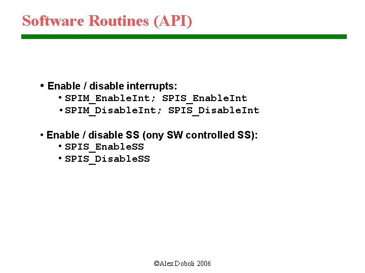
Software Routines (API) • Enable / disable interrupts: • SPIM_Enable. Int; SPIS_Enable. Int • SPIM_Disable. Int; SPIS_Disable. Int • Enable / disable SS (ony SW controlled SS): • SPIS_Enable. SS • SPIS_Disable. SS ©Alex Doboli 2006
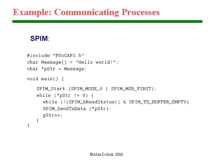
Example: Communicating Processes SPIM: ©Alex Doboli 2006
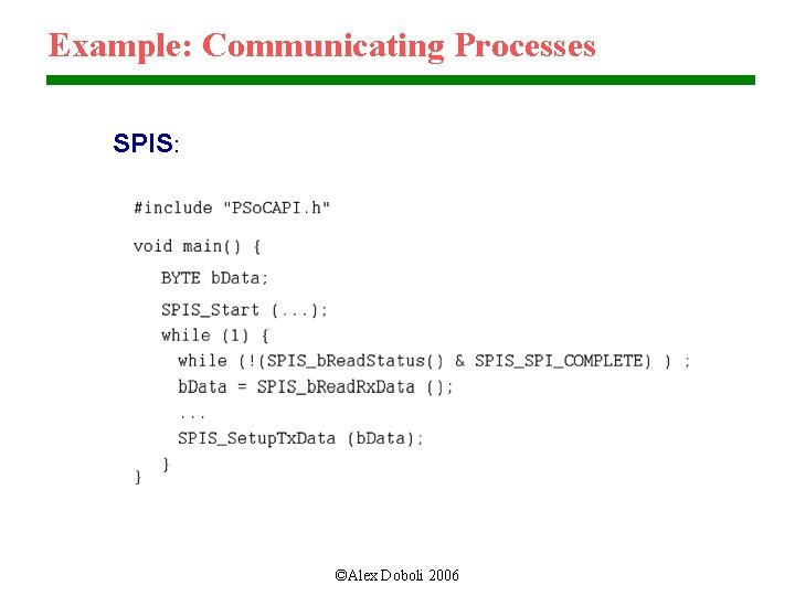
Example: Communicating Processes SPIS: ©Alex Doboli 2006
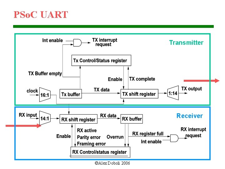
Universal Asynchronous Receiver Transmitter (UART) • Characteristics: – 8 bit, duplex, serial communication • Communication: – Two independent blocks: transmitter and receiver – Implemented using 2 programmable PSo. C blocks ©Alex Doboli 2006
PSo. C UART Transmitter Receiver ©Alex Doboli 2006
PSo. C UART Transmit Operation • Clocks: – Internal clock INT_CLK (TINT_CLK = 8 x TCLK) • Serial transmission: – Registers DR 0 (shift), DR 1 (TX), DR 2 (RX), CR 0 (control) – Output = ‘ 1’, if no data in TX or block not enabled – Transmit: data is loaded into TX, data loaded into the shift register, bits shifted out at each clock cycle – Transmitted frame: bit start, 8 bits, parity bit, bit stop ©Alex Doboli 2006
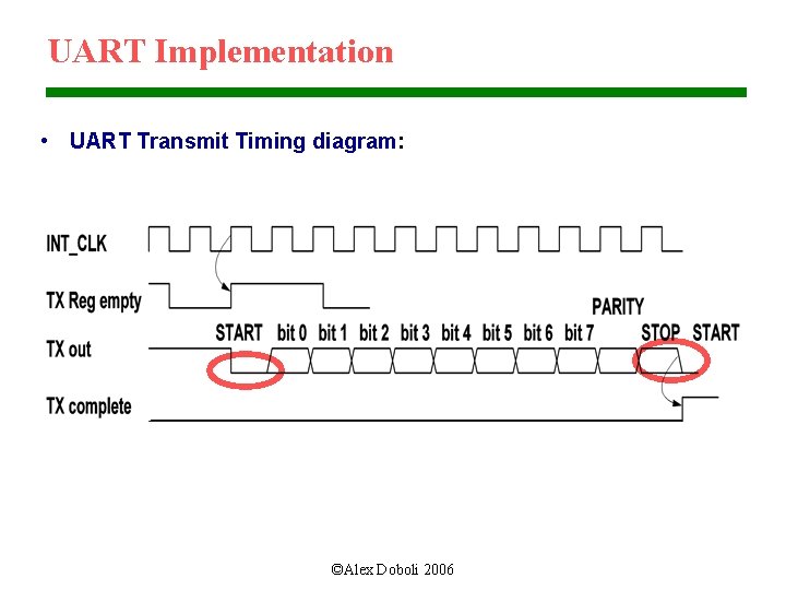
UART Implementation • UART Transmit Timing diagram: ©Alex Doboli 2006
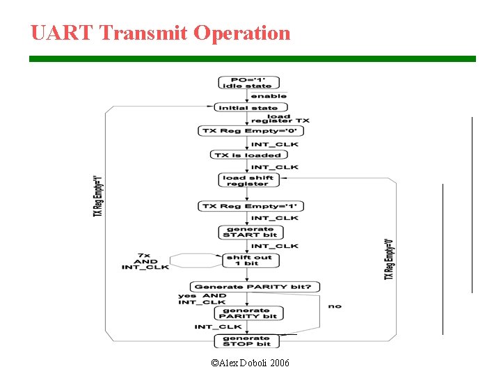
UART Transmit Operation ©Alex Doboli 2006
PSo. C UART Receive Operation • Serial reception: – Registers DR 0 (shift), DR 1 (TX), DR 2 (RX), CR 0 (control) – Initiated by START bit (‘ 0’) – One bit received at the rate equal to the set baud rate – Finished after receiving STOP bit (‘ 1’): sets flag, data available in RX, back to the reception state – Flags: RX Active (ongoing reception), RX Reg full (new byte received), Framing error, Parity error, Overrun ©Alex Doboli 2006
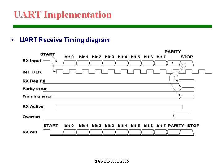
UART Implementation • UART Receive Timing diagram: ©Alex Doboli 2006
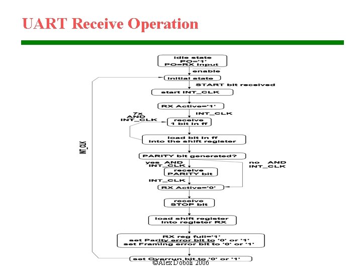
UART Receive Operation ©Alex Doboli 2006
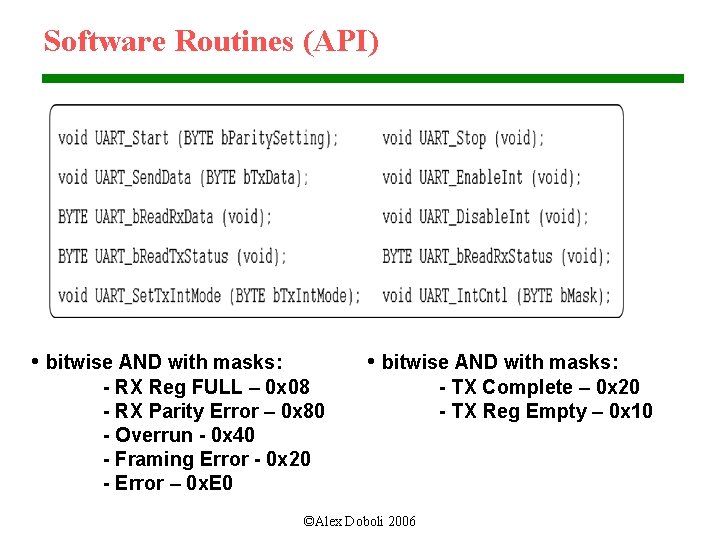
Software Routines (API) • bitwise AND with masks: - RX Reg FULL – 0 x 08 - RX Parity Error – 0 x 80 - Overrun - 0 x 40 - Framing Error - 0 x 20 - Error – 0 x. E 0 ©Alex Doboli 2006 - TX Complete – 0 x 20 - TX Reg Empty – 0 x 10
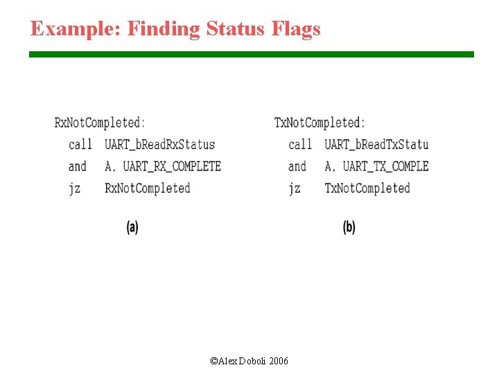
Example: Finding Status Flags ©Alex Doboli 2006
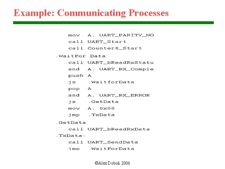
Example: Communicating Processes ©Alex Doboli 2006
- Slides: 42