ProcessVariationResistant Dynamic Power Optimization for VLSI Circuits Fei

![Input-specific optimization Dominating path Can be [1, 41] 41 1 1 Why need a Input-specific optimization Dominating path Can be [1, 41] 41 1 1 Why need a](https://slidetodoc.com/presentation_image_h2/0f3e163a2add73e1391b049178173785/image-32.jpg)

- Slides: 48

Process-Variation-Resistant Dynamic Power Optimization for VLSI Circuits Fei Hu Department of ECE Auburn University, AL 36849 Ph. D. Dissertation Committee: Dr. Vishwani D. Agrawal Dr. Foster Dai Dr. Darrel Hankerson Dr. Saad Biaz (Outside Reader) November 16, 2005

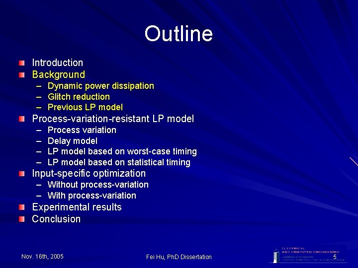
Outline Introduction Background – – – Dynamic power dissipation Glitch reduction Previous LP model Process-variation-resistant LP model – – Process variation Delay model LP model based on worst-case timing LP model based on statistical timing Input-specific optimization – Without process-variation – With process-variation Experimental results Conclusion Nov. 16 th, 2005 Fei Hu, Ph. D Dissertation 2

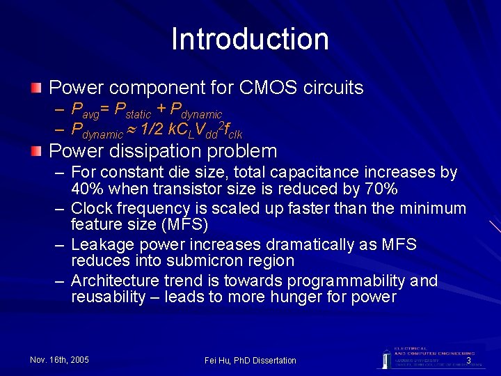
Introduction Power component for CMOS circuits – Pavg= Pstatic + Pdynamic – Pdynamic 1/2 k. CLVdd 2 fclk Power dissipation problem – For constant die size, total capacitance increases by 40% when transistor size is reduced by 70% – Clock frequency is scaled up faster than the minimum feature size (MFS) – Leakage power increases dramatically as MFS reduces into submicron region – Architecture trend is towards programmability and reusability – leads to more hunger for power Nov. 16 th, 2005 Fei Hu, Ph. D Dissertation 3

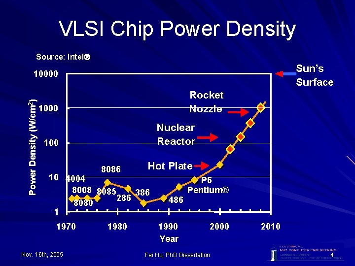
VLSI Chip Power Density Source: Intel Sun’s Surface Power Density (W/cm 2) 10000 Rocket Nozzle 1000 Nuclear Reactor 100 8086 Hot Plate 10 4004 8008 8085 386 286 8080 1 1970 Nov. 16 th, 2005 1980 P 6 Pentium® 486 1990 Year 2000 Fei Hu, Ph. D Dissertation 2010 4

Outline Introduction Background – Dynamic power dissipation – Glitch reduction – Previous LP model Process-variation-resistant LP model – – Process variation Delay model LP model based on worst-case timing LP model based on statistical timing Input-specific optimization – Without process-variation – With process-variation Experimental results Conclusion Nov. 16 th, 2005 Fei Hu, Ph. D Dissertation 5

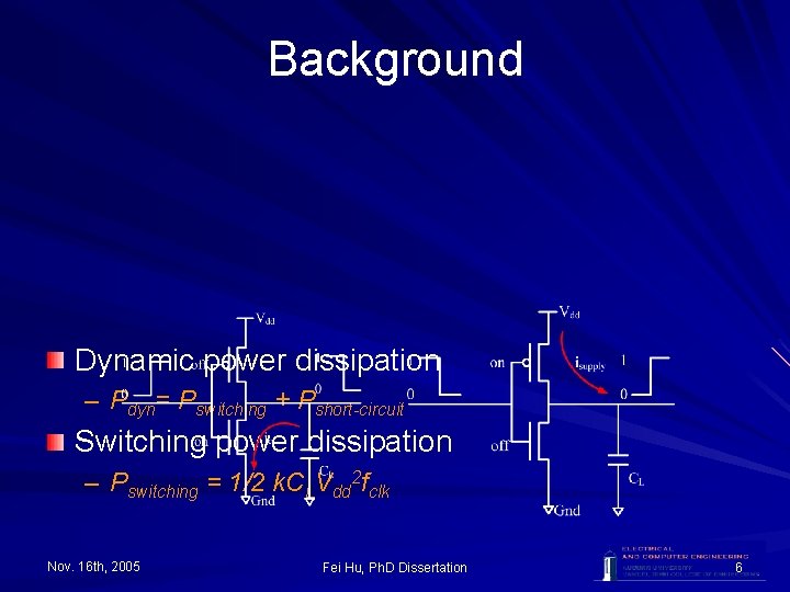
Background Dynamic power dissipation – Pdyn= Pswitching + Pshort-circuit Switching power dissipation – Pswitching = 1/2 k. CLVdd 2 fclk Nov. 16 th, 2005 Fei Hu, Ph. D Dissertation 6

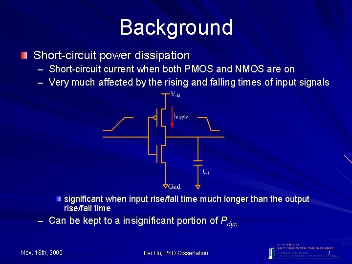
Background Short-circuit power dissipation – Short-circuit current when both PMOS and NMOS are on – Very much affected by the rising and falling times of input signals significant when input rise/fall time much longer than the output rise/fall time – Can be kept to a insignificant portion of Pdyn Nov. 16 th, 2005 Fei Hu, Ph. D Dissertation 7

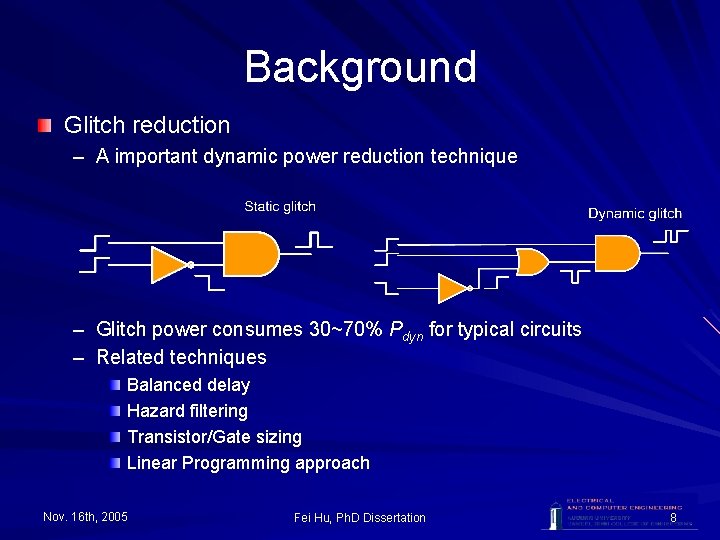
Background Glitch reduction – A important dynamic power reduction technique – Glitch power consumes 30~70% Pdyn for typical circuits – Related techniques Balanced delay Hazard filtering Transistor/Gate sizing Linear Programming approach Nov. 16 th, 2005 Fei Hu, Ph. D Dissertation 8

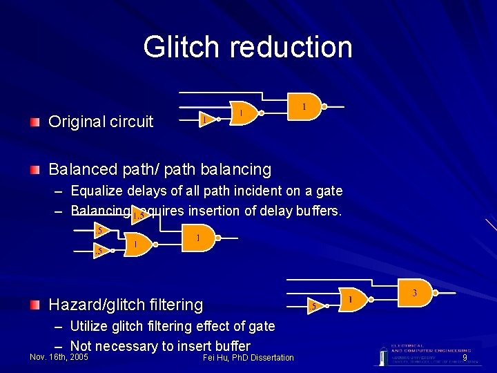
Glitch reduction Original circuit Balanced path/ path balancing – Equalize delays of all path incident on a gate – Balancing requires insertion of delay buffers. Hazard/glitch filtering – Utilize glitch filtering effect of gate – Not necessary to insert buffer Nov. 16 th, 2005 Fei Hu, Ph. D Dissertation 9

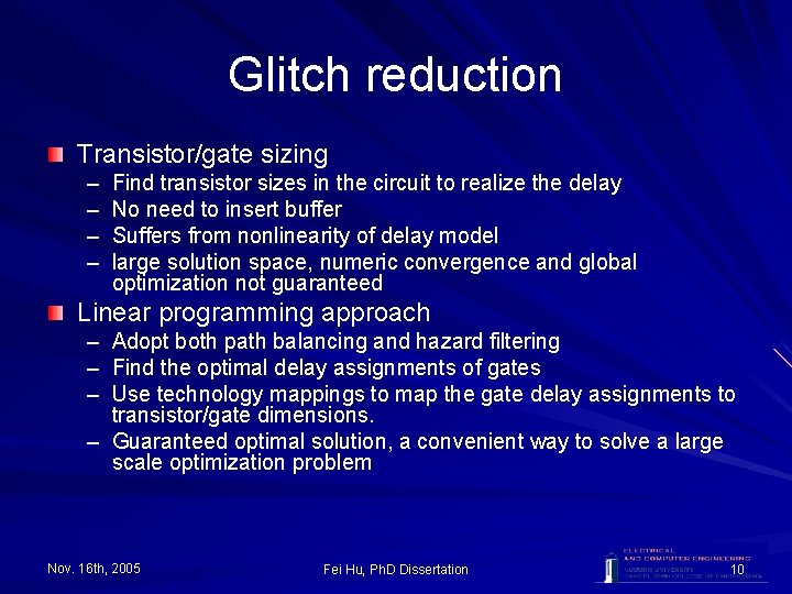
Glitch reduction Transistor/gate sizing – – Find transistor sizes in the circuit to realize the delay No need to insert buffer Suffers from nonlinearity of delay model large solution space, numeric convergence and global optimization not guaranteed Linear programming approach – Adopt both path balancing and hazard filtering – Find the optimal delay assignments of gates – Use technology mappings to map the gate delay assignments to transistor/gate dimensions. – Guaranteed optimal solution, a convenient way to solve a large scale optimization problem Nov. 16 th, 2005 Fei Hu, Ph. D Dissertation 10

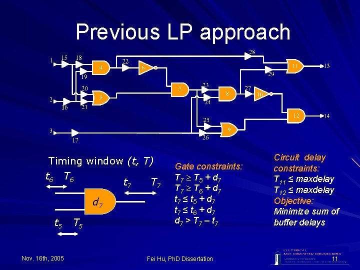
Previous LP approach Timing window (t, T) t 6 T 6 t 7 T 7 d 7 t 5 Nov. 16 th, 2005 T 5 Gate constraints: T 7 T 5 + d 7 T 7 T 6 + d 7 t 7 ≤ t 5 + d 7 t 7 ≤ t 6 + d 7 > T 7 – t 7 Fei Hu, Ph. D Dissertation Circuit delay constraints: T 11 ≤ maxdelay T 12 ≤ maxdelay Objective: Minimize sum of buffer delays 11

Outline Introduction Background – Dynamic power dissipation – Glitch reduction – Previous LP model Process-variation-resistant LP model – – Process variation Delay model LP model based on worst-case timing LP model based on statistical timing Input-specific optimization – Without process-variation – With process-variation Experimental results Conclusion Nov. 16 th, 2005 Fei Hu, Ph. D Dissertation 12

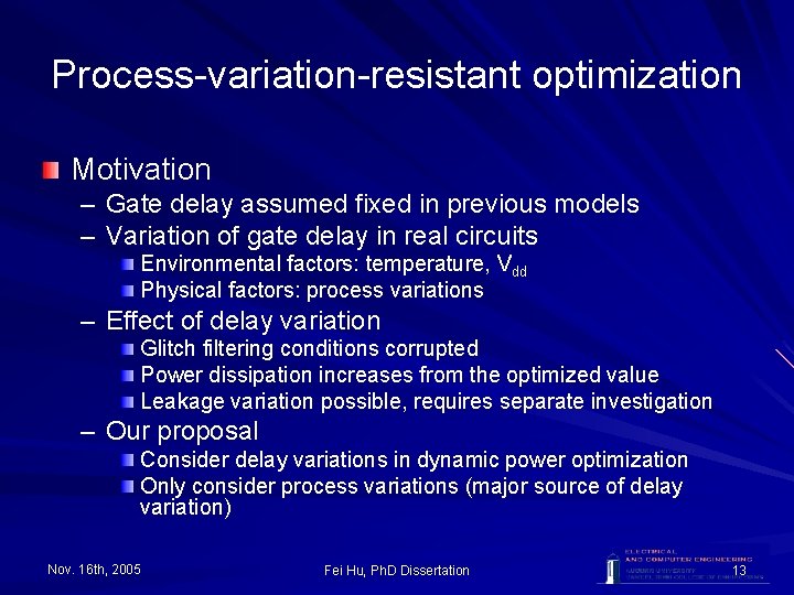
Process-variation-resistant optimization Motivation – Gate delay assumed fixed in previous models – Variation of gate delay in real circuits Environmental factors: temperature, Vdd Physical factors: process variations – Effect of delay variation Glitch filtering conditions corrupted Power dissipation increases from the optimized value Leakage variation possible, requires separate investigation – Our proposal Consider delay variations in dynamic power optimization Only consider process variations (major source of delay variation) Nov. 16 th, 2005 Fei Hu, Ph. D Dissertation 13

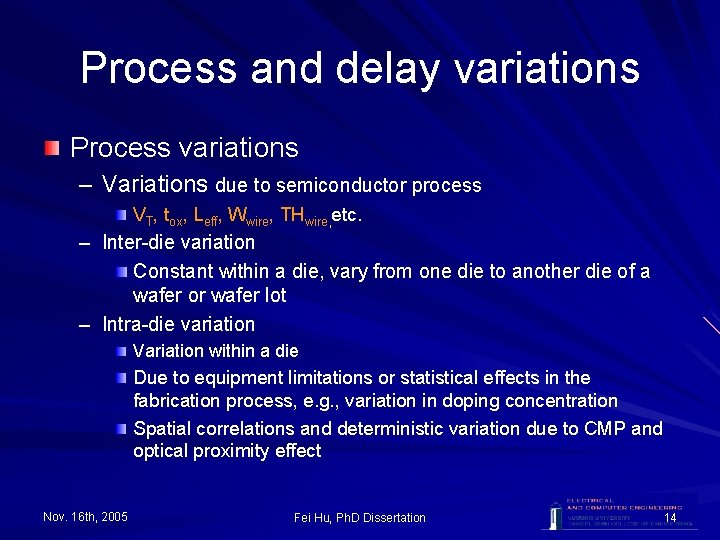
Process and delay variations Process variations – Variations due to semiconductor process VT, tox, Leff, Wwire, THwire, etc. – Inter-die variation Constant within a die, vary from one die to another die of a wafer or wafer lot – Intra-die variation Variation within a die Due to equipment limitations or statistical effects in the fabrication process, e. g. , variation in doping concentration Spatial correlations and deterministic variation due to CMP and optical proximity effect Nov. 16 th, 2005 Fei Hu, Ph. D Dissertation 14

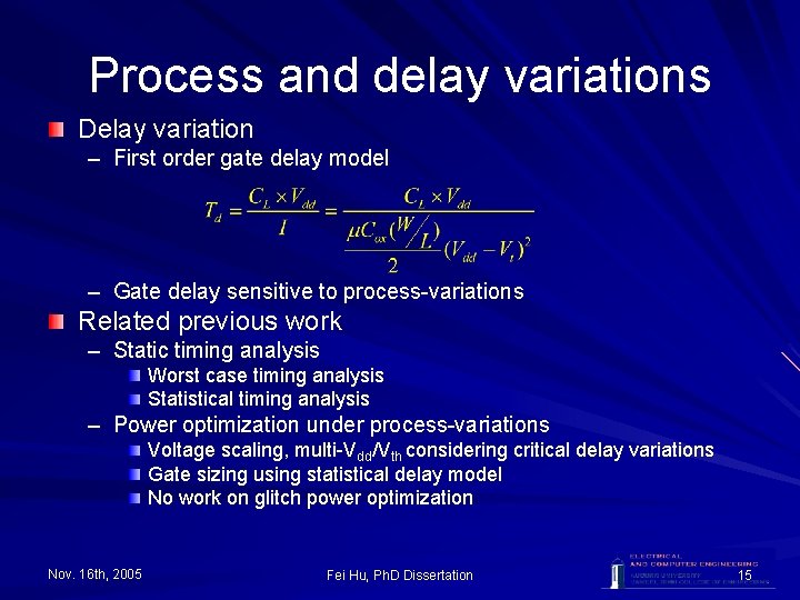
Process and delay variations Delay variation – First order gate delay model – Gate delay sensitive to process-variations Related previous work – Static timing analysis Worst case timing analysis Statistical timing analysis – Power optimization under process-variations Voltage scaling, multi-Vdd/Vth considering critical delay variations Gate sizing using statistical delay model No work on glitch power optimization Nov. 16 th, 2005 Fei Hu, Ph. D Dissertation 15

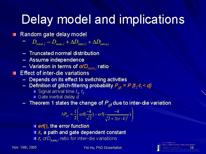
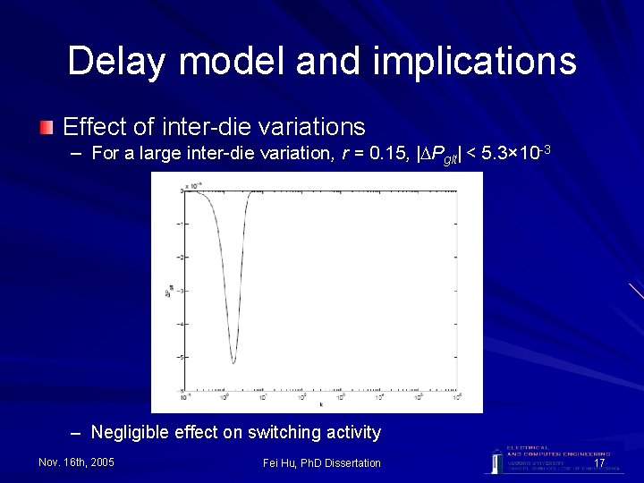
Delay model and implications Random gate delay model – – Truncated normal distribution – Assume independence – Variation in terms of σ/Dnom, i ratio Effect of inter-die variations – Depends on its effect to switching activities – Definition of glitch-filtering probability Pglt = P {t 2 -t 1< d} Signal arrival time t 1, t 2 Gate inertial delay d – Theorem 1 states the change of Pglt due to inter-die variation erf(), the error function k, a path and gate dependent constant r, σ/Dnom, i ratio for inter-die variations Nov. 16 th, 2005 Fei Hu, Ph. D Dissertation 16

Delay model and implications Effect of inter-die variations – For a large inter-die variation, r = 0. 15, | Pglt| < 5. 3× 10 -3 – Negligible effect on switching activity Nov. 16 th, 2005 Fei Hu, Ph. D Dissertation 17

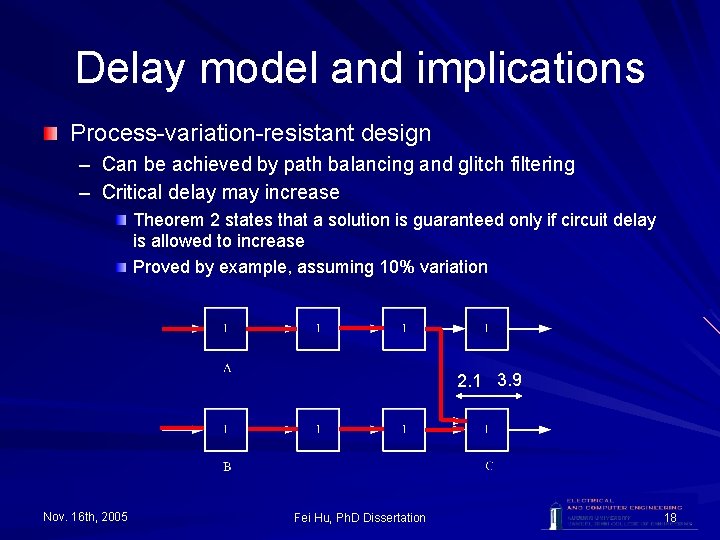
Delay model and implications Process-variation-resistant design – Can be achieved by path balancing and glitch filtering – Critical delay may increase Theorem 2 states that a solution is guaranteed only if circuit delay is allowed to increase Proved by example, assuming 10% variation 2. 1 3. 9 Nov. 16 th, 2005 Fei Hu, Ph. D Dissertation 18

LP model based on worst-case timing Timing model Nov. 16 th, 2005 Fei Hu, Ph. D Dissertation 19

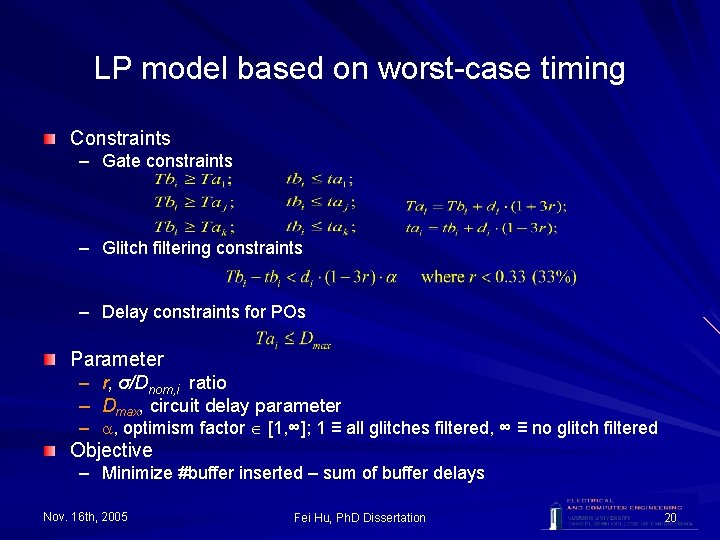
LP model based on worst-case timing Constraints – Gate constraints – Glitch filtering constraints – Delay constraints for POs Parameter – r, σ/Dnom, i ratio – Dmax, circuit delay parameter – , optimism factor [1, ∞]; 1 ≡ all glitches filtered, ∞ ≡ no glitch filtered Objective – Minimize #buffer inserted – sum of buffer delays Nov. 16 th, 2005 Fei Hu, Ph. D Dissertation 20

LP model based on statistical timing Worst-case timing tends to be too pessimistic Statistical timing model with random variables Nov. 16 th, 2005 Fei Hu, Ph. D Dissertation 21

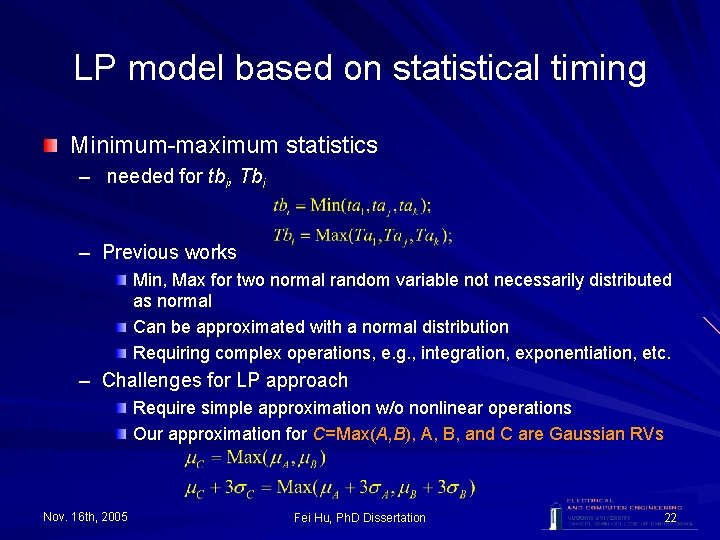
LP model based on statistical timing Minimum-maximum statistics – needed for tbi, Tbi – Previous works Min, Max for two normal random variable not necessarily distributed as normal Can be approximated with a normal distribution Requiring complex operations, e. g. , integration, exponentiation, etc. – Challenges for LP approach Require simple approximation w/o nonlinear operations Our approximation for C=Max(A, B), A, B, and C are Gaussian RVs Nov. 16 th, 2005 Fei Hu, Ph. D Dissertation 22

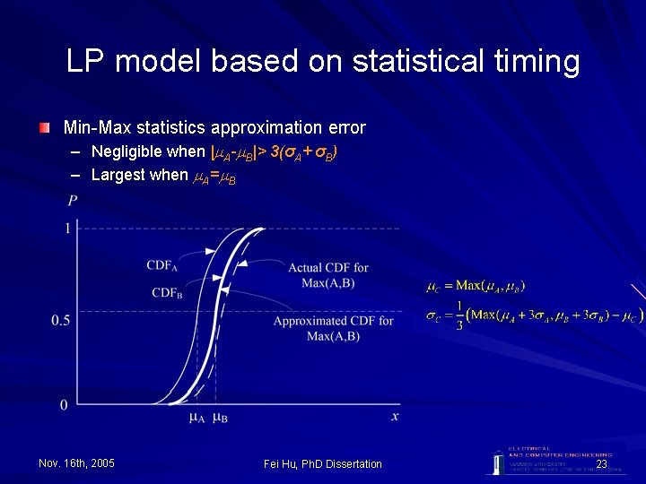
LP model based on statistical timing Min-Max statistics approximation error – Negligible when | A- B|> 3(σA+ σB) – Largest when A= B Nov. 16 th, 2005 Fei Hu, Ph. D Dissertation 23

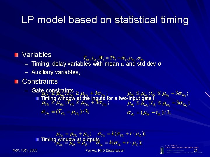
LP model based on statistical timing Variables – Timing, delay variables with mean and std dev σ – Auxiliary variables, Constraints – Gate constraints Timing window at the inputs for a two-input gate i Timing window at outputs Nov. 16 th, 2005 Fei Hu, Ph. D Dissertation 24

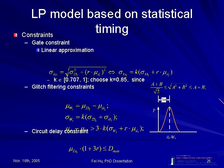
LP model based on statistical timing Constraints – Gate constraint Linear approximation – k [0. 707, 1]; choose k=0. 85, since – Glitch filtering constraints – Circuit delay constraint Nov. 16 th, 2005 Fei Hu, Ph. D Dissertation 25

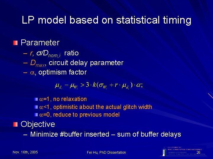
LP model based on statistical timing Parameter – r, σ/Dnom, i ratio – Dmax, circuit delay parameter – , optimism factor =1, no relaxation <1, optimistic about the actual glitch width =0, reduce to previous model Objective – Minimize #buffer inserted – sum of buffer delays Nov. 16 th, 2005 Fei Hu, Ph. D Dissertation 26

Outline Introduction Background – Dynamic power dissipation – Glitch reduction – Previous LP model Process-variation-resistant LP model – – Process variation Delay model LP model based on worst-case timing LP model based on statistical timing Input-specific optimization – Without process-variation – With process-variation Experimental results Conclusion Nov. 16 th, 2005 Fei Hu, Ph. D Dissertation 27

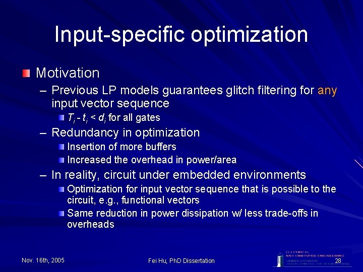
Input-specific optimization Motivation – Previous LP models guarantees glitch filtering for any input vector sequence Ti - ti < di for all gates – Redundancy in optimization Insertion of more buffers Increased the overhead in power/area – In reality, circuit under embedded environments Optimization for input vector sequence that is possible to the circuit, e. g. , functional vectors Same reduction in power dissipation w/ less trade-offs in overheads Nov. 16 th, 2005 Fei Hu, Ph. D Dissertation 28

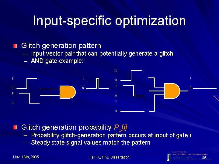
Input-specific optimization Glitch generation pattern – Input vector pair that can potentially generate a glitch – AND gate example: Glitch generation probability Pg[i] – – Probability glitch-generation pattern occurs at input of gate i Steady state signal values match the pattern Nov. 16 th, 2005 Fei Hu, Ph. D Dissertation 29

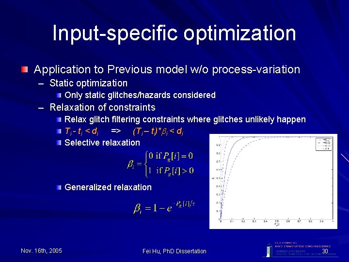
Input-specific optimization Application to Previous model w/o process-variation – Static optimization Only static glitches/hazards considered – Relaxation of constraints Relax glitch filtering constraints where glitches unlikely happen Ti - ti < di => (Ti – ti)* i < di Selective relaxation Generalized relaxation Nov. 16 th, 2005 Fei Hu, Ph. D Dissertation 30

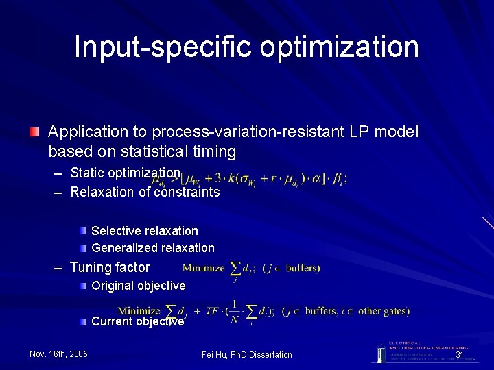
Input-specific optimization Application to process-variation-resistant LP model based on statistical timing – Static optimization – Relaxation of constraints Selective relaxation Generalized relaxation – Tuning factor Original objective Current objective Nov. 16 th, 2005 Fei Hu, Ph. D Dissertation 31
![Inputspecific optimization Dominating path Can be 1 41 41 1 1 Why need a Input-specific optimization Dominating path Can be [1, 41] 41 1 1 Why need a](https://slidetodoc.com/presentation_image_h2/0f3e163a2add73e1391b049178173785/image-32.jpg)
Input-specific optimization Dominating path Can be [1, 41] 41 1 1 Why need a tuning factor 0 0 1 1 – Dominating path affected critical delay distribution Nov. 16 th, 2005 Fei Hu, Ph. D Dissertation 32

Outline Introduction Background – Dynamic power dissipation – Glitch reduction – Previous LP model Process-variation-resistant LP model – – Process variation Delay model LP model based on worst-case timing LP model based on statistical timing Input-specific optimization – Without process-variation – With process-variation Experimental results Conclusion Nov. 16 th, 2005 Fei Hu, Ph. D Dissertation 33

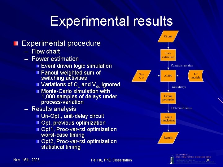
Experimental results Experimental procedure – Flow chart – Power estimation Event driven logic simulation Fanout weighted sum of switching activities Variations of CL and Vdd ignored Monte-Carlo simulation with 1, 000 samples of delays under process-variation – Results analysis Un-Opt. , unit-delay circuit Opt, previous optimization Opt 1, Proc-var-rst optimization worst-case timing Opt 2, Proc-var-rst optimization statistical timing Nov. 16 th, 2005 Fei Hu, Ph. D Dissertation 34

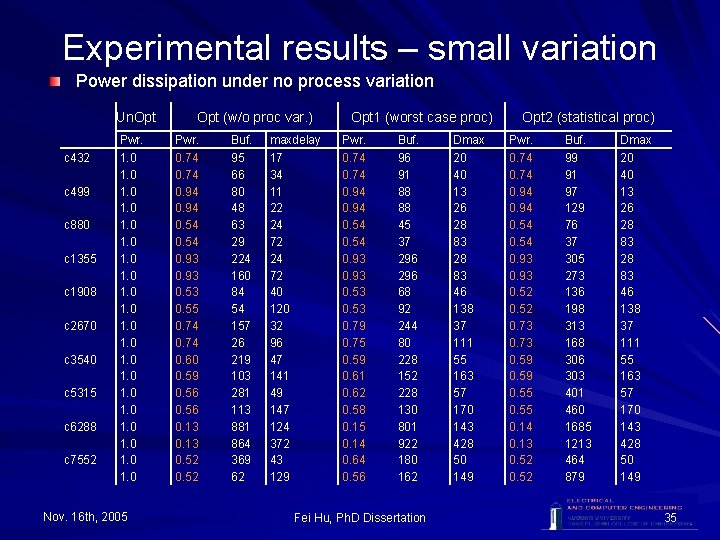
Experimental results – small variation Power dissipation under no process variation Un. Opt c 432 c 499 c 880 c 1355 c 1908 c 2670 c 3540 c 5315 c 6288 c 7552 Pwr. 1. 0 1. 0 Nov. 16 th, 2005 Opt (w/o proc var. ) Pwr. 0. 74 0. 94 0. 54 0. 93 0. 53 0. 55 0. 74 0. 60 0. 59 0. 56 0. 13 0. 52 Buf. 95 66 80 48 63 29 224 160 84 54 157 26 219 103 281 113 881 864 369 62 maxdelay 17 34 11 22 24 72 40 120 32 96 47 141 49 147 124 372 43 129 Opt 1 (worst case proc) Pwr. 0. 74 0. 94 0. 54 0. 93 0. 53 0. 79 0. 75 0. 59 0. 61 0. 62 0. 58 0. 15 0. 14 0. 64 0. 56 Buf. 96 91 88 88 45 37 296 68 92 244 80 228 152 228 130 801 922 180 162 Fei Hu, Ph. D Dissertation Dmax 20 40 13 26 28 83 46 138 37 111 55 163 57 170 143 428 50 149 Opt 2 (statistical proc) Pwr. 0. 74 0. 94 0. 54 0. 93 0. 52 0. 73 0. 59 0. 55 0. 14 0. 13 0. 52 Buf. 99 91 97 129 76 37 305 273 136 198 313 168 306 303 401 460 1685 1213 464 879 Dmax 20 40 13 26 28 83 46 138 37 111 55 163 57 170 143 428 50 149 35

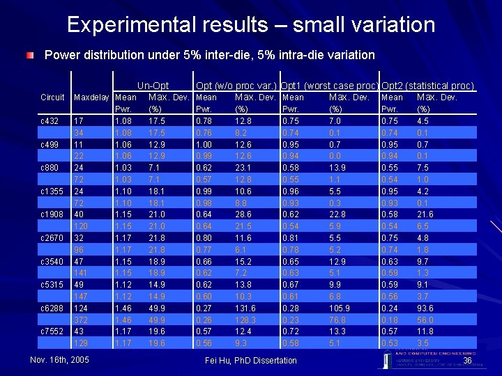
Experimental results – small variation Power distribution under 5% inter-die, 5% intra-die variation Circuit c 432 c 499 c 880 c 1355 c 1908 c 2670 c 3540 c 5315 c 6288 c 7552 Un-Opt (w/o proc var. ) Opt 1 (worst case proc) Opt 2 (statistical proc) Maxdelay Mean Max. Dev. 17 34 11 22 24 72 40 120 32 96 47 141 49 147 124 372 43 129 Nov. 16 th, 2005 Pwr. 1. 08 1. 06 1. 03 1. 10 1. 15 1. 17 1. 15 1. 12 1. 46 1. 17 (%) 17. 5 12. 9 7. 1 18. 1 21. 0 21. 8 18. 9 14. 9 49. 9 19. 6 Pwr. 0. 78 0. 76 1. 00 0. 99 0. 62 0. 57 0. 99 0. 98 0. 64 0. 80 0. 77 0. 66 0. 62 0. 60 0. 27 0. 26 0. 57 0. 56 (%) 12. 8 8. 2 12. 6 23. 1 12. 8 10. 6 8. 8 28. 6 21. 5 11. 6 6. 1 15. 2 7. 2 13. 8 10. 3 131. 6 128. 3 12. 4 9. 3 Pwr. 0. 75 0. 74 0. 95 0. 94 0. 58 0. 55 0. 96 0. 93 0. 62 0. 54 0. 81 0. 78 0. 65 0. 63 0. 67 0. 61 0. 28 0. 23 0. 72 0. 58 Fei Hu, Ph. D Dissertation (%) 7. 0 0. 1 0. 7 0. 0 13. 9 1. 1 5. 5 0. 3 22. 8 5. 9 5. 5 5. 2 12. 9 5. 1 9. 9 6. 8 105. 9 76. 8 13. 3 5. 1 Pwr. 0. 75 0. 74 0. 95 0. 94 0. 55 0. 54 0. 95 0. 93 0. 58 0. 54 0. 75 0. 74 0. 63 0. 59 0. 56 0. 24 0. 18 0. 57 0. 53 (%) 4. 5 0. 1 0. 7 0. 1 7. 5 1. 0 4. 2 0. 1 21. 6 6. 5 4. 8 1. 8 9. 7 1. 3 9. 1 3. 7 93. 6 56. 0 11. 8 3. 5 36

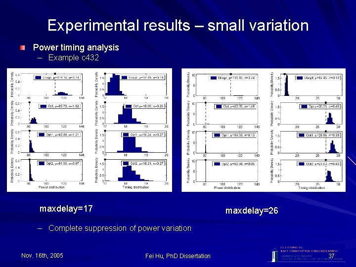
Experimental results – small variation Power timing analysis – Example c 432 maxdelay=17 maxdelay=26 – Complete suppression of power variation Nov. 16 th, 2005 Fei Hu, Ph. D Dissertation 37

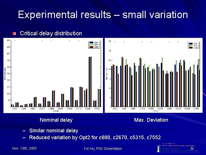
Experimental results – small variation Critical delay distribution Nominal delay Max. Deviation – Similar nominal delay – Reduced variation by Opt 2 for c 880, c 2670, c 5315, c 7552 Nov. 16 th, 2005 Fei Hu, Ph. D Dissertation 38

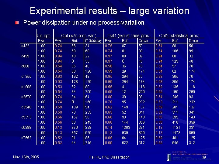
Experimental results – large variation Power dissipation under no process-variation Un-opt. c 432 c 499 c 880 c 1355 c 1908 c 2670 c 3540 c 5313 c 6288 c 7552 Pwr. 1. 00 1. 00 Nov. 16 th, 2005 Opt (w/o proc var. ) Opt 1 (worst case proc) Pwr. Buf. maxdelay Pwr. Buf. Dmax 0. 74 0. 94 0. 54 0. 93 0. 53 0. 54 0. 74 0. 59 0. 56 0. 13 0. 52 66 58 48 0 35 30 192 128 62 34 34 9 139 78 167 53 870 857 91 44 34 68 22 33 48 120 80 200 64 160 94 235 98 245 228 620 86 215 0. 74 0. 97 0. 58 0. 59 0. 95 0. 96 0. 55 0. 56 0. 80 0. 78 0. 62 0. 65 0. 66 0. 60 0. 14 0. 13 0. 69 0. 60 87 81 88 0 36 29 264 41 12 39 95 149 52 93 144 1303 939 64 622 Fei Hu, Ph. D Dissertation 50 99 32 48 70 174 116 290 93 232 137 341 143 356 331 899 125 312 Opt 2 (statistical proc) Pwr. 0. 74 0. 94 0. 54 0. 93 0. 52 0. 74 0. 73 0. 59 0. 55 0. 13 0. 52 Buf. 88 106 88 129 57 62 305 135 190 249 211 281 311 399 418 1121 1473 481 645 Dmax 50 99 32 48 70 174 116 290 93 232 137 341 143 356 331 899 125 312 39

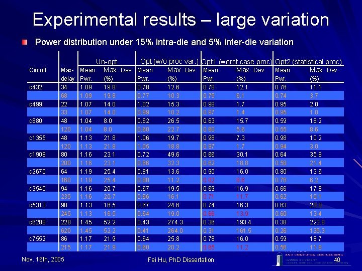
Experimental results – large variation Power distribution under 15% intra-die and 5% inter-die variation Circuit c 432 c 499 c 880 c 1355 c 1908 c 2670 c 3540 c 5313 c 6288 c 7552 Opt (w/o proc var. ) Opt 1 (worst case proc) Opt 2 (statistical proc) Un-opt Max- Mean Max. Dev. delay 34 68 22 33 48 120 80 200 64 160 94 235 98 245 228 620 86 215 Nov. 16 th, 2005 Pwr. 1. 09 1. 07 1. 04 1. 13 1. 16 1. 19 1. 16 1. 13 1. 45 1. 17 (%) 19. 8 14. 0 8. 0 21. 8 23. 1 25. 4 20. 7 16. 5 52. 2 21. 9 Pwr. 0. 78 0. 77 1. 02 0. 99 0. 62 0. 60 1. 06 1. 05 0. 72 0. 66 0. 81 0. 80 0. 67 0. 66 0. 67 0. 64 0. 43 0. 41 0. 64 0. 60 (%) 12. 6 10. 3 15. 3 10. 2 26. 5 22. 7 19. 7 18. 8 49. 6 32. 3 13. 6 11. 2 19. 5 16. 1 24. 6 19. 0 274. 3 264. 0 25. 8 20. 2 Pwr. 0. 78 0. 75 0. 98 0. 97 0. 63 0. 60 0. 98 0. 97 0. 66 0. 62 0. 90 0. 82 0. 69 0. 71 0. 74 0. 66 0. 31 0. 78 0. 65 Fei Hu, Ph. D Dissertation (%) 12. 1 6. 1 1. 7 1. 4 15. 7 5. 6 7. 3 1. 7 30. 1 18. 8 16. 0 8. 6 16. 9 11. 7 16. 3 13. 9 193. 4 161. 5 16. 0 11. 2 Pwr. 0. 76 0. 74 0. 95 0. 59 0. 55 0. 98 0. 94 0. 64 0. 58 0. 80 0. 76 0. 62 0. 63 0. 60 0. 38 0. 26 0. 59 0. 56 (%) 11. 1 3. 7 2. 0 18. 2 8. 6 10. 2 3. 0 35. 8 21. 4 13. 6 6. 2 17. 8 10. 1 20. 8 13. 4 223. 8 125. 3 18. 7 11. 8 40

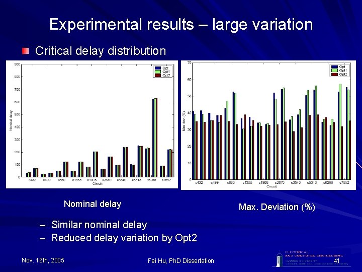
Experimental results – large variation Critical delay distribution Nominal delay Max. Deviation (%) – Similar nominal delay – Reduced delay variation by Opt 2 Nov. 16 th, 2005 Fei Hu, Ph. D Dissertation 41

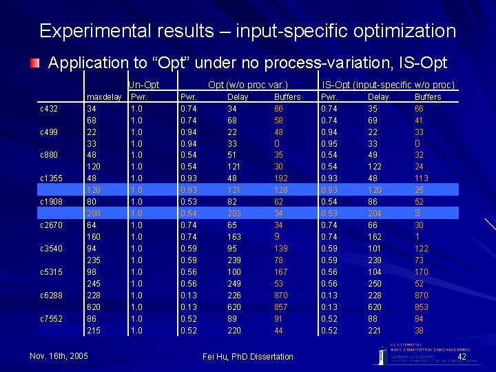
Experimental results – input-specific optimization Application to “Opt” under no process-variation, IS-Opt Un-Opt c 432 c 499 c 880 c 1355 c 1908 c 2670 c 3540 c 5315 c 6288 c 7552 maxdelay 34 68 22 33 48 120 80 200 64 160 94 235 98 245 228 620 86 215 Nov. 16 th, 2005 Pwr. 1. 0 1. 0 Opt (w/o proc var. ) Pwr. 0. 74 0. 94 0. 54 0. 93 0. 53 0. 54 0. 74 0. 59 0. 56 0. 13 0. 52 Delay 34 68 22 33 51 121 48 121 82 203 65 163 95 239 100 249 226 620 89 220 Buffers 66 58 48 0 35 30 192 128 62 34 34 9 139 78 167 53 870 857 91 44 Fei Hu, Ph. D Dissertation IS-Opt (input-specific w/o proc) Pwr. 0. 74 0. 94 0. 95 0. 54 0. 93 0. 54 0. 53 0. 74 0. 59 0. 56 0. 13 0. 52 Delay 35 69 22 33 49 122 48 120 86 204 66 162 101 239 104 250 228 620 88 221 Buffers 66 41 33 0 32 24 113 25 52 3 30 1 122 73 170 52 870 853 84 38 42

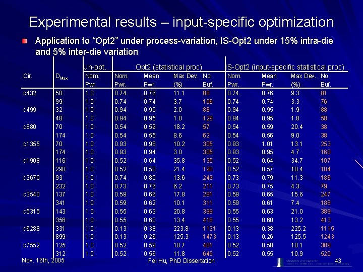
Experimental results – input-specific optimization Application to “Opt 2” under process-variation, IS-Opt 2 under 15% intra-die and 5% inter-die variation Un-opt. Cir. c 432 DMax 50 99 c 499 32 48 c 880 70 174 c 1355 70 174 c 1908 116 290 c 2670 93 232 c 3540 137 341 c 5315 143 356 c 6288 331 899 c 7552 125 312 Nov. 16 th, 2005 Nom. Pwr. 1. 0 1. 0 Opt 2 (statistical proc) Nom. Pwr. 0. 74 0. 94 0. 54 0. 93 0. 52 0. 74 0. 73 0. 59 0. 55 0. 13 0. 52 Mean Max Dev. No. Pwr. (%) Buf. 0. 76 11. 1 88 0. 74 3. 7 106 0. 95 2. 0 88 0. 95 1. 0 129 0. 59 18. 2 57 0. 55 8. 6 62 0. 98 10. 2 305 0. 94 3. 0 305 0. 64 35. 8 135 0. 58 21. 4 190 0. 80 13. 6 249 0. 76 6. 2 211 0. 66 17. 8 281 0. 62 10. 1 311 0. 63 20. 8 399 0. 60 13. 4 418 0. 38 223. 8 1121 0. 26 125. 3 1473 0. 59 18. 7 481 0. 56 11. 8 645 Fei Hu, Ph. D Dissertation IS-Opt 2 (input-specific statistical proc) Nom. Pwr. 0. 74 0. 94 0. 54 0. 93 0. 52 0. 73 0. 59 0. 55 0. 13 0. 52 Mean Pwr. 0. 76 0. 74 0. 95 0. 59 0. 56 1. 01 0. 95 0. 64 0. 57 0. 79 0. 75 0. 61 0. 63 0. 60 0. 38 0. 26 0. 58 0. 55 Max Dev. (%) 9. 3 3. 3 1. 9 1. 8 20. 4 9. 0 13. 1 4. 7 34. 7 18. 4 11. 3 4. 3 15. 6 7. 4 21. 0 13. 2 225. 2 125. 5 18. 1 10. 9 No. Buf. 81 76 88 58 38 38 253 160 107 104 186 79 247 188 389 413 1115 1243 389 520 43

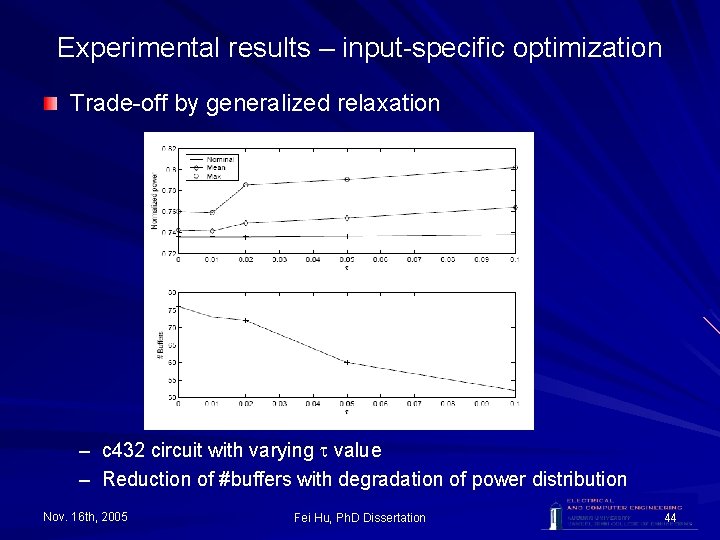
Experimental results – input-specific optimization Trade-off by generalized relaxation – c 432 circuit with varying value – Reduction of #buffers with degradation of power distribution Nov. 16 th, 2005 Fei Hu, Ph. D Dissertation 44

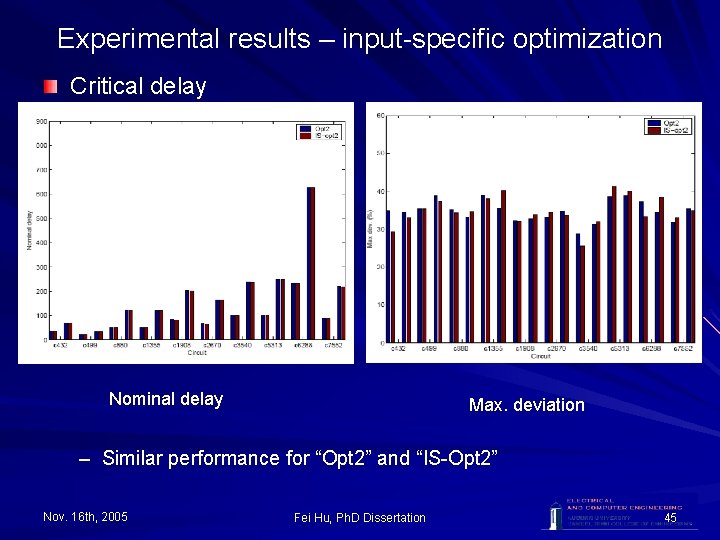
Experimental results – input-specific optimization Critical delay Nominal delay Max. deviation – Similar performance for “Opt 2” and “IS-Opt 2” Nov. 16 th, 2005 Fei Hu, Ph. D Dissertation 45

Outline Introduction Background – Dynamic power dissipation – Glitch reduction – Previous LP model Process-variation-resistant LP model – – Process variation Delay model LP model based on worst-case timing LP model based on statistical timing Input-specific optimization – Without process-variation – With process-variation Experimental results Conclusion Nov. 16 th, 2005 Fei Hu, Ph. D Dissertation 46

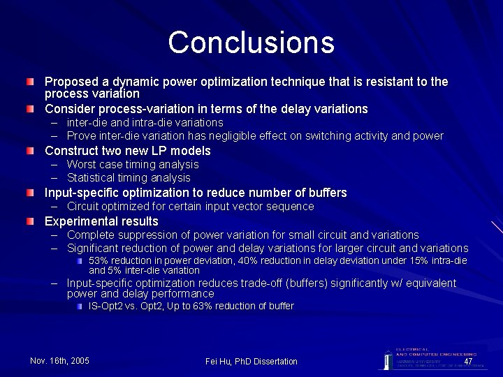
Conclusions Proposed a dynamic power optimization technique that is resistant to the process variation Consider process-variation in terms of the delay variations – inter-die and intra-die variations – Prove inter-die variation has negligible effect on switching activity and power Construct two new LP models – Worst case timing analysis – Statistical timing analysis Input-specific optimization to reduce number of buffers – Circuit optimized for certain input vector sequence Experimental results – Complete suppression of power variation for small circuit and variations – Significant reduction of power and delay variations for larger circuit and variations 53% reduction in power deviation, 40% reduction in delay deviation under 15% intra-die and 5% inter-die variation – Input-specific optimization reduces trade-off (buffers) significantly w/ equivalent power and delay performance IS-Opt 2 vs. Opt 2, Up to 63% reduction of buffer Nov. 16 th, 2005 Fei Hu, Ph. D Dissertation 47

Questions For more questions, contact me at hufei 01@auburn. edu Nov. 16 th, 2005 Fei Hu, Ph. D Dissertation 48