Process Variation Modeling Impact and Reduction Techniques Yu

- Slides: 41

Process Variation: Modeling, Impact and Reduction Techniques Yu Ching Chang Sabiha Hasan 1 ®

References • Impact of Die-to-Die and Within-Die Parameter Fluctuations on the Maximum Clock Frequency Distribution for Gigascale Integration by Keith A Bowman, Steven G. Duval 1 , James D. Meindl. Georgia Institute of Technology, Atlanta GA. 1 Intel Corp. Santa Clara, CA. • Parameter Variations and Impact on Circuits and Microarchitecture by Shekhar Borkar, Tanay Karnik, Siva Narendra, James Tschanz, Ali Keshavarzi, Vivek De. Circuit Research, Intel Labs. 2

Impact of Die-to-Die and Within. Die Parameter Fluctuations on the Maximum Clock Frequency Distribution for Gigascale Integration 3

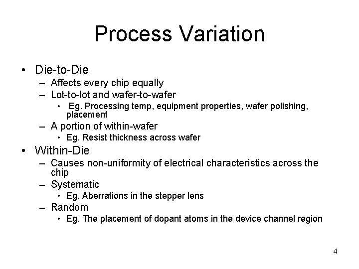
Process Variation • Die-to-Die – Affects every chip equally – Lot-to-lot and wafer-to-wafer • Eg. Processing temp, equipment properties, wafer polishing, placement – A portion of within-wafer • Eg. Resist thickness across wafer • Within-Die – Causes non-uniformity of electrical characteristics across the chip – Systematic • Eg. Aberrations in the stepper lens – Random • Eg. The placement of dopant atoms in the device channel region 4

The Impact of Process Variation • Over-estimation impacts the design effort – – Increase in design time Increase in die size Rejection of otherwise good designs Missed market window • Under-estimation impacts the manufacturing effort – Compromised product performance – Loss in overall yield – Increase in the silicon debug time 5

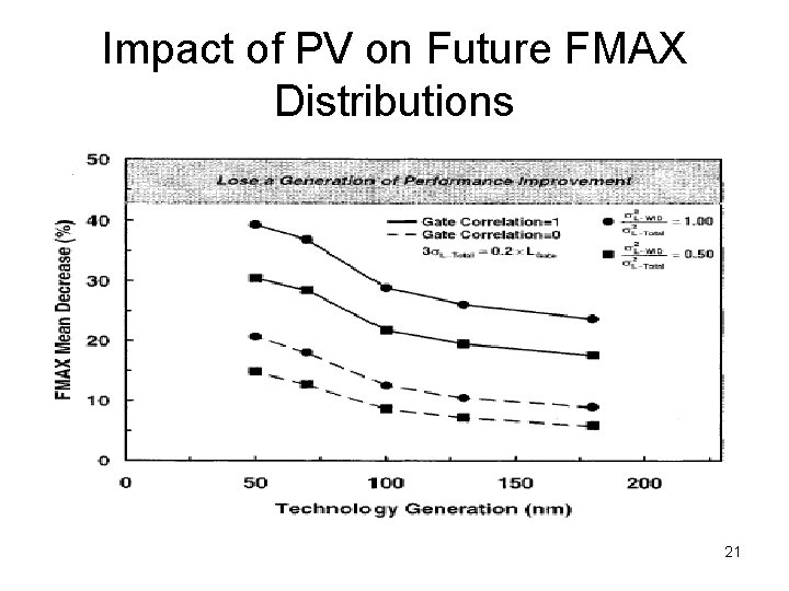
Contributions of the FMAX Distribution Model • Traditionally, die-to-die variations are the major concern, but as transistor feature size scales down, within-die variations become more and more significant • Both die-to-die and within-die parameter fluctuations significantly influence the FMAX distribution – Within-die primarily impacts the mean – Die-to-die determines the majority of FMAX variance • The model follows closely a wafer sort data for 0. 25 -μm microprocessor • The impact of parameter fluctuations is forecast for the 180, 130, 100, 70 and 50 -nm technology. 6

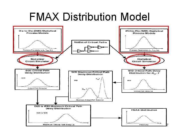
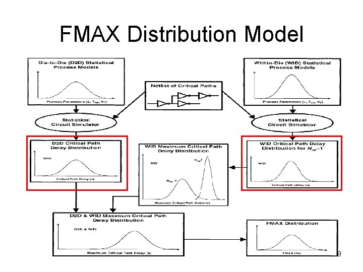
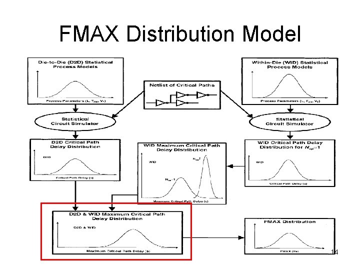
FMAX Distribution Model 7

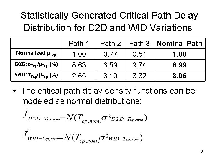
Statistically Generated Critical Path Delay Distribution for D 2 D and WID Variations Normalized μTcp D 2 D: σTcp/μTcp (%) WID: σTcp/μTcp (%) Path 1 1. 00 8. 63 2. 65 Path 2 0. 77 8. 59 3. 19 Path 3 Nominal Path 0. 51 1. 00 9. 74 8. 99 3. 32 3. 05 • The critical path delay density functions can be modeled as normal distributions: 8

FMAX Distribution Model 9

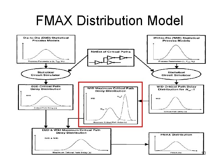
FMAX Distribution Model 10

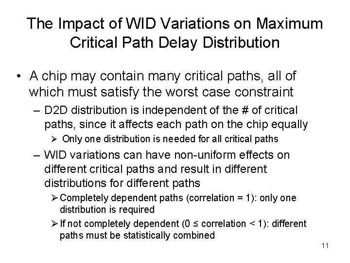
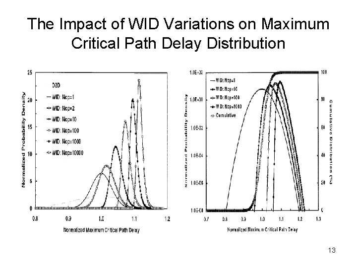
The Impact of WID Variations on Maximum Critical Path Delay Distribution • A chip may contain many critical paths, all of which must satisfy the worst case constraint – D 2 D distribution is independent of the # of critical paths, since it affects each path on the chip equally Ø Only one distribution is needed for all critical paths – WID variations can have non-uniform effects on different critical paths and result in different distributions for different paths Ø Completely dependent paths (correlation = 1): only one distribution is required Ø If not completely dependent (0 ≤ correlation < 1): different paths must be statistically combined 11

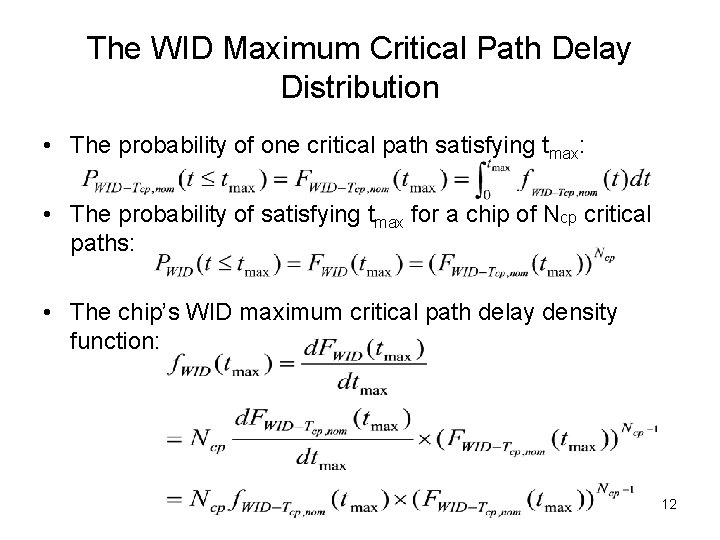
The WID Maximum Critical Path Delay Distribution • The probability of one critical path satisfying tmax: • The probability of satisfying tmax for a chip of Ncp critical paths: • The chip’s WID maximum critical path delay density function: 12

The Impact of WID Variations on Maximum Critical Path Delay Distribution 13

FMAX Distribution Model 14

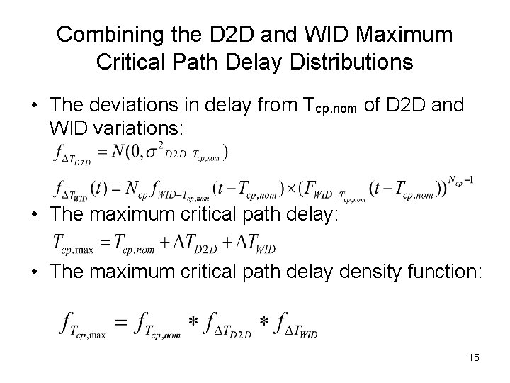
Combining the D 2 D and WID Maximum Critical Path Delay Distributions • The deviations in delay from Tcp, nom of D 2 D and WID variations: • The maximum critical path delay density function: 15

FMAX Distribution Model 16

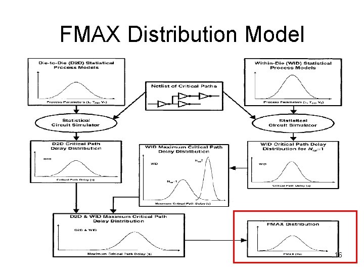
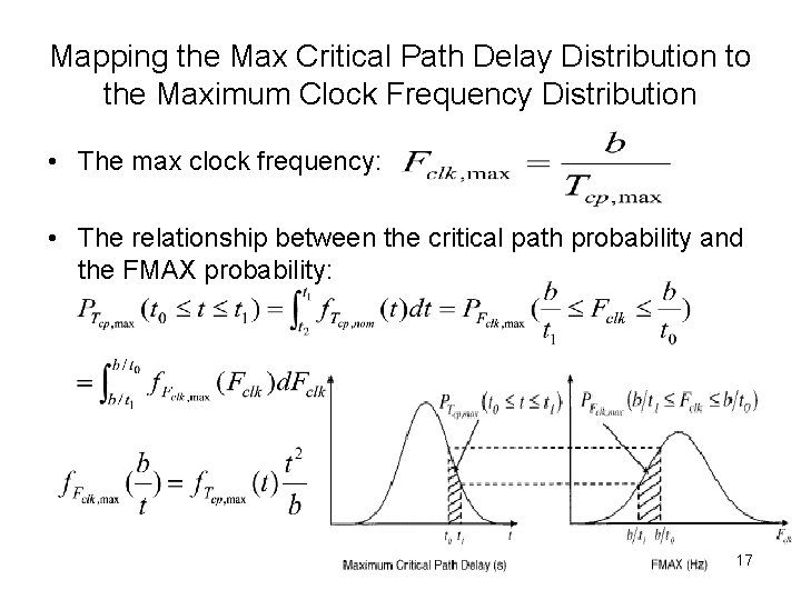
Mapping the Max Critical Path Delay Distribution to the Maximum Clock Frequency Distribution • The max clock frequency: • The relationship between the critical path probability and the FMAX probability: 17

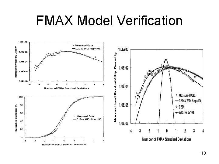
FMAX Model Verification 18

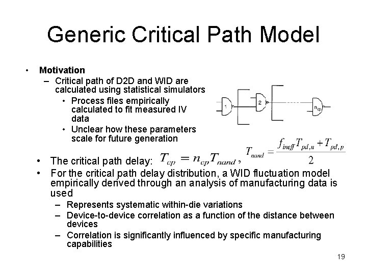
Generic Critical Path Model • Motivation – Critical path of D 2 D and WID are calculated using statistical simulators • Process files empirically calculated to fit measured IV data • Unclear how these parameters scale for future generation • The critical path delay: • For the critical path delay distribution, a WID fluctuation model empirically derived through an analysis of manufacturing data is used – Represents systematic within-die variations – Device-to-device correlation as a function of the distance between devices – Correlation is significantly influenced by specific manufacturing capabilities 19

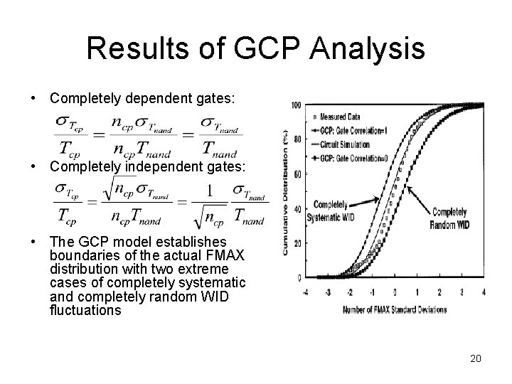
Results of GCP Analysis • Completely dependent gates: • Completely independent gates: • The GCP model establishes boundaries of the actual FMAX distribution with two extreme cases of completely systematic and completely random WID fluctuations 20

Impact of PV on Future FMAX Distributions 21

Summary • A model for maximum clock frequency (FMAX) distribution is presented • Model predictions agrees closely with measured data in mean, variance and shape • Model reveals that within-die variations primarily impact the FMAX mean while dieto-die variations the variance. 22

Outline • Variations – Process, supply voltage, and temperature • Impact of variations on circuits and microarchitecture • Variation tolerance and reduction – Process, circuit, and microarchitecture techniques • Summary 23

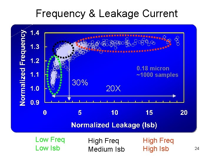
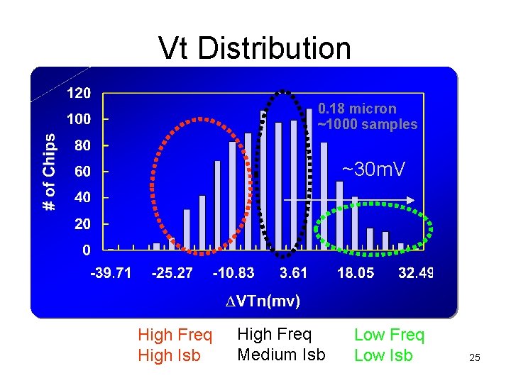
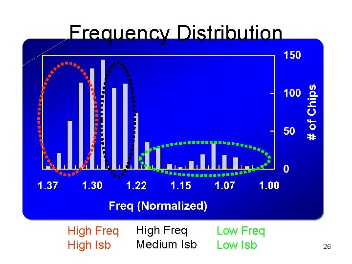
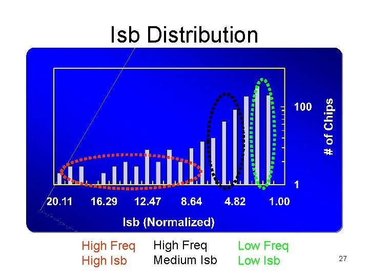
Frequency & Leakage Current 30% Low Freq Low Isb 0. 18 micron ~1000 samples 20 X High Freq Medium Isb High Freq High Isb 24

Vt Distribution 0. 18 micron ~1000 samples ~30 m. V High Freq High Isb High Freq Medium Isb Low Freq Low Isb 25

Frequency Distribution High Freq High Isb High Freq Medium Isb Low Freq Low Isb 26

Isb Distribution High Freq High Isb High Freq Medium Isb Low Freq Low Isb 27

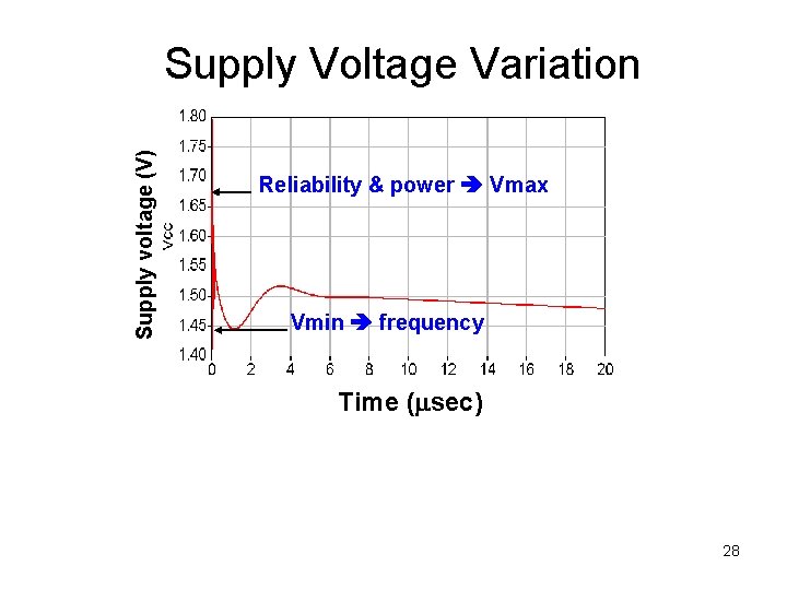
Supply voltage (V) Supply Voltage Variation Reliability & power Vmax Vmin frequency Time (msec) 28

Supply Voltage Variation • Max Vcc specified as a reliability limit for a process and Min Vcc is required for the target performance. • Variations in switching activity across the die and diversity of type of logic results in uneven power dissipation across the die -> results in uneven supply voltage distribution –> temperature hotspots across the die –> causing sub threshold leakage variation across the die. • Power delivery impedance does not scale with Vcc because packaging and platform technology. do not follow the scaling trend of the CMOS process. Therefore current delivery drops. • From the figure we see a droop in the voltage would lead to a degradation in performance. 29

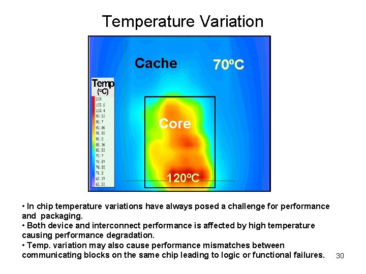
Temperature Variation Cache 70ºC Core 120ºC • In chip temperature variations have always posed a challenge for performance and packaging. • Both device and interconnect performance is affected by high temperature causing performance degradation. • Temp. variation may also cause performance mismatches between communicating blocks on the same chip leading to logic or functional failures. 30

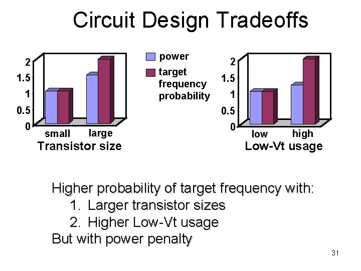
Circuit Design Tradeoffs power 2 target frequency probability 1. 5 1 0. 5 0 2 1. 5 1 0. 5 small large Transistor size 0 low high Low-Vt usage Higher probability of target frequency with: 1. Larger transistor sizes 2. Higher Low-Vt usage But with power penalty 31

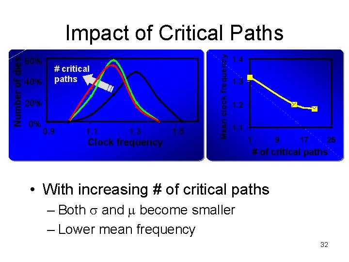
60% 40% # critical paths 20% 0% 0. 9 1. 1 1. 3 Clock frequency 1. 5 Mean clock frequency Number of dies Impact of Critical Paths 1. 4 1. 3 1. 2 1. 1 1 9 17 25 # of critical paths • With increasing # of critical paths – Both s and m become smaller – Lower mean frequency 32

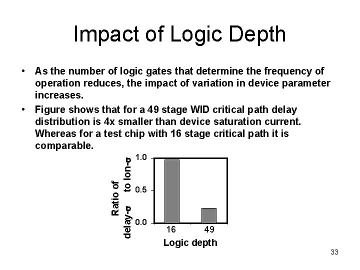
Impact of Logic Depth Ratio of delay-s to Ion-s • As the number of logic gates that determine the frequency of operation reduces, the impact of variation in device parameter increases. • Figure shows that for a 49 stage WID critical path delay distribution is 4 x smaller than device saturation current. Whereas for a test chip with 16 stage critical path it is comparable. 1. 0 0. 5 0. 0 16 49 Logic depth 33

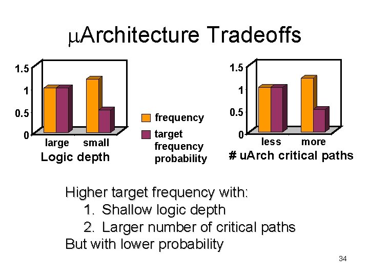
m. Architecture Tradeoffs 1. 5 1 1 0. 5 frequency 0 target frequency probability large small Logic depth 0. 5 0 less more # u. Arch critical paths Higher target frequency with: 1. Shallow logic depth 2. Larger number of critical paths But with lower probability 34

35

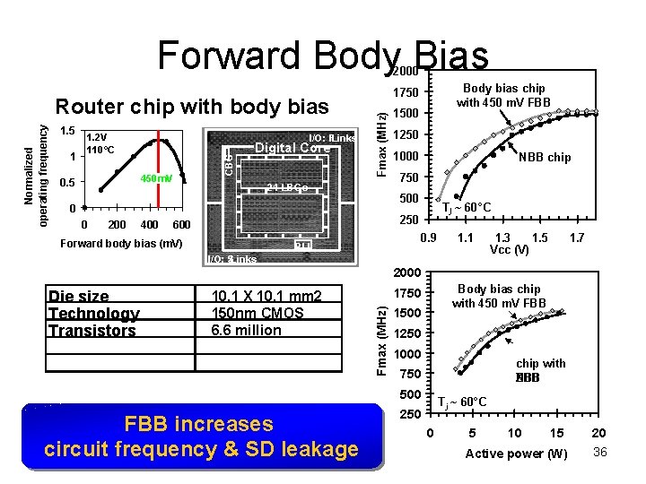
Forward Body Bias 2000 1 1. 2 V 110°C I/O: F -Links 450 m. V 0. 5 Digital Core Fmax (MHz) 1. 5 CBG Normalized operating frequency Router chip with body bias 24 LBGs 200 400 1500 1250 1000 NBB chip 750 500 0 0 Body bias chip with 450 m. V FBB 1750 Tj ~ 60°C 250 600 Forward body bias (m. V) 0. 9 PLL 1. 1 I/O: S -Links 1. 3 1. 5 Vcc (V) 1. 7 2000 10. 1 X 10. 1 mm 2 150 nm CMOS 6. 6 million Body bias chip with 450 m. V FBB 1750 Fmax (MHz) Die size Technology Transistors 1500 1250 1000 chip with NBB ZBB 750 500 FBB increases circuit frequency & SD leakage T j ~ 60°C 250 0 5 10 15 20 Active power (W) 36

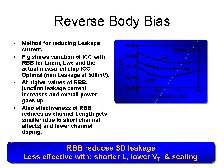
Reverse Body Bias • • • Method for reducing Leakage current. Fig shows variation of ICC with RBB for Lnom, Lwc and the actual measured chip ICC. Optimal (min Leakage at 500 m. V). At higher values of RBB, junction leakage current increases and overall power goes up. Also effectiveness of RBB reduces as channel Length gets smaller (due to short channel effects) and lower channel doping. 1 E-05 ICC (A) • 150 nm, 27 C 1 E-06 Lwc 1 E-07 1 E-08 1 E-09 0 Chip Lnom 0. 5 1 Reverse VBS (V) 1. 5 RBB reduces SD leakage Less effective with: shorter L, lower VT, & scaling 37

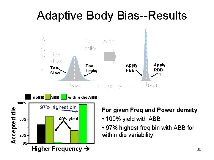
Adaptive Body Bias--Results no. BB Accepted die 100% 60% Too Slow Too Leaky ABB within die ABB 97% highest bin 100% yield Apply RBB For given Freq and Power density • 100% yield with ABB • 97% highest freq bin with ABB for within die variability 20% 0% Apply FBB Higher Frequency 38

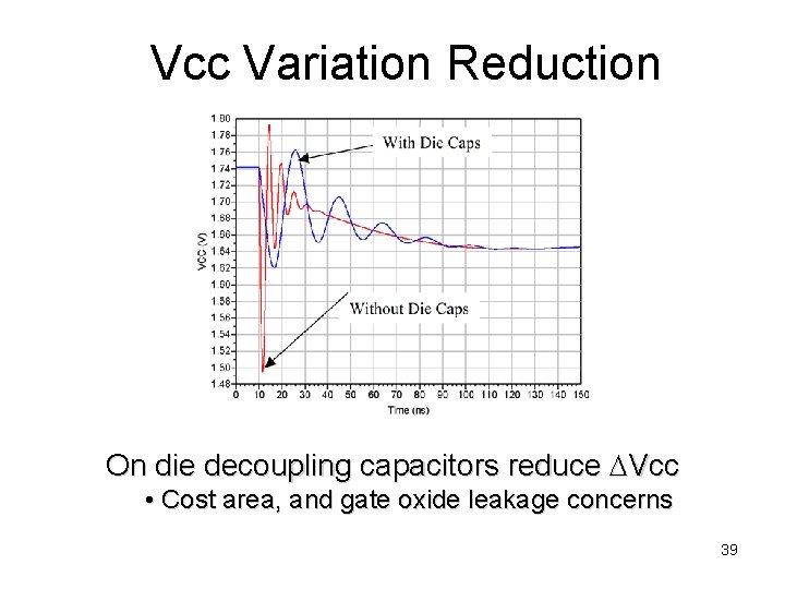
Vcc Variation Reduction On die decoupling capacitors reduce DVcc • Cost area, and gate oxide leakage concerns 39

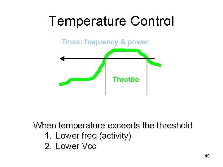
Temperature Control Tmax: frequency & power Throttle Time (usec) When temperature exceeds the threshold 1. Lower freq (activity) 2. Lower Vcc 40

Summary • Parameter variations will become worse with technology scaling. • Robust variation tolerant circuits and microarchitectures needed. • Multi-variable design optimizations considering parameter variations. • Major shift from deterministic to probabilistic design. 41