Process integration 2 double sided processing design rules

Process integration 2: double sided processing, design rules, measurements sami. franssila@aalto. fi
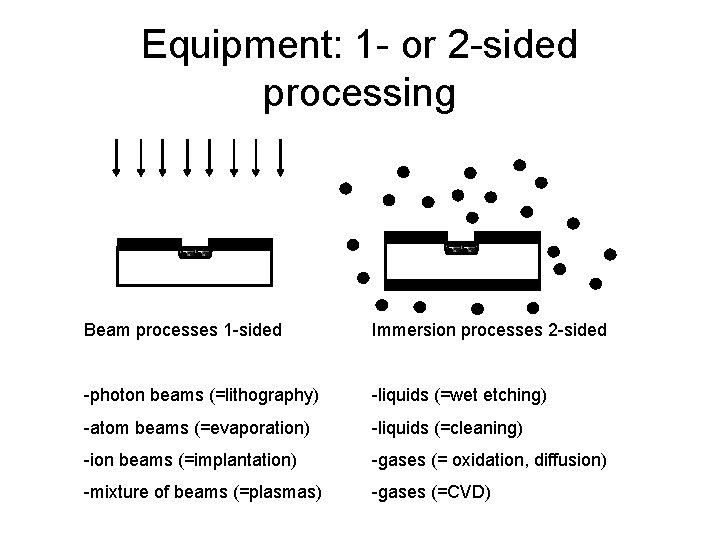
Equipment: 1 - or 2 -sided processing Beam processes 1 -sided Immersion processes 2 -sided -photon beams (=lithography) -liquids (=wet etching) -atom beams (=evaporation) -liquids (=cleaning) -ion beams (=implantation) -gases (= oxidation, diffusion) -mixture of beams (=plasmas) -gases (=CVD)

Double-sided processes Thermal oxidation CVD Wet etching Wet cleaning
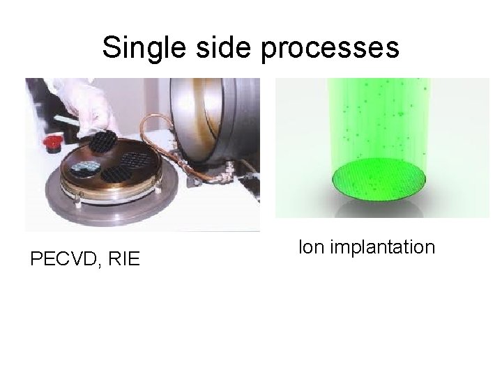
Single side processes PECVD, RIE Ion implantation

Wet etch vs. plasma etch Oxide wet etch in HF Oxide plasma etch in CHF 3 Film removed from backside Film remains on backside Undercutting etch profile Vertical sidewalls profile
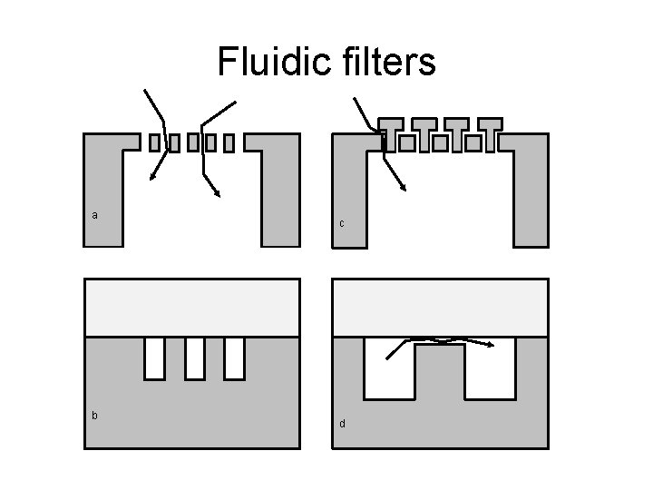
Fluidic filters a b c d

Cross section vs. layout view
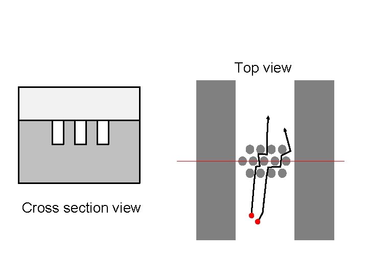
Top view Cross section view
Fluidic filters (2) Criteria: Need one or two wafers ? Cost, bonding. . . Pass size determined by litho ? Bonding ? Flow resistance ? Aperture ratio. Clogging ? Active cleaning ?
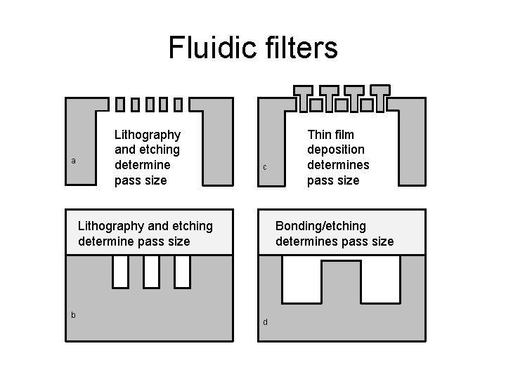
Fluidic filters a Lithography and etching determine pass size c Lithography and etching determine pass size b Thin film deposition determines pass size Bonding/etching determines pass size d
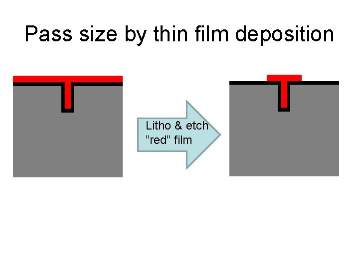
Pass size by thin film deposition Litho & etch ”red” film
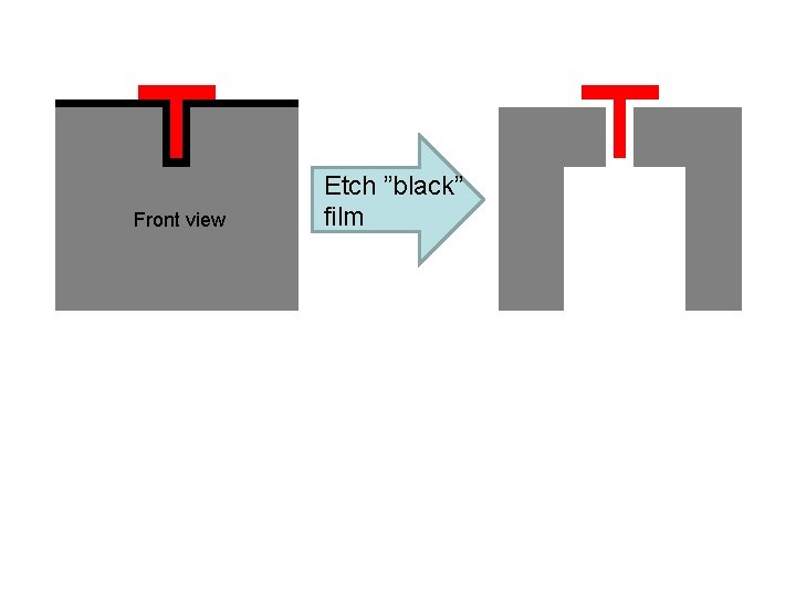
Front view Etch ”black” film

Alignment and design rules Example of Overlap rule: Coinciding structures must overlap by (LW/3)
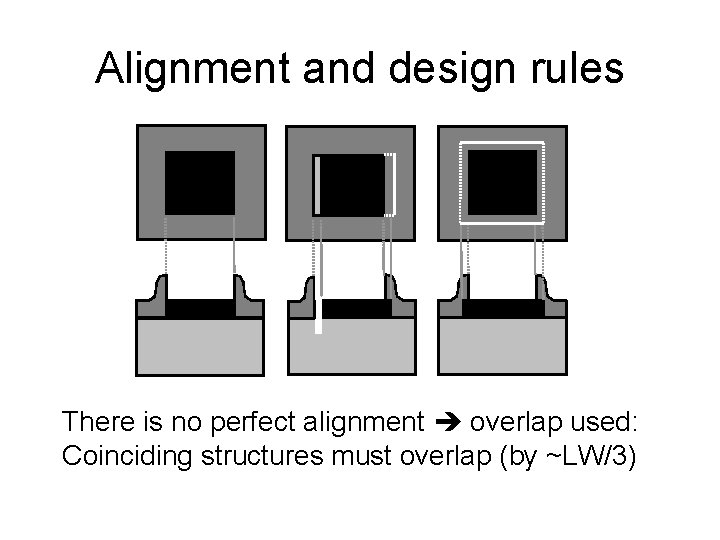
Alignment and design rules There is no perfect alignment overlap used: Coinciding structures must overlap (by ~LW/3)
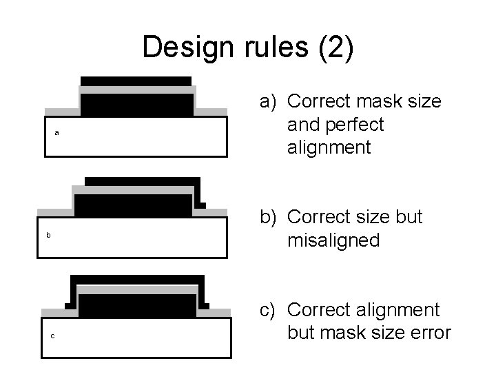
Design rules (2) a b c a) Correct mask size and perfect alignment b) Correct size but misaligned c) Correct alignment but mask size error

Design rules (3) Top electrode is made smaller than bottom electrode, to make sure that it lands on capacitor dielectric on planar area. Au-coil Capacitor area CVD ox-3 CVD ox-2 CVD ox-1 fused silica capacitor Mo resistor Si. Cr resistor nitride
Design rules (4) Minimum linewidth rule Minimum spacing rule Within one layer Initial assumption: minimum LW = minimum space Overlap rules for structures on different layers Breaking design rules ruins your process (=you are expecting too much from the process)
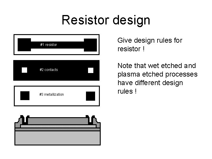
Resistor design #1 resistor #2 contactsholes #3 metallization Give design rules for resistor ! Note that wet etched and plasma etched processes have different design rules !
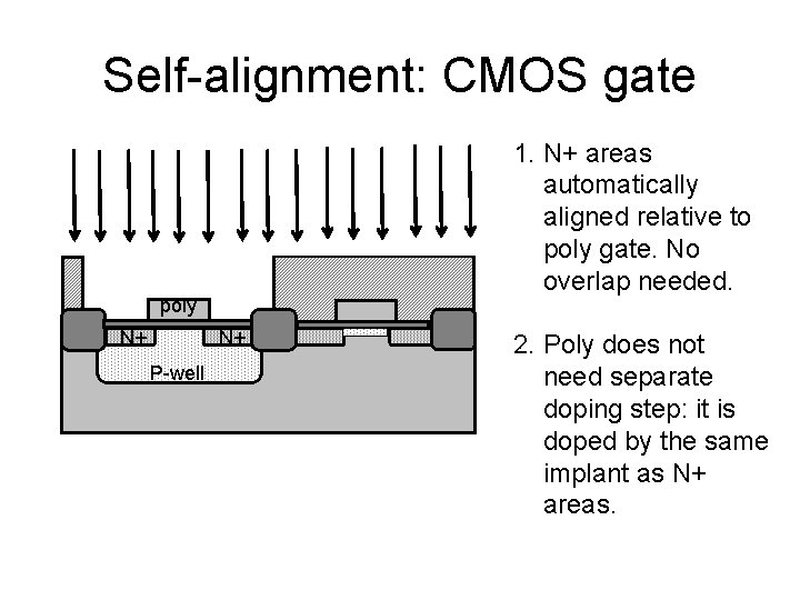
Self-alignment: CMOS gate 1. N+ areas automatically aligned relative to poly gate. No overlap needed. poly N+ N+ P-well 2. Poly does not need separate doping step: it is doped by the same implant as N+ areas.

Order of process steps
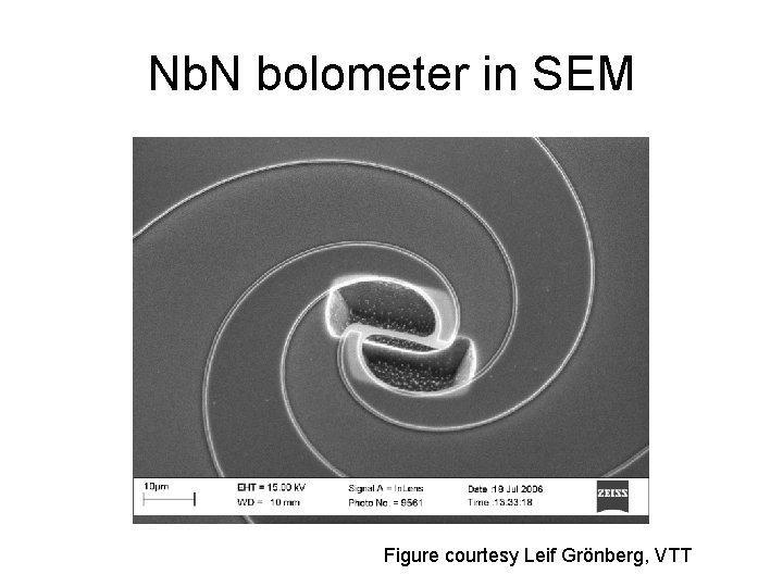
Nb. N bolometer in SEM Figure courtesy Leif Grönberg, VTT
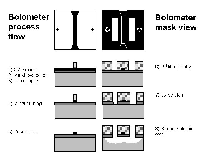
Bolometer process flow 1) CVD oxide 2) Metal deposition 3) Lithography Bolometer mask view 6) 2 nd lithography 7) Oxide etch 4) Metal etching 5) Resist strip 8) Silicon isotropic etch
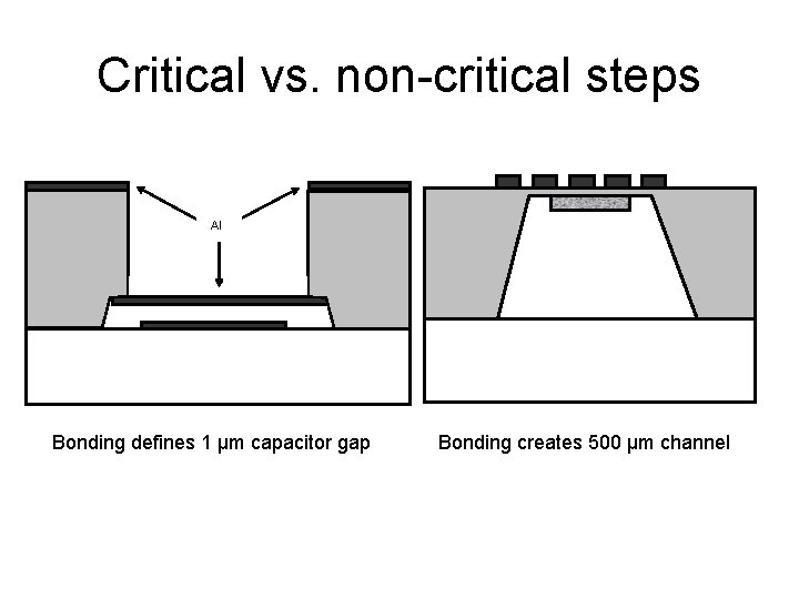
Critical vs. non-critical steps Al Bonding defines 1 µm capacitor gap Bonding creates 500 µm channel
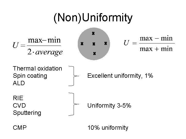
(Non)Uniformity Thermal oxidation Spin coating ALD Excellent uniformity, 1% RIE CVD Sputtering Uniformity 3 -5% CMP 10% uniformity
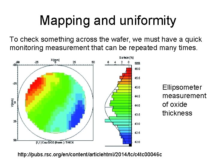
Mapping and uniformity To check something across the wafer, we must have a quick monitoring measurement that can be repeated many times. Ellipsometer measurement of oxide thickness http: //pubs. rsc. org/en/content/articlehtml/2014/tc/c 4 tc 00046 c
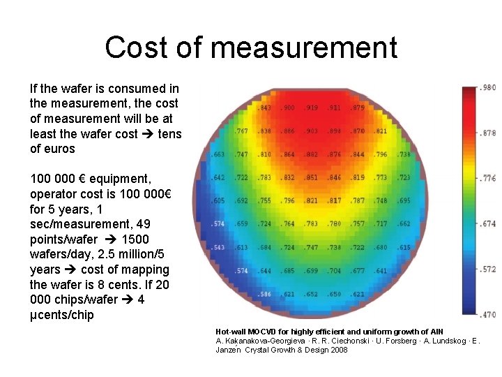
Cost of measurement If the wafer is consumed in the measurement, the cost of measurement will be at least the wafer cost tens of euros 100 000 € equipment, operator cost is 100 000€ for 5 years, 1 sec/measurement, 49 points/wafer 1500 wafers/day, 2. 5 million/5 years cost of mapping the wafer is 8 cents. If 20 000 chips/wafer 4 µcents/chip Hot-wall MOCVD for highly efficient and uniform growth of Al. N A. Kakanakova-Georgieva · R. R. Ciechonski · U. Forsberg · A. Lundskog · E. Janze n Crystal Growth & Design 2008
Film characterization needs -spatial resolution (image spot size) -depth resolution (surface vs. bulk properties) -elemental detection (constituents, impurities) -structural information (grain structure) -dimensional characterization (thickness) -mechanical properties (curvature, stress, …) -surface properties (roughness, reflectivity, …) -top view vs. cross sectional imaging -…
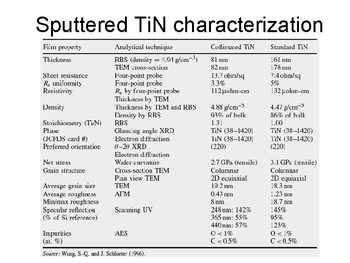
Sputtered Ti. N characterization
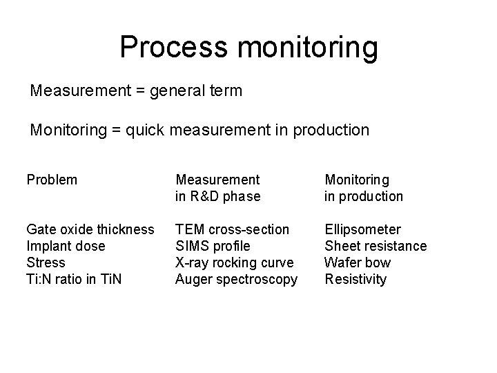
Process monitoring Measurement = general term Monitoring = quick measurement in production Problem Measurement in R&D phase Monitoring in production Gate oxide thickness Implant dose Stress Ti: N ratio in Ti. N TEM cross-section SIMS profile X-ray rocking curve Auger spectroscopy Ellipsometer Sheet resistance Wafer bow Resistivity
- Slides: 29