Process Errors in Integrated Circuits component e g



- Slides: 31

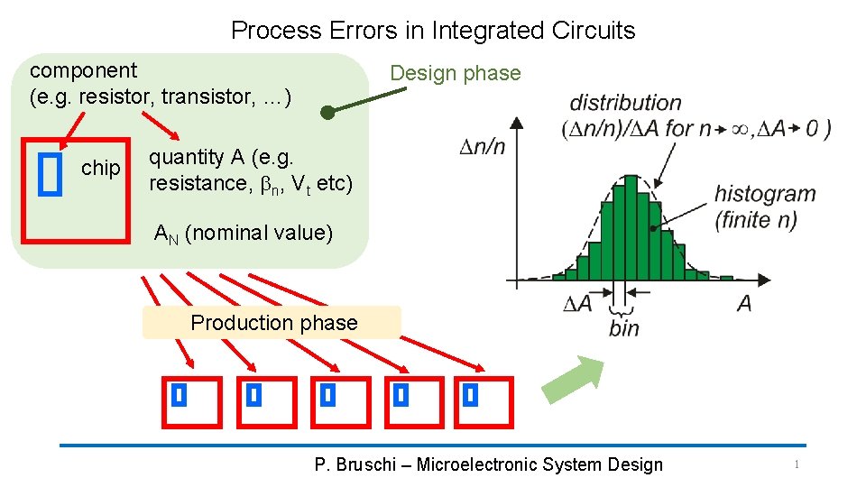
Process Errors in Integrated Circuits component (e. g. resistor, transistor, …) chip Design phase quantity A (e. g. resistance, bn, Vt etc) AN (nominal value) Production phase P. Bruschi – Microelectronic System Design 1

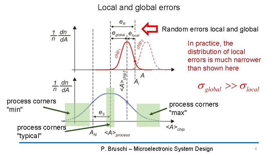
Components of the error and statistical representation s. A A N: nominal value Ai: A for a generic i-th component. <A>: the mean of the distribution. e S: Systematic error = <A>-AN e R: Random error for the i-th component e. R =Ai-<A>. Random error: standard deviation P. Bruschi – Microelectronic System Design 2

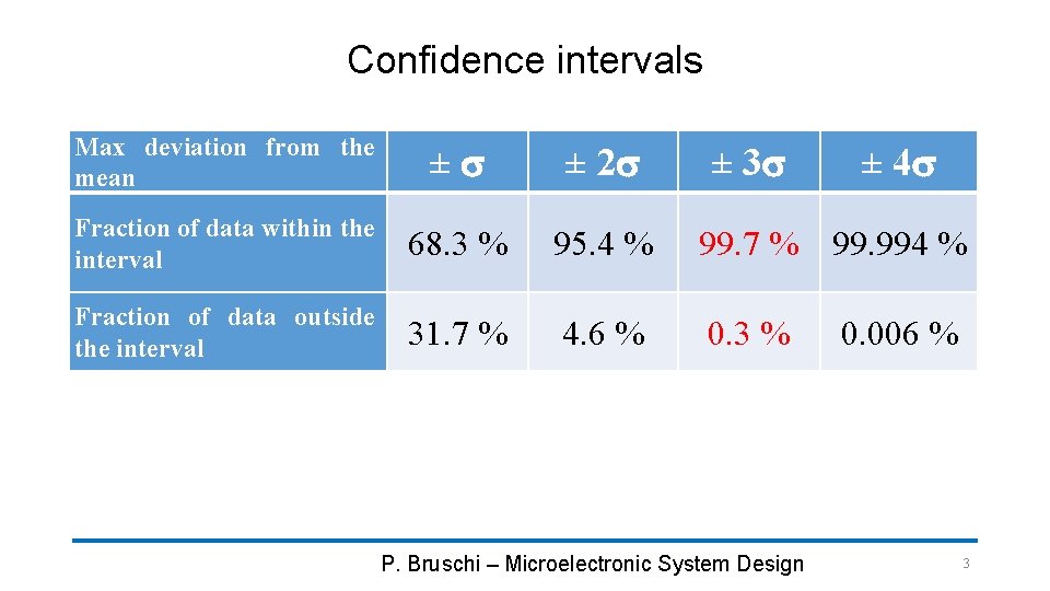
Confidence intervals Max deviation from the mean ±s ± 2 s Fraction of data within the interval 68. 3 % 95. 4 % 99. 7 % 99. 994 % Fraction of data outside the interval 31. 7 % 4. 6 % 0. 3 % ± 3 s P. Bruschi – Microelectronic System Design ± 4 s 0. 006 % 3

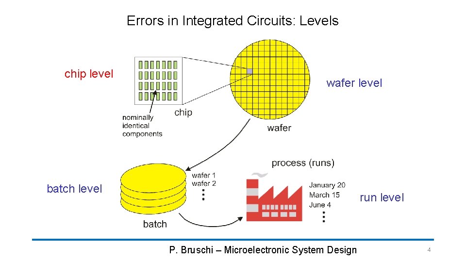
Errors in Integrated Circuits: Levels chip level wafer level batch level run level P. Bruschi – Microelectronic System Design 4

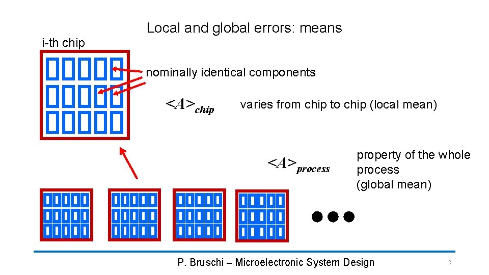
Local and global errors: means i-th chip nominally identical components <A>chip varies from chip to chip (local mean) <A>process property of the whole process (global mean) P. Bruschi – Microelectronic System Design 5

Local and global errors Random errors local and global In practice, the distribution of local errors is much narrower than shown here process corners "min" process corners "max" process corners "typical" P. Bruschi – Microelectronic System Design 6

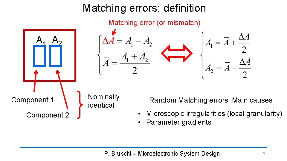
Matching errors: definition Matching error (or mismatch) A 1 A 2 Component 1 Component 2 Nominally identical Random Matching errors: Main causes • Microscopic irregularities (local granularity) • Parameter gradients P. Bruschi – Microelectronic System Design 7

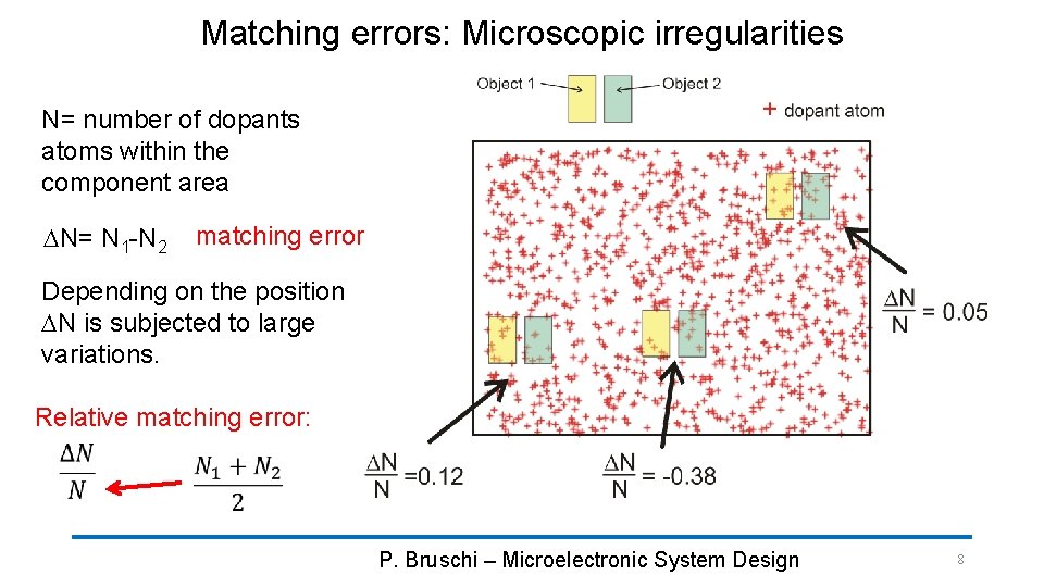
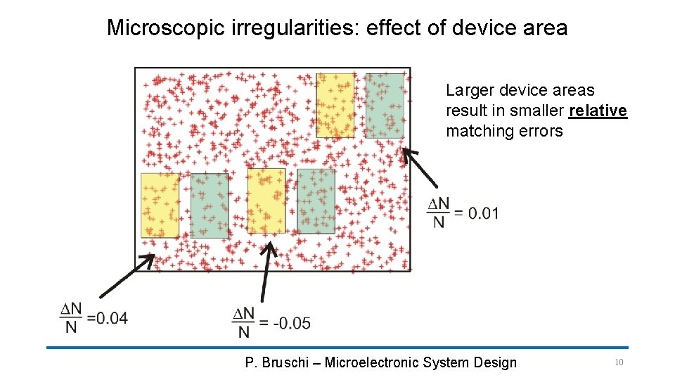
Matching errors: Microscopic irregularities N= number of dopants atoms within the component area DN= N 1 -N 2 matching error Depending on the position DN is subjected to large variations. Relative matching error: P. Bruschi – Microelectronic System Design 8

Matching errors: Microscopic irregularities • The number of dopants atoms affects several properties such as effective sheet resistance and MOSFET threshold voltage • The example can be replicated for other quantities, such as oxide thickness, where the crosses in the figure may represent local maxima or minima • The large fluctuation of DN/N can be ascribed to the small area of the devices shown in the example. For even smaller devices its is likely that one of the two devices does not include any dopant atom : DN/N may exceed unity (100 % error). P. Bruschi – Microelectronic System Design 9

Microscopic irregularities: effect of device area Larger device areas result in smaller relative matching errors P. Bruschi – Microelectronic System Design 10

Microscopic irregularities: the Pelgrom model Resistor Mosfet Cvt, Cb and CR are constant parameters of the process Their values are given in the Design Rule Manual, with names that depend on the foundry (there is no general convention). Cvt units are generally V·mm, while Cb and CR ones are mm. From: Pelgrom et a IEEE J. of Solid State Circuits, 1989 l P. Bruschi – Microelectronic System Design 11

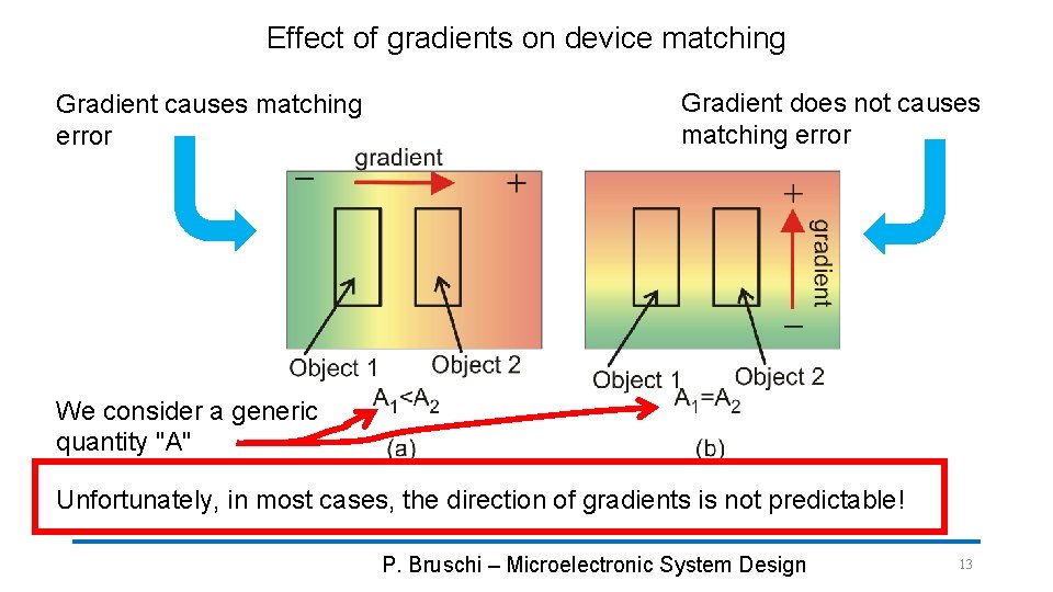
Matching Errors: Gradients • Gradients indicate that important quantities that affect the device properties are not uniformly distributed on a macroscopic scale. This means that these quantities gradually varies across the chip area. • Quantities of interest can be, for example: -) Dopant density -) Oxide thickness • -) Geometrical process biases (e. g. etching undercut) -) Temperature (e. g. due to power devices present on the chip) • -) Mechanical stress (mainly due to the packaging process) P. Bruschi – Microelectronic System Design 12

Effect of gradients on device matching Gradient causes matching error Gradient does not causes matching error We consider a generic quantity "A" Unfortunately, in most cases, the direction of gradients is not predictable! P. Bruschi – Microelectronic System Design 13

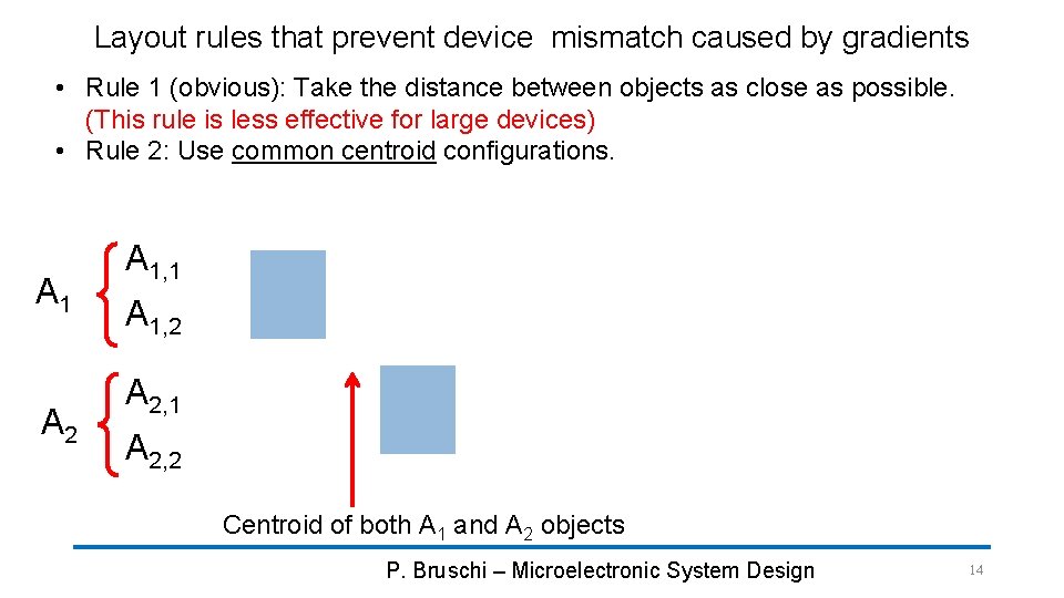
Layout rules that prevent device mismatch caused by gradients • Rule 1 (obvious): Take the distance between objects as close as possible. (This rule is less effective for large devices) • Rule 2: Use common centroid configurations. A 1 A 2 A 1, 1 A 1, 2 A 2, 1 A 2, 2 Centroid of both A 1 and A 2 objects P. Bruschi – Microelectronic System Design 14

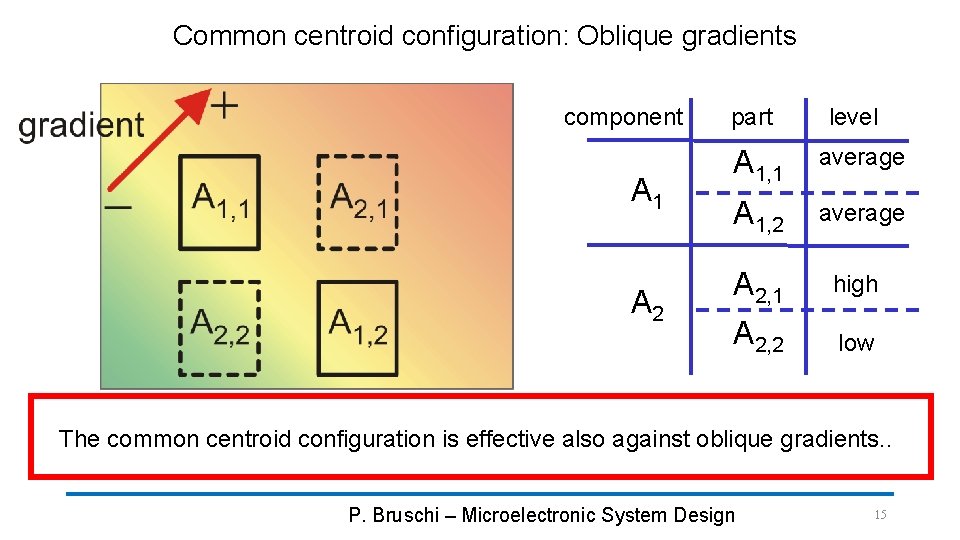
Common centroid configuration: Oblique gradients component A 1 A 2 part level A 1, 1 average A 1, 2 average A 2, 1 high A 2, 2 low The common centroid configuration is effective also against oblique gradients. . P. Bruschi – Microelectronic System Design 15

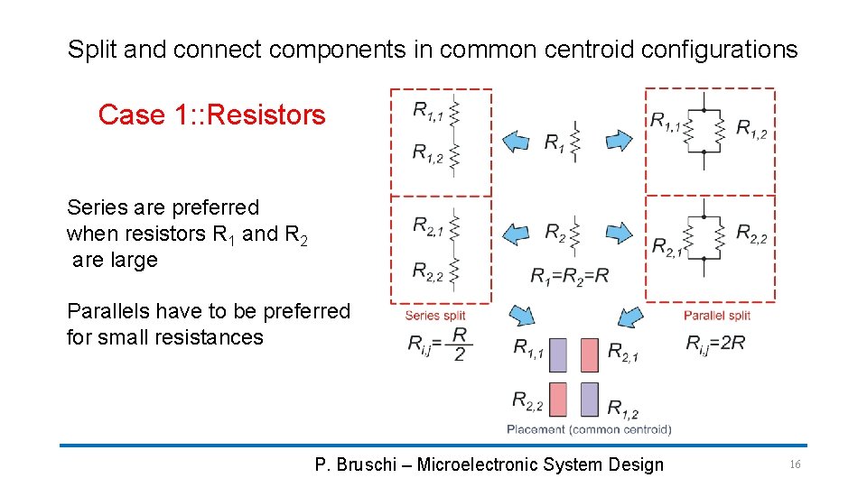
Split and connect components in common centroid configurations Case 1: : Resistors Series are preferred when resistors R 1 and R 2 are large Parallels have to be preferred for small resistances P. Bruschi – Microelectronic System Design 16

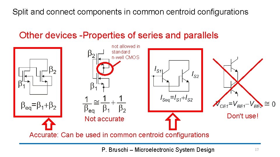
Split and connect components in common centroid configurations Other devices -Properties of series and parallels not allowed in standard n-well CMOS Not accurate Don't use! Accurate: Can be used in common centroid configurations P. Bruschi – Microelectronic System Design 17

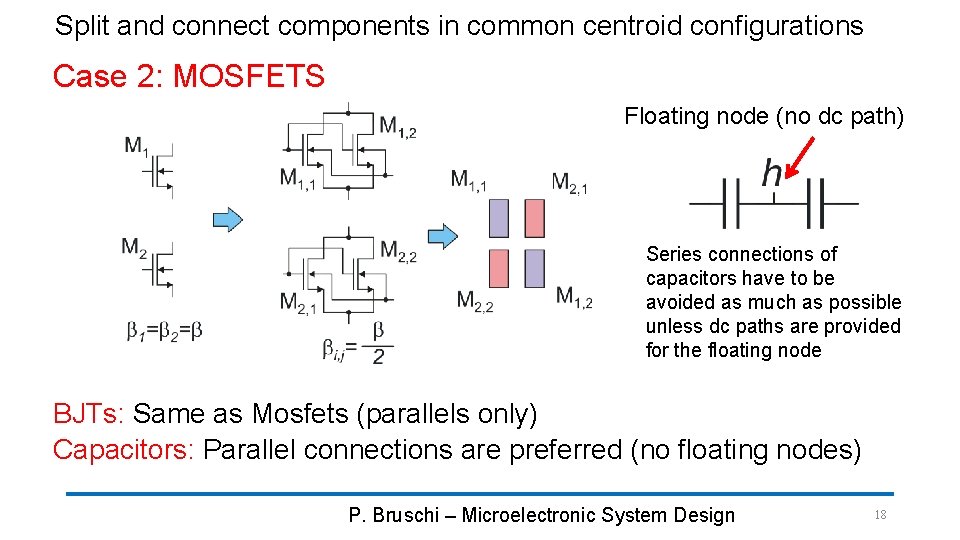
Split and connect components in common centroid configurations Case 2: MOSFETS Floating node (no dc path) Series connections of capacitors have to be avoided as much as possible unless dc paths are provided for the floating node BJTs: Same as Mosfets (parallels only) Capacitors: Parallel connections are preferred (no floating nodes) P. Bruschi – Microelectronic System Design 18

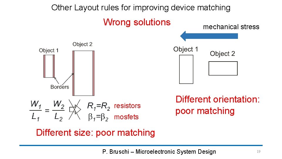
Other Layout rules for improving device matching Wrong solutions resistors mosfets mechanical stress Different orientation: poor matching Different size: poor matching P. Bruschi – Microelectronic System Design 19

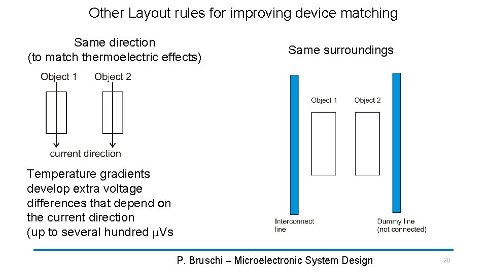
Other Layout rules for improving device matching Same direction (to match thermoelectric effects) Same surroundings Temperature gradients develop extra voltage differences that depend on the current direction (up to several hundred m. Vs P. Bruschi – Microelectronic System Design 20

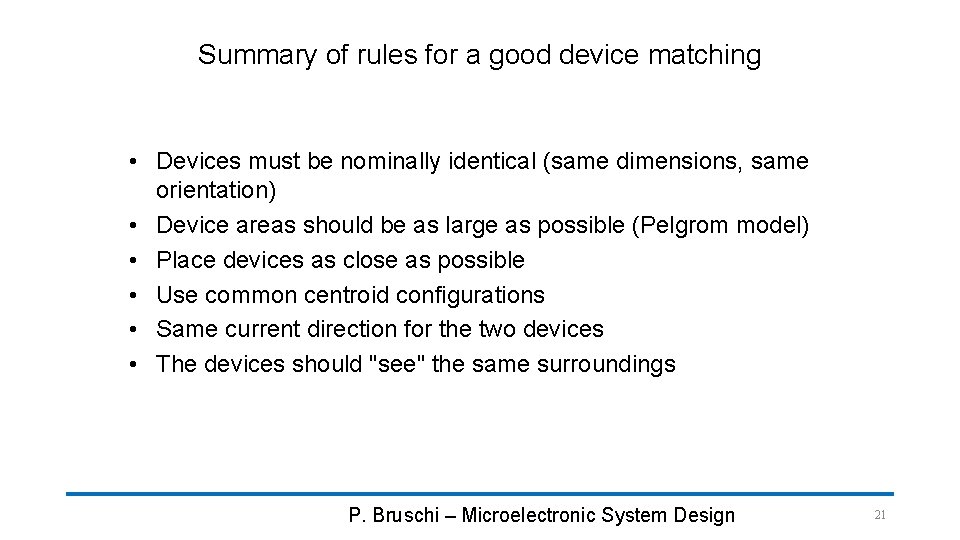
Summary of rules for a good device matching • Devices must be nominally identical (same dimensions, same orientation) • Device areas should be as large as possible (Pelgrom model) • Place devices as close as possible • Use common centroid configurations • Same current direction for the two devices • The devices should "see" the same surroundings P. Bruschi – Microelectronic System Design 21

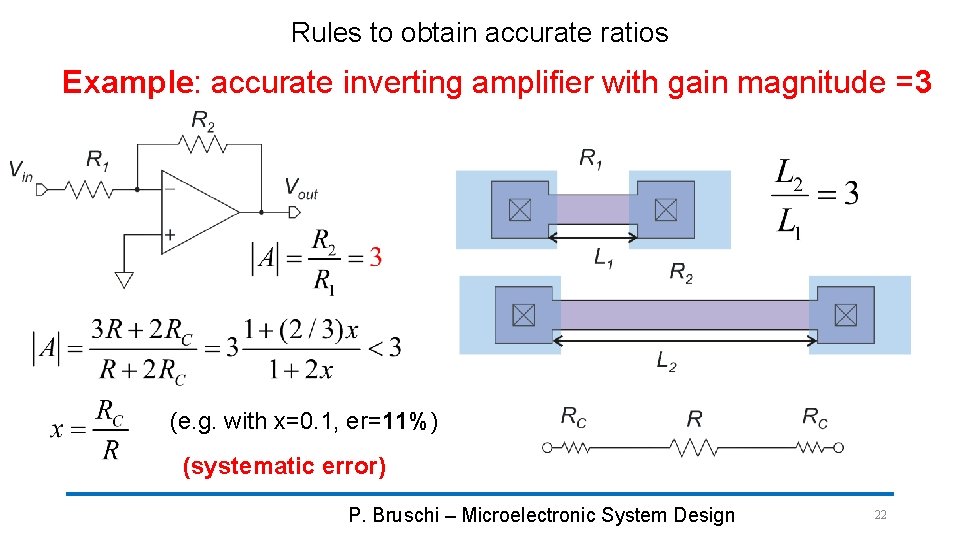
Rules to obtain accurate ratios Example: accurate inverting amplifier with gain magnitude =3 (e. g. with x=0. 1, er=11%) (systematic error) P. Bruschi – Microelectronic System Design 22

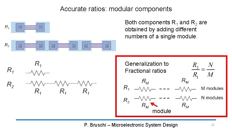
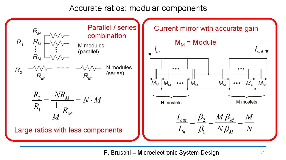
Accurate ratios: modular components Both components R 1 and R 2 are obtained by adding different numbers of a single module. Generalization to Fractional ratios module P. Bruschi – Microelectronic System Design 23

Accurate ratios: modular components Parallel / series combination Current mirror with accurate gain MM = Module Large ratios with less components P. Bruschi – Microelectronic System Design 24

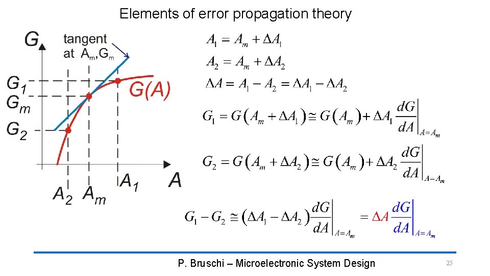
Elements of error propagation theory P. Bruschi – Microelectronic System Design 25

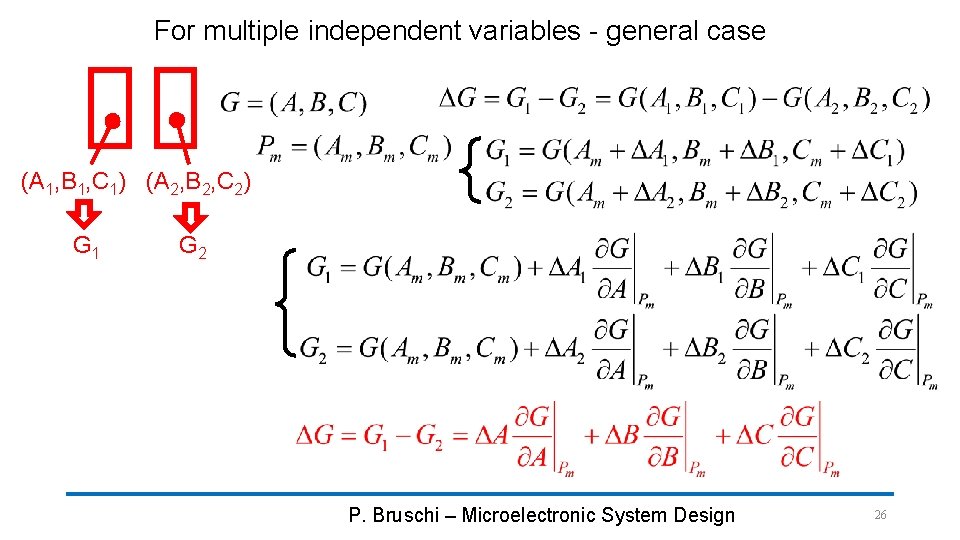
For multiple independent variables - general case (A 1, B 1, C 1) (A 2, B 2, C 2) G 1 G 2 P. Bruschi – Microelectronic System Design 26

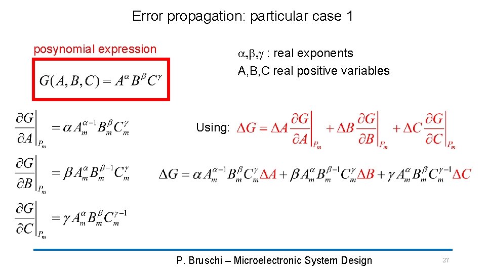
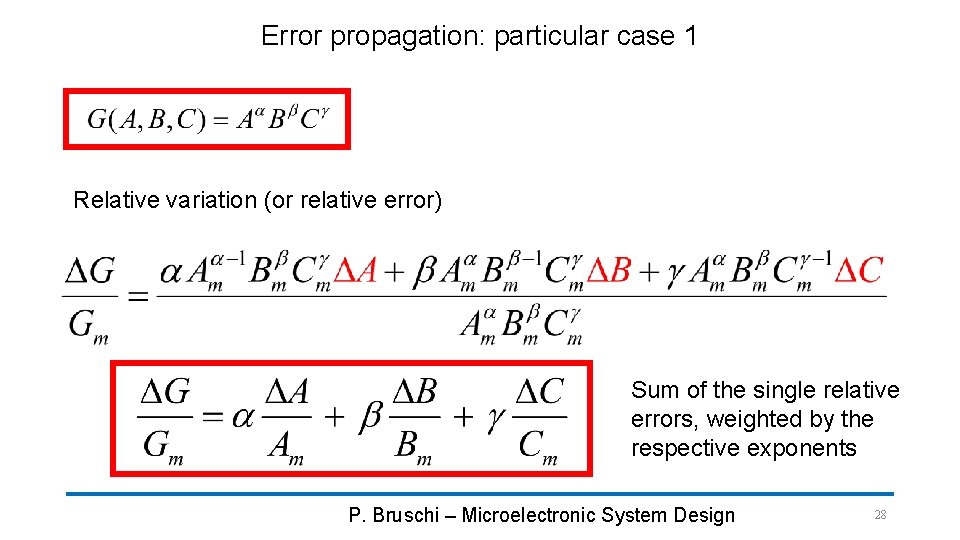
Error propagation: particular case 1 posynomial expression a, b, g : real exponents A, B, C real positive variables Using: P. Bruschi – Microelectronic System Design 27

Error propagation: particular case 1 Relative variation (or relative error) Sum of the single relative errors, weighted by the respective exponents P. Bruschi – Microelectronic System Design 28

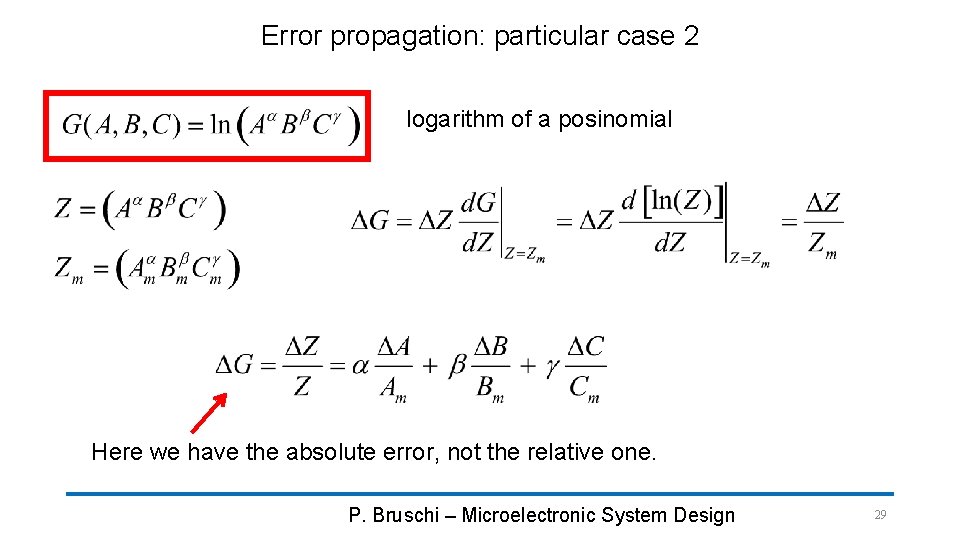
Error propagation: particular case 2 logarithm of a posinomial Here we have the absolute error, not the relative one. P. Bruschi – Microelectronic System Design 29

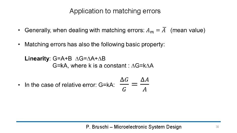
Application to matching errors P. Bruschi – Microelectronic System Design 30

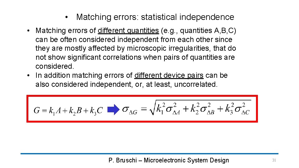
• Matching errors: statistical independence • Matching errors of different quantities (e. g. , quantities A, B, C) can be often considered independent from each other since they are mostly affected by microscopic irregularities, that do not show significant correlations when pairs of quantities are considered. • In addition matching errors of different device pairs can be also considered independent, or, at least, uncorrelated. P. Bruschi – Microelectronic System Design 31