Probe formation and basic image formation in SEM

Probe formation and basic image formation in SEM Using JEOL 5310 LV as example http: //virtual. itg. uiuc. edu/downloads/esemmanual. swf

Electrical currents in SEM column (those in red are or were part of the current that comes ‘boiling’ from the filament): CURRENTS filament heating current to heat filament and cause ‘boiling’ of e- off of tip (m. Amps-Amps AC) load current or emission current; gun current that doesn’t make it through the hole in the anode plate ‘lost’ at anode (μAmps-m. Amps) beam current; current in beam as it traverses column (p. Amps-m. Amps) (AC) (red arrows indicates direction of e- movement) Controls to effect and measure these currents: filament heating knob, gun bias, Acceleration Voltage

The Filament: Controls to effect and measure these currents: filament heating knob, gun bias, Acceleration Voltage

The Filament: Controls to effect and measure these currents: filament heating knob, gun bias, Acceleration Voltage

CURRENTS lens currents; current flowing through condenser and objective electron lenses and the scanning and stigmation coils to produce magnetic fields that steer or focus the e- beam (m. Amps) Controls to effect and measure these currents: condenser lens, objective lens, contrast, magnification, stigmator control,

In the e- lens, current through the windings creates a magnetic field, the pole piece is an important part of the lens design; it concentrates the field at the region where the focusing action is desired. A 100 e. V electron beam injected perpendicular to a dc magnetic field. The sense of the cyclotron orbit implies that the magnetic field points into the plane. Note that the beam light weakens with propagation distance For your information only; the fields that form the e- beam in the e- gun are electrostatic fields (also known as electric fields). The fields pictured on this slide (from current carrying coils) are magnetic fields. Ernst Ruska, credited with invention of the e- microscope, chose magnetic fields for his lenses due to practical, engineering concerns. There actually 2 pole pieces in an e- lens.

http: //www. globalsino. com/EM/page 4329. html

ELECTRON MICROSCOPES AS EXAMPLES OF PROJECTION VS. SCANNING IMAGING SYSTEMS electron source sample TEM Transmission em Image on electron sensitive projection screen SEM electron detector Scanning em Image produced on TV style monitor

condenser lens current constant, objective lens current changes objective lens current constant, condenser lens current changes alpha is convergence angle P is object distance (lens terminology) q is image distance (lens terminology) in this diagram q is the same as WD (working distance) d is spot diameter f is focal distance (variable; higher lens strength, shorter f, greater demagnification of spot, smaller spot) All beam current shown by the hatched lines is lost from the probe as it enters the column walls or apertures, the smaller the spot size, the more beam current is ‘lost’.

Electrical currents in SEM column (those in red are or were part of the current that comes ‘boiling’ from the filament): CURRENTS probe current; current in beam as it hits sample (p. AmpμAmps) sample current; current that leaves sample and enters SEM beam circuit through the column ‘ground’ (probe current minus secondary and backscattered e-) Controls to effect and measure these currents: aperture size, condenser lens, objective lens, magnification.
; this is the voltage that")
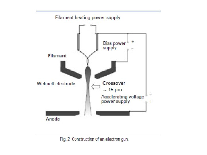
Voltages in SEM column : VOLTAGES acceleration voltage (ACCV); this is the voltage that defines the energy or velocity of the beam electrons and the energy of specimen emissions (usually 1000 V-30000 V, anode and column are positive relative to filament/cap). (AC) (red arrows indicates direction of e- movement) Gun bias voltage (all voltage is really a ‘bias’); voltage between filament and Wenhelt (gun) cap that shapes the e- beam at its origin and keeps the filament current in feedback at saturation (hundreds of V, cap is negative relative to filament). Controls: ACCV, gun bias,

emission from filament at e- gun W filament

Raster Pattern

Voltages in SEM Detector : VOLTAGES Faraday cage voltage; voltage relative to column or ‘ground’ that either draws, repels, or neither the secondary e- to/from the ET detector (-100 V - +300 V). The cage also prevents the field caused by the corona ring/scintillator face from distorting the beam. Scintillator face voltage; voltage relative to ground, metal coating on scintillator accelerates low energy secondary e- to induce light signal generation at the ET detector’s scintillator (‘phosphor’) surface (~+10000 V) PMT (photo multiplier tube) voltage relative to photocathode target at front of PMT; this is a gain voltage that multiplies the signal at the ET detector. For example a gain of 10 may give 10 counts out for each 1 e- in or 100 counts out for each 10 e- in. (+100 V - +1500 V). Control this V with contrast knob. SE-secondary e. PM-photomultiplier LG-light guide S-scintillator F-Faraday cage B-backscattered e. Controls: backscatter detector active, contrast control

PMT http: //cord. org/step_online/st 1 -6/st 16 eii 1. htm

How does energy travel through the SEM from gun to image? electrons - light - electrons - light beam - sample - scintillator - PM gain - other amps. - CRTbeam - CRT screen C = S 2 -S 1 / S 2 C% = (S 2 -S 1 / S 2 ) x 100 C is contrast of signal at sample S 2 & S 1 are signal at 2 points of interest at the sample where S 2>S 1 light Different types of signal are generated by sample/beam interaction and can be mapped by the SEM (MU does not have an Auger e- detector). This diagram of an ET detector (secondary e- detector) is only one of the detectors that can map signals from the sample/beam interaction. What other detectors can we use on the JEOL 5310 LV? Adapted from Goldstein 2003 In the graph at right, each line represents a beam current that is capable of generating an image. Beam current correlates with spot size (high beam current=large probe diameter). This graph shows how inherently low sample contrast can be overcome by slowing scan speed or raising beam current. What is a cathode ray (as in CRT)?

e- beam of constant ACCV Si Co SEM variables that allow us to increase signal differences given an inherent sample contrast (probe current and dwell time) Absolute difference (Co Si signal Co signal minus Si)in # of Se- that can be (Se- per location or pixel) multiplied by the ET PMT probe current = 1 n. A or 6. 25 x 109 e- / second fast scan dwell time = 0. 1 second slow scan dwell time = 1 second 5 x 10⁹ 5 x 10¹⁰ 6. 25 x 109 6. 25 x 1010 probe current = 1 u. A or 6. 25 x 1012 e- / second fast scan dwell time = 0. 1 second slow scan dwell time = 1 second 5 x 10¹² 5 x 10¹³ 1. 25 x 1012 6. 25 x 1012 1. 25 x 1013 6. 25 x 1013 1. 25 x 109 1. 25 x 1010 Inherent sample contrast (these are convenient numbers, not true values for Si and Co) These are 2 sample locations, location 1 is Si, location 2 is Co. Lets say that when a single beam e- hits Si it generates 8 Se-, when it hits Co, it generates 10 Se-. What is the inherent contrast in terms of Se- of these 2 sample locations. C = S 2 -S 1 / S 2 C% = (S 2 -S 1 / S 2 ) x 100 CSi/Co = 10 -8 / 10 =. 2 or 20% IN WORDS ONE COULD SAY, “GIVEN SAMPLE CONTRAST OF 1% AND BEAM CURRENT OF 1 n. A, WE NEED A FRAME TIME OF AT LEAST 600 SECONDS TO DIFFERENTIATE 2 SAMPLE LOCATIONS. ” or , “GIVEN SAMPLE CONTRAST OF 1% AND FRAME TIME OF 100 SECONDS, WE NEED A BEAM CURRENT OF ~10 n. A OR MORE, TO DIFFERENTIATE 2 SAMPLE LOCATIONS. ” dwell time = frame time / pixel # = # of sample locations being probed and displayed

The Everhart-Thornley SE detector SE-secondary e. PM-photomultiplier LG-light guide S-scintillator F-Faraday cage B-backscattered e- +300 V (relative to ground) SE -50 V (relative to ground) Adapted from Goldstein

Electron penetration trajectories in a typical SEM beam acceleration voltage varied (10, 20, & 30 k. V), same sample. acc. V constant, carbon at left, iron at right

Elastic and inelastic events in EM, a beam e- can lose its kinetic energy in many different events, each of these is, at least in part, a quantized transfer A 30 k. V ELECTRON CANNOT GENERATE A 31 k. V SIGNAL • Elastic: backscattered electrons are beam electrons that scatter at angles up to 90 degrees from initial beam trajectory (by definition >50 e. V) • Inelastic: secondary e- (continuous energy distribution by definition <50 e. V) x-ray production: continuum (bremsstrahlung or braking) or characteristic Auger e- are of specific energies based on elemental composition (like characteristic x-rays) these are not quantitatively measured in our JEOL 5310 LV SEM visible light fluorescence (cathodoluminescence)

Diagram from JEOL 5310 LV; A, B, & C are solid state BSE detectors. A and B are overhead detectors, C is a third detector that allows for ‘shadowing’ when imaging topography in BSE mode. + + + - BSE signal

all these occur both in SEM & TEM ‘e- emissions’ ‘braking x-radiation’ is emitted as e- are slowed by the fields around nuclei of material, this radiation increases with sample atomic # because larger nuclei lead to more dense Coulombic fields Goldstein, 1992

Characteristic x-ray production is defined by atomic orbital e- transitions Y axis is # of xray photons EKα = EK – EL Ekβ = EK-EM so EKα<Ekβ<EK<E beam e. EK or EM here is ionization energy, the energy difference between these = the observed x-ray energies Each of these lines can correspond to a peak in a spectrum like the one at left X axis is energy of xray photons braking radiation characteristic (elemental) x-ray peaks Can we can do x-ray spectroscopy in SEM? How about optical confocal microscope? Goldstein, 1992

e- beam Intrinsic region is also here after Li drifting during manufacture 2 D sample Cross sectional diagrams of silicon [Si(Li)] x-ray detector used in x-ray eds. These diagrams show two slightly different views. The intrinsic region of each detector is Li doped and is the region that counts x-rays by converting their energy into electron current. Normal P (boron doped) or N (phosphorus doped) type silicon is not a good x-ray detector because of excessive e- and hole current even in the absence of an x-ray event. e- beam 3 D X-rays The next 2 slides address spectral artifacts and how the EDS detector disperses the xray energies for plotting. sample

You will not be tested on this page but it may help you with other concepts. The Si detector and the escape peak: When an x-ray enters detector, it makes a charge pulse that is monitored. This pulse has size (total # of e- counts in detector) based on the formula: # of e- counts = Energyx-ray in e. V / ε’ (ε’ = 3. 8 e. V for Si, this is the energy needed to create an e-/hole pair in our detector, notice how low this value is, it must be a bonding (molecular) e-, not an inner shell e- that is involved) Usually, this energy is entirely captured by multiple electronic/kinetic events inside the detector. If it is not, say an inner shell Si electron is displaced and a Si K x-ray (1. 74 ke. V) is generated and escapes, now the pulse count does not accurately represent the energy of the incoming x-ray as some energy has escaped. This event causes us to see the ‘escape peak’ which is seen on our spectrum at 1. 74 ke. V below the actual incident x-ray energy peak of the sample. 8. 04 ke. V (Cu K) – 1. 74 ke. V (Si K) = 6. 3 ke. V (Cu K escape peak)

Top and bottom spectra are the same data, just different scaling. The electron beam was focused on the sem specimen stage which is made of a brass alloy; mostly copper and zinc. main Cu K peak (Kα) at 8. 04 ke. V ? Cu Kα escape peak Cu Kα sum peak Low beam current (30% dead time on detector) High beam current (60% dead time) Although these spectra show system peaks by definition (these are x-rays coming from part of our microscope chamber or the stage) we do not call them artifacts because we were intentionally focused and collecting signal from our sem stage. In this case, our system is our sample! Why does too much beam current lead to this copper ‘sum peak’ (far right arrow)? What is the apparent benefit of the higher beam current setting? Can you find the Cu escape peak? See lower right spectrum and look down energy from the very large Cu peak.

• End Intro to SEM

• Begin old copies of slides

Electrical currents in SEM column (those in red are or were part of the current that comes ‘boiling’ from the filament): CURRENTS filament heating current to heat filament and cause ‘boiling’ of e- off of tip (m. Amps-Amps AC) load current or emission current; gun current that doesn’t make it through the hole in the anode plate ‘lost’ at anode (μAmps-m. Amps) beam current; current in beam as it traverses column (p. Amps-m. Amps) probe current; current in beam as it hits sample (p. Amp-μAmps) sample current; current that leaves sample and enters SEM beam circuit through the column ‘ground’ (probe current minus secondary and backscattered e-) lens currents; current flowing through condenser and objective electron lenses and the scanning and stigmation coils to produce magnetic fields that steer or focus the e- beam (m. Amps) Controls to effect and measure these currents: filament heating knob, gun bias, ACCV, aperture size, condenser lens, objective lens, contrast, magnification, stigmator control, faraday cup with ammeter

Electrical currents in SEM column (those in red are or were part of the current that comes ‘boiling’ from the filament): CURRENTS filament heating current to heat filament and cause ‘boiling’ of e- off of tip (m. Amps-Amps AC) load current or emission current; gun current that doesn’t make it through the hole in the anode plate ‘lost’ at anode (μAmps-m. Amps) beam current; current in beam as it traverses column (p. Amps-m. Amps) probe current; current in beam as it hits sample (p. AmpμAmps) sample current; current that leaves sample and enters SEM beam circuit through the column ‘ground’ (probe current minus secondary and backscattered e-) lens currents; current flowing through condenser and objective electron lenses and the scanning and stigmation coils to produce magnetic fields that steer or focus the e- beam (m. Amps) Controls to effect and measure these currents: filament heating knob, gun bias, ACCV, aperture size, condenser lens, objective lens, contrast, magnification, stigmator control, faraday cup with ammeter
; this is the voltage that")
Voltages in SEM column : VOLTAGES acceleration voltage (ACCV); this is the voltage that defines the energy or velocity of the beam electrons and the energy of specimen emissions (usually 1000 V-30000 V, anode and column are positive relative to filament/cap). Gun bias voltage (all voltage is really a ‘bias’); voltage between filament and Wenhelt (gun) cap that shapes the e- beam at its origin and keeps the filament current in feedback at saturation (hundreds of V, cap is negative relative to filament). Faraday cage voltage; voltage relative to column or ‘ground’ that either draws, repels, or neither the secondary e- to/from the ET detector (-100 V - +300 V). The cage also prevents the field caused by the corona ring/scintillator face from distorting the beam. Scintillator face voltage; voltage relative to ground, metal coating on scintillator accelerates low energy secondary e- to induce light signal generation at the ET detector’s scintillator (‘phosphor’) surface (~+10000 V) PMT (photo multiplier tube) voltage relative to photocathode target at front of PMT; this is a gain voltage that multiplies the signal at the ET detector. For example a gain of 10 may give 10 counts out for each 1 e- in or 100 counts out for each 10 e- in. (+100 V - +1500 V). Control this V with contrast knob. Controls: ACCV, gun bias, backscatter detector active, contrast control

Just for your information from SPI. • • SPI Tungsten Hairpin Brand Filaments and Electron Sources Some easy to understand comments about tungsten hairpin vs. La. B 6 sources for electron microscopes This is not intended to be a detailed description of how the electron sources in a microscope operate, but to outline the salient details. Detailed descriptions abound in the literature and various EM reference books (see for example. Reimer - Scanning Electron Microscopy Springer- Verlag 1985) The first thing to make clear is that the accelerating voltage of the microscope (HV) does not have a great deal to do with electron emission per se. There is an interaction of the filament, it's power supplies and the HV power supplies. This is due to the fact the filament and it's power supply must reside within the HV tank and operate while electrically floating at the high end of the HV terminal, also it is relevant to design the electronics to simplify operation and hence there is some interconnections between the HV and the bias voltages. The important point to keep in mind here is that the primary function of the HV is to accelerate the electrons into the electron optical column. The HV itself is not the source of the electron beam. It is the function of the filament to be the source of these electrons. There are 3 common types of electron sources in use today: Thermionic emission, Partial Field Emitters, and Pure Field Emitters. In the case of a thermal emitter, electrons are emitted from the hot material in accord with the Richardson equation for thermionic (heated) emission. The function of the filament (heater) current is to give the electrons in the source enough thermal energy to over come the energy barrier which is prohibiting their escape. All metals will give off electrons when heated and the higher the temperature the more electrons are emitted, however most materials do not survive very long at the temperatures required for this process to yield a significant amount of electrons. Tungsten (W) has a sufficiently high melting temperature (3650 K) that it survives for a longer time at elevated temperatures ( ~ 2600 - 3000 K) before it fails an it is the material of choice for a typical thermionic emitter. Another way to get emission is to decrease the "work function (energy barrier)" which is limiting emission. Materials with lower work functions emit at lower temperatures (La. B 6 for example). These materials are sometime referred to as partial field emitters since they exploit the fact that their reduced work function enables their operation at lower temperatures than W (~1400 -2000 K). The use of this "partial field emitter" nomenclature is not rigorously true, since the primary excitation mechanism is still thermal activation. Finally field emission sources operate due to a decrease of their energy barrier width by an applied field permitting quantum tunneling of electrons through the narrowed barrier into "vacuum". This is a different process all together than thermionic emission and is governed by the Fowler- Nordheim relations. There are two types of Field emitters - Thermally assisted (sometimes called Schottky) emitters and Cold Field Emitters. As the names imply, thermally assisted Field emitters are heated, while the Cold Field emitters are not, both require the application of an external field to "extract" the electron beam from a very small tip. The electrons which are emitted from the filament regardless of the type of emitter are "replaced" by virtue of the fact that there is a connection to ground and the electron reservoir in metals is a continuum, hence the filament remains overall neutral. If this ground connection was not present, the material would become in effect, locally charged, and the electron emission would start to decline, and eventually stop (the local energy barrier would continually increase). For the case of the Thermionic & La. B 6 Guns, the filament, wehnelt cap and anode from a triode system. By judicious design of the power supply the wehnelt is made slightly negative with the filament and the resulting the electrostatic field which acts as a small lens and produces a focussing of the electrons which are emitted only from a limited region of the hot tip of the W source. This voltage difference is usually called the "bias" voltage of the gun. In the Field emitters a multiple anode system is employed instead of the triode configuration. Here one applies an extraction voltage instead of the bias voltage. Bias voltages are usually a few hundred volts, while the extraction voltage on a FEG is usually in the range of 3 -5 k. V. The filament and wehnelt (or last anode for an FEG) are also connected to the negative terminal of the HV supply. Thus, the beam of electrons which leaves the wehnelt is accelerated by the HV toward the nearest grounded anode, which is judiciously placed at the base of the gun. This acceleration gives the electrons their Z (axial) velocity. Some of these electrons make it through a small aperture in the grounded anode which is the entrance to the electron column. Once past the final gun electrode (ie. the one at ground potential ) the Z acceleration of the electrons is essentially zero and they are traveling at constant velocity (determined by the HV) until they hit the sample. The function of the remaining lenses and deflectors in the body of the microscope are to further deflect/focus this beam onto the specimen in the manner chosen by the analyst. Lastly you should not that the electrons are emitted from a thermionic filament much the same way as they are in a light bulb. As in the case of the light bulb, failure of the filament is usually due to mass transfer/melting. This does involve movement of metal atoms away from the point of failure (even though you are below the melting point). Over heating the filament causes this to happen faster and thus decreased the filament life. The above information was taken from an E-mail reply drafted by Dr. Nestor Zaluzec to answer someone's question and we re-publish his E-mail comments here with minor editing for greater clarity. We wish to thank Dr. Zaluzec, Argonne National Laboratories for permitting us to use this short description of the differences in the workings of the different electron sources.
- Slides: 35