Principles of Instrumental Analysis Chapter 21 Surface Characterization
- Slides: 43

Principles of Instrumental Analysis Chapter 21 Surface Characterization by Spectroscopy and Microscopy

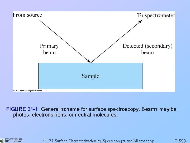
FIGURE 21 -1 General scheme for surface spectroscopy. Beams may be photos, electrons, ions, or neutral molecules. 歐亞書局 Ch 21 Surface Characterization by Spectroscopy and Microscopy P. 590

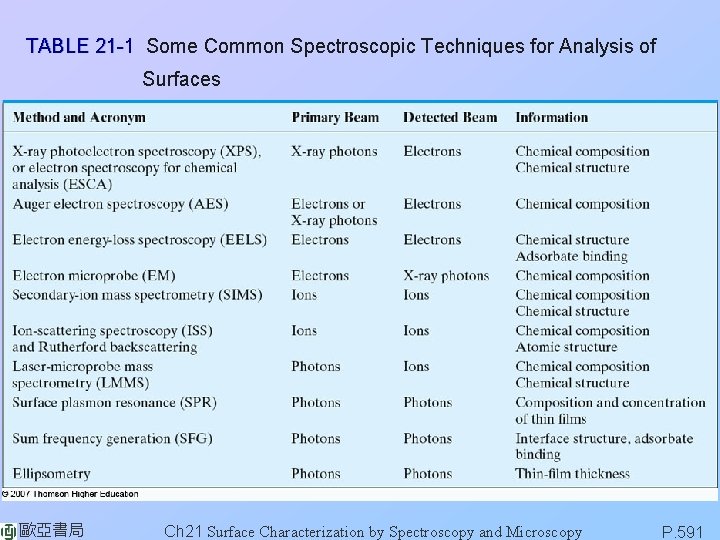
TABLE 21 -1 Some Common Spectroscopic Techniques for Analysis of Surfaces 歐亞書局 Ch 21 Surface Characterization by Spectroscopy and Microscopy P. 591

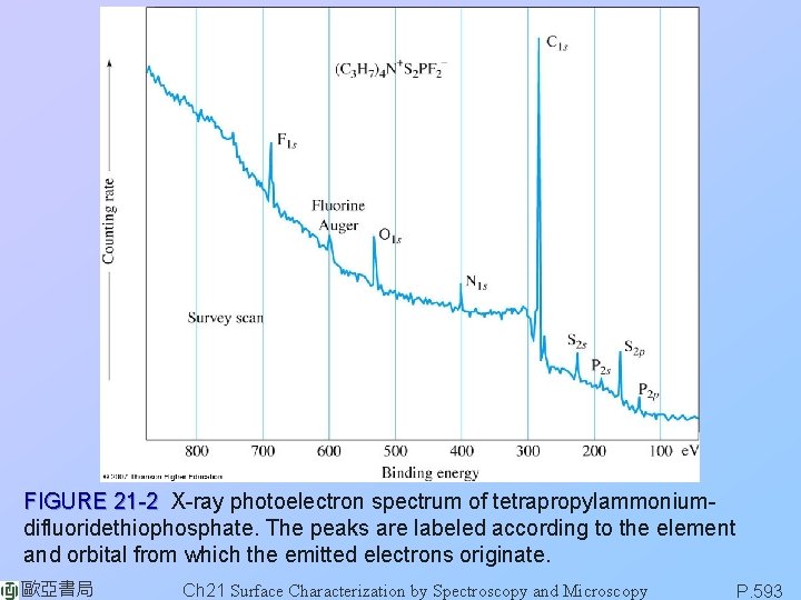
FIGURE 21 -2 X-ray photoelectron spectrum of tetrapropylammoniumdifluoridethiophosphate. The peaks are labeled according to the element and orbital from which the emitted electrons originate. 歐亞書局 Ch 21 Surface Characterization by Spectroscopy and Microscopy P. 593

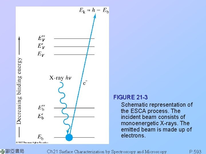
FIGURE 21 -3 Schematic representation of the ESCA process. The incident beam consists of monoenergetic X-rays. The emitted beam is made up of electrons. 歐亞書局 Ch 21 Surface Characterization by Spectroscopy and Microscopy P. 593

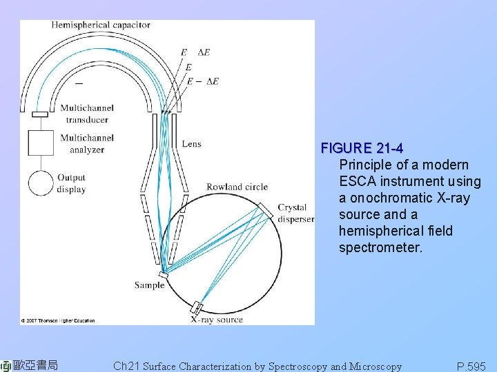
FIGURE 21 -4 Principle of a modern ESCA instrument using a onochromatic X-ray source and a hemispherical field spectrometer. 歐亞書局 Ch 21 Surface Characterization by Spectroscopy and Microscopy P. 595

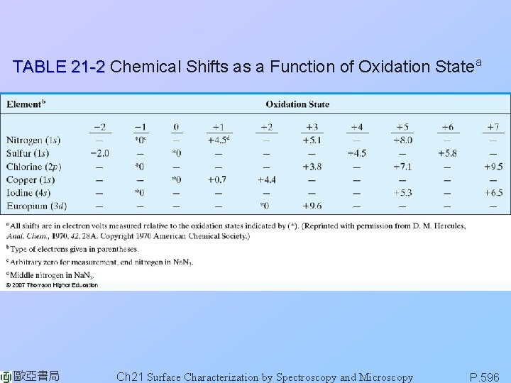
TABLE 21 -2 Chemical Shifts as a Function of Oxidation Statea 歐亞書局 Ch 21 Surface Characterization by Spectroscopy and Microscopy P. 596

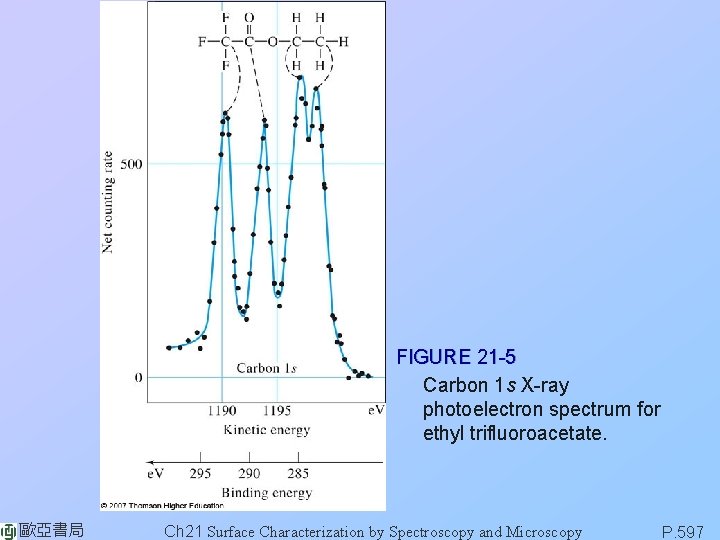
FIGURE 21 -5 Carbon 1 s X-ray photoelectron spectrum for ethyl trifluoroacetate. 歐亞書局 Ch 21 Surface Characterization by Spectroscopy and Microscopy P. 597

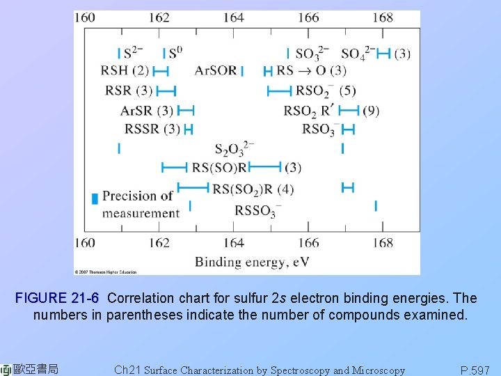
FIGURE 21 -6 Correlation chart for sulfur 2 s electron binding energies. The numbers in parentheses indicate the number of compounds examined. 歐亞書局 Ch 21 Surface Characterization by Spectroscopy and Microscopy P. 597

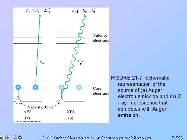
FIGURE 21 -7 Schematic representation of the source of (a) Auger electron emission and (b) X -ray fluorescence that competes with Auger emission. 歐亞書局 Ch 21 Surface Characterization by Spectroscopy and Microscopy P. 598

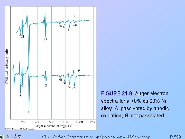
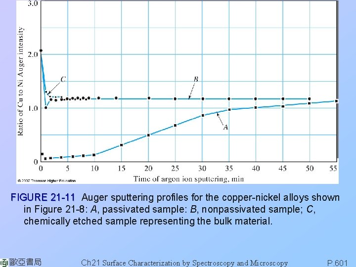
FIGURE 21 -8 Auger electron spectra for a 70% cu: 30% Ni alloy. A, passivated by anodic oxidation; B, not passivated. 歐亞書局 Ch 21 Surface Characterization by Spectroscopy and Microscopy P. 599

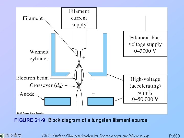
FIGURE 21 -9 Block diagram of a tungsten filament source. 歐亞書局 Ch 21 Surface Characterization by Spectroscopy and Microscopy P. 600

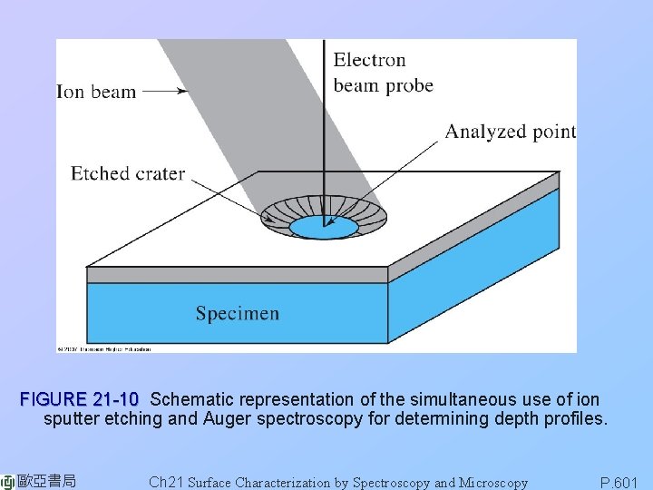
FIGURE 21 -10 Schematic representation of the simultaneous use of ion sputter etching and Auger spectroscopy for determining depth profiles. 歐亞書局 Ch 21 Surface Characterization by Spectroscopy and Microscopy P. 601

FIGURE 21 -11 Auger sputtering profiles for the copper-nickel alloys shown in Figure 21 -8: A, passivated sample: B, nonpassivated sample; C, chemically etched sample representing the bulk material. 歐亞書局 Ch 21 Surface Characterization by Spectroscopy and Microscopy P. 601

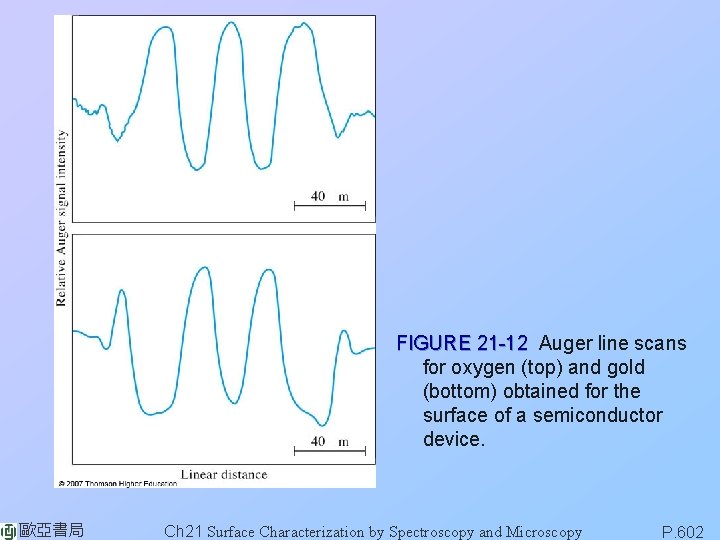
FIGURE 21 -12 Auger line scans for oxygen (top) and gold (bottom) obtained for the surface of a semiconductor device. 歐亞書局 Ch 21 Surface Characterization by Spectroscopy and Microscopy P. 602

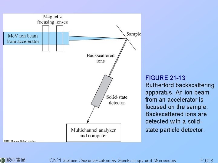
FIGURE 21 -13 Rutherford backscattering apparatus. An ion beam from an accelerator is focused on the sample. Backscattered ions are detected with a solidstate particle detector. 歐亞書局 Ch 21 Surface Characterization by Spectroscopy and Microscopy P. 603

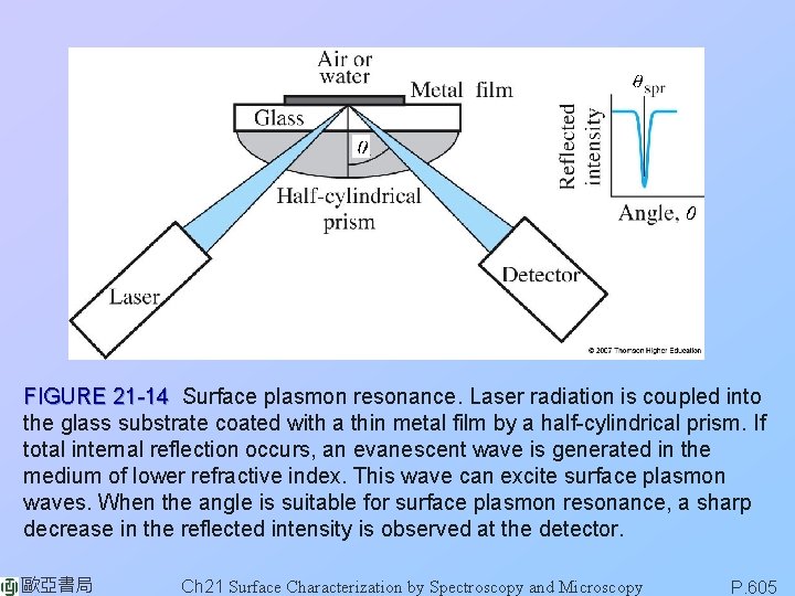
FIGURE 21 -14 Surface plasmon resonance. Laser radiation is coupled into the glass substrate coated with a thin metal film by a half-cylindrical prism. If total internal reflection occurs, an evanescent wave is generated in the medium of lower refractive index. This wave can excite surface plasmon waves. When the angle is suitable for surface plasmon resonance, a sharp decrease in the reflected intensity is observed at the detector. 歐亞書局 Ch 21 Surface Characterization by Spectroscopy and Microscopy P. 605

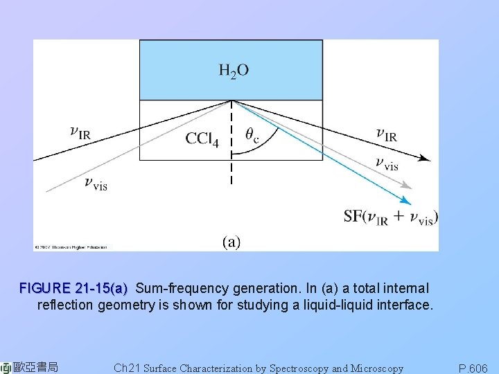
FIGURE 21 -15(a) Sum-frequency generation. In (a) a total internal reflection geometry is shown for studying a liquid-liquid interface. 歐亞書局 Ch 21 Surface Characterization by Spectroscopy and Microscopy P. 606

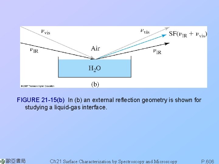
FIGURE 21 -15(b) In (b) an external reflection geometry is shown for studying a liquid-gas interface. 歐亞書局 Ch 21 Surface Characterization by Spectroscopy and Microscopy P. 606

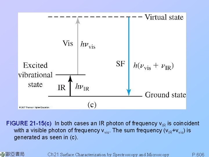
FIGURE 21 -15(c) In both cases an IR photon of frequency νIR is coincident with a visible photon of frequency νvis. The sum frequency (νIR+νvis) is generated as seen in (c). 歐亞書局 Ch 21 Surface Characterization by Spectroscopy and Microscopy P. 606

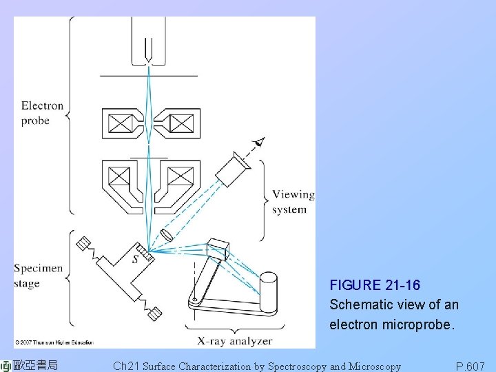
FIGURE 21 -16 Schematic view of an electron microprobe. 歐亞書局 Ch 21 Surface Characterization by Spectroscopy and Microscopy P. 607

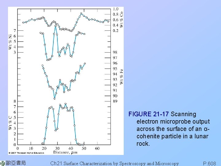
FIGURE 21 -17 Scanning electron microprobe output across the surface of an αcohenite particle in a lunar rock. 歐亞書局 Ch 21 Surface Characterization by Spectroscopy and Microscopy P. 608

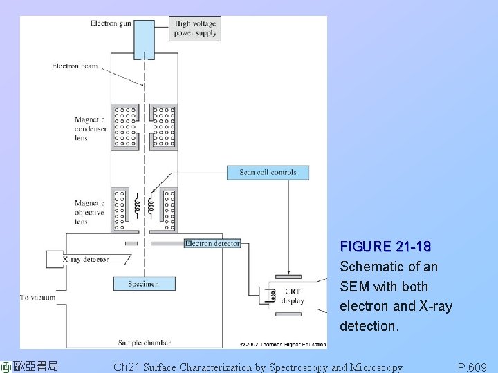
FIGURE 21 -18 Schematic of an SEM with both electron and X-ray detection. 歐亞書局 Ch 21 Surface Characterization by Spectroscopy and Microscopy P. 609

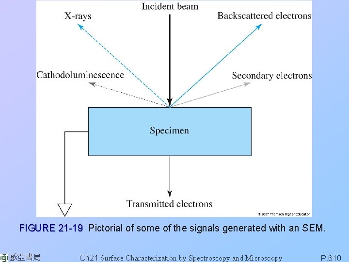
FIGURE 21 -19 Pictorial of some of the signals generated with an SEM. 歐亞書局 Ch 21 Surface Characterization by Spectroscopy and Microscopy P. 610

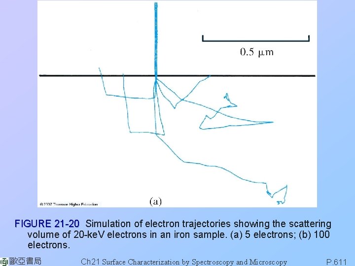
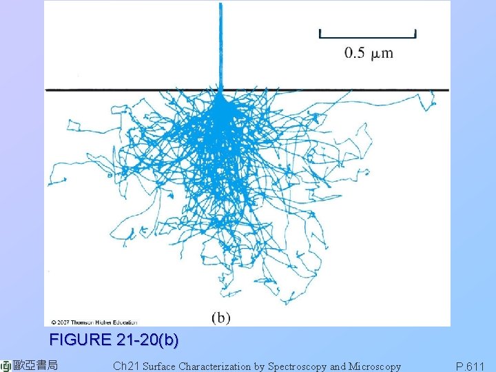
FIGURE 21 -20 Simulation of electron trajectories showing the scattering volume of 20 -ke. V electrons in an iron sample. (a) 5 electrons; (b) 100 electrons. 歐亞書局 Ch 21 Surface Characterization by Spectroscopy and Microscopy P. 611

FIGURE 21 -20(b) 歐亞書局 Ch 21 Surface Characterization by Spectroscopy and Microscopy P. 611

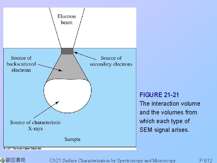
FIGURE 21 -21 The interaction volume and the volumes from which each type of SEM signal arises. 歐亞書局 Ch 21 Surface Characterization by Spectroscopy and Microscopy P. 612

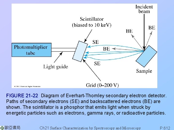
FIGURE 21 -22 Diagram of Everhart-Thornley secondary electron detector. Paths of secondary electrons (SE) and backscattered electrons (BE) are shown. The scintillator is a phosphor that emits light when struck by energetic particles such as electrons, gamma rays, or radioactive particles. 歐亞書局 Ch 21 Surface Characterization by Spectroscopy and Microscopy P. 612

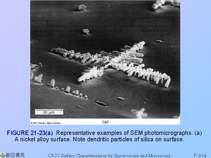
FIGURE 21 -23(a) Representative examples of SEM photomicrographs. (a) A nickel alloy surface. Note dendritic particles of silica on surface. 歐亞書局 Ch 21 Surface Characterization by Spectroscopy and Microscopy P. 614

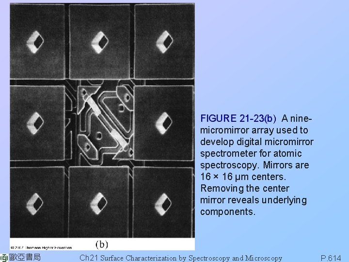
FIGURE 21 -23(b) A ninemicromirror array used to develop digital micromirror spectrometer for atomic spectroscopy. Mirrors are 16 × 16 μm centers. Removing the center mirror reveals underlying components. 歐亞書局 Ch 21 Surface Characterization by Spectroscopy and Microscopy P. 614

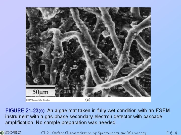
FIGURE 21 -23(c) An algae mat taken in fully wet condition with an ESEM instrument with a gas-phase secondary-electron detector with cascade amplification. No sample preparation was needed. 歐亞書局 Ch 21 Surface Characterization by Spectroscopy and Microscopy P. 614

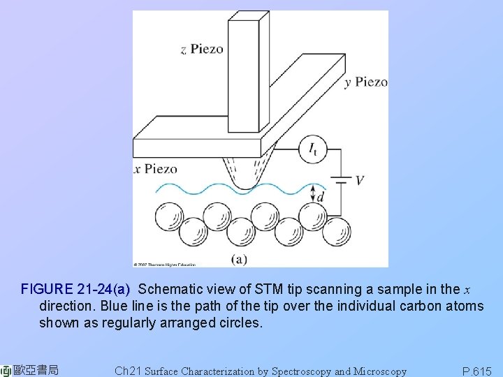
FIGURE 21 -24(a) Schematic view of STM tip scanning a sample in the x direction. Blue line is the path of the tip over the individual carbon atoms shown as regularly arranged circles. 歐亞書局 Ch 21 Surface Characterization by Spectroscopy and Microscopy P. 615

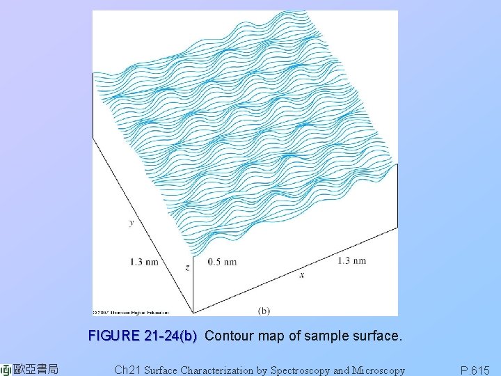
FIGURE 21 -24(b) Contour map of sample surface. 歐亞書局 Ch 21 Surface Characterization by Spectroscopy and Microscopy P. 615

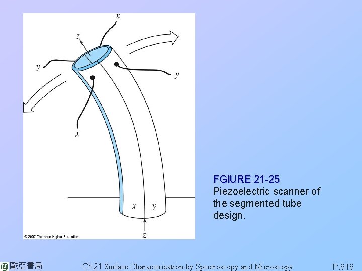
FGIURE 21 -25 Piezoelectric scanner of the segmented tube design. 歐亞書局 Ch 21 Surface Characterization by Spectroscopy and Microscopy P. 616

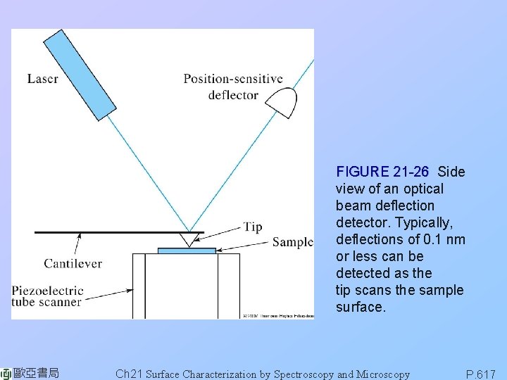
FIGURE 21 -26 Side view of an optical beam deflection detector. Typically, deflections of 0. 1 nm or less can be detected as the tip scans the sample surface. 歐亞書局 Ch 21 Surface Characterization by Spectroscopy and Microscopy P. 617

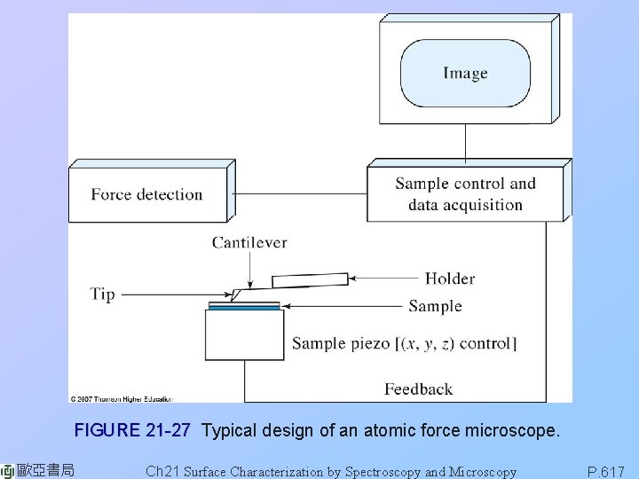
FIGURE 21 -27 Typical design of an atomic force microscope. 歐亞書局 Ch 21 Surface Characterization by Spectroscopy and Microscopy P. 617

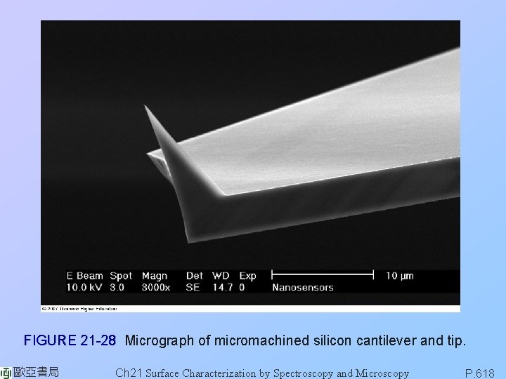
FIGURE 21 -28 Micrograph of micromachined silicon cantilever and tip. 歐亞書局 Ch 21 Surface Characterization by Spectroscopy and Microscopy P. 618

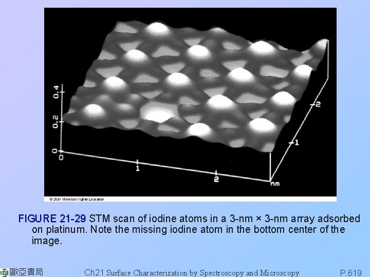
FIGURE 21 -29 STM scan of iodine atoms in a 3 -nm × 3 -nm array adsorbed on platinum. Note the missing iodine atom in the bottom center of the image. 歐亞書局 Ch 21 Surface Characterization by Spectroscopy and Microscopy P. 619

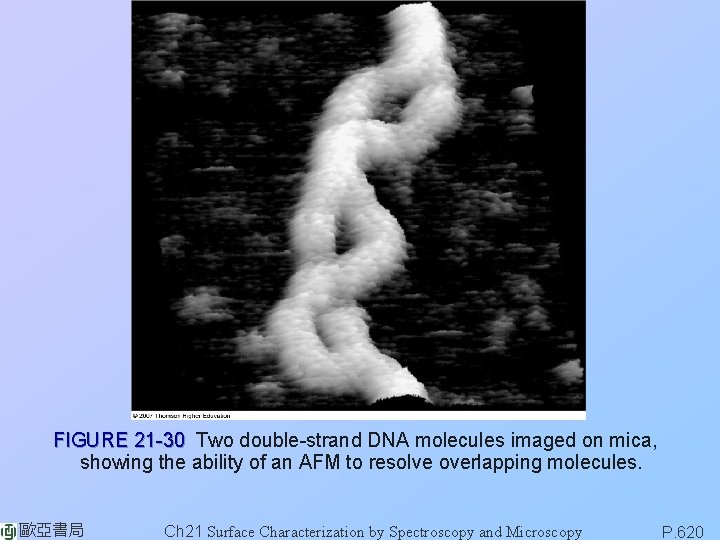
FIGURE 21 -30 Two double-strand DNA molecules imaged on mica, showing the ability of an AFM to resolve overlapping molecules. 歐亞書局 Ch 21 Surface Characterization by Spectroscopy and Microscopy P. 620

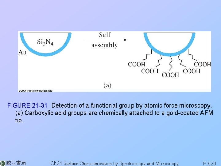
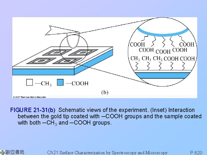
FIGURE 21 -31 Detection of a functional group by atomic force microscopy. (a) Carboxylic acid groups are chemically attached to a gold-coated AFM tip. 歐亞書局 Ch 21 Surface Characterization by Spectroscopy and Microscopy P. 620

FIGURE 21 -31(b) Schematic views of the experiment. (Inset) Interaction between the gold tip coated with ─COOH groups and the sample coated with both ─CH 3 and ─COOH groups. 歐亞書局 Ch 21 Surface Characterization by Spectroscopy and Microscopy P. 620

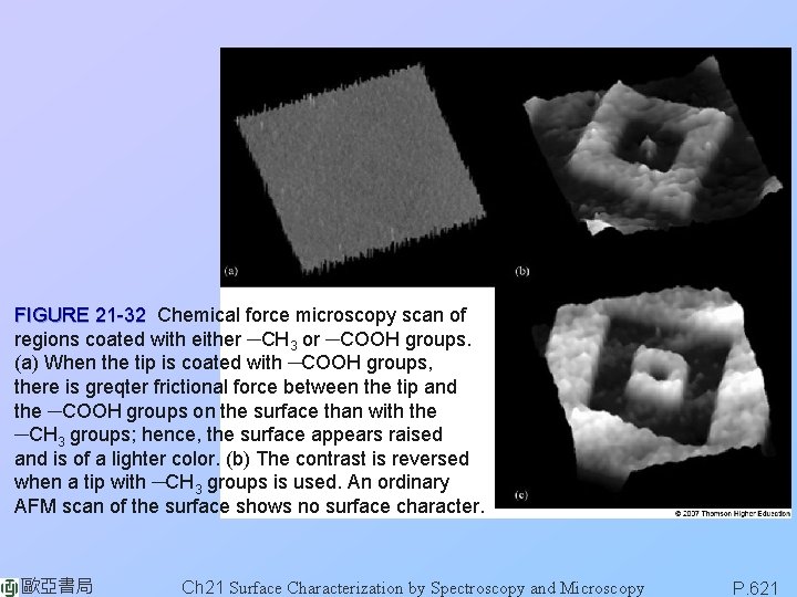
FIGURE 21 -32 Chemical force microscopy scan of regions coated with either ─CH 3 or ─COOH groups. (a) When the tip is coated with ─COOH groups, there is greqter frictional force between the tip and the ─COOH groups on the surface than with the ─CH 3 groups; hence, the surface appears raised and is of a lighter color. (b) The contrast is reversed when a tip with ─CH 3 groups is used. An ordinary AFM scan of the surface shows no surface character. 歐亞書局 Ch 21 Surface Characterization by Spectroscopy and Microscopy P. 621

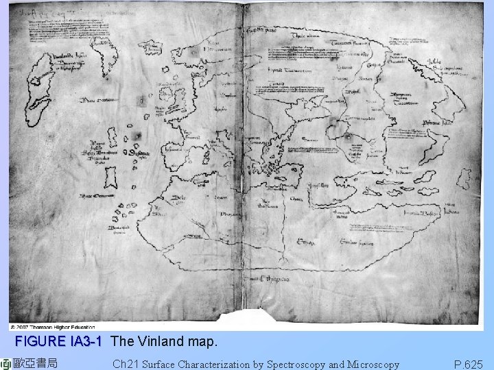
FIGURE IA 3 -1 The Vinland map. 歐亞書局 Ch 21 Surface Characterization by Spectroscopy and Microscopy P. 625