Principle of Microcomputer Based on ARM Technology 19

Principle of Microcomputer Based on ARM Technology (19) 主讲人:陈桂友
CONTENTS • Objectives • STM 32 F 10 x Device • Block Diagram • Memory mapping and boot modes • System Architecture • STM 32 F 10 x System Peripherals • Main features • STM 32 F 10 x Minimum External Components 2 /20
★Objectives: Familiarize with STM 32 F 10 x device Know the main features of the STM 32 F 10 x system peripherals. 3 /20
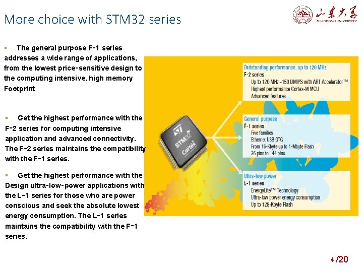
More choice with STM 32 series The general purpose F‑ 1 series addresses a wide range of applications, from the lowest price‑sensitive design to the computing intensive, high memory Footprint Get the highest performance with the F‑ 2 series for computing intensive application and advanced connectivity. The F‑ 2 series maintains the compatibility with the F‑ 1 series. Get the highest performance with the Design ultra‑low‑power applications with the L‑ 1 series for those who are power conscious and seek the absolute lowest energy consumption. The L‑ 1 series maintains the compatibility with the F‑ 1 series. 4 /20
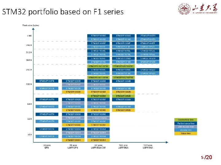
STM 32 portfolio based on F 1 series 5 /20
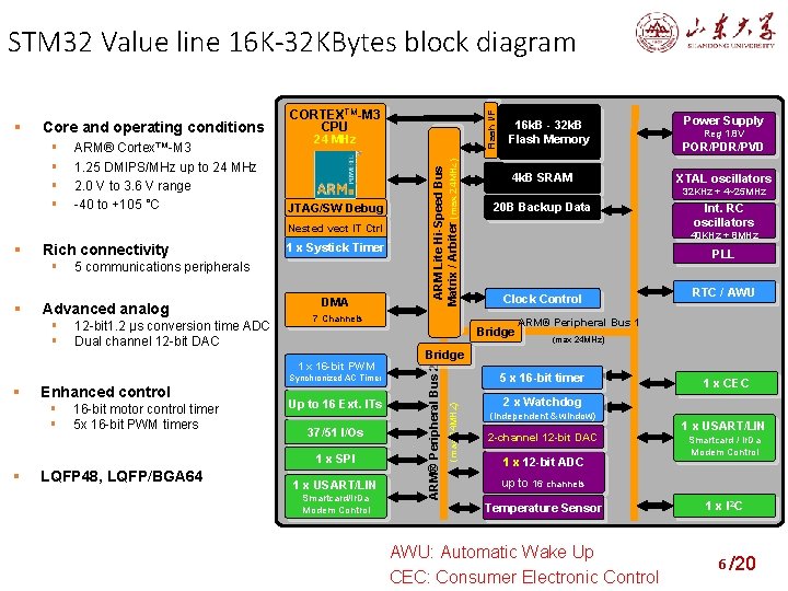
STM 32 Value line 16 K-32 KBytes block diagram 24 MHz JTAG/SW Debug Nested vect IT Ctrl Rich connectivity 1 x Systick Timer 5 communications peripherals Advanced analog 12 -bit 1. 2 µs conversion time ADC Dual channel 12 -bit DAC DMA 16 -bit motor control timer 5 x 16 -bit PWM timers Up to 16 Ext. ITs 37/51 I/Os 1 x SPI LQFP 48, LQFP/BGA 64 4 k. B SRAM 1 x USART/LIN Smartcard/Ir. Da Modem Control Power Supply Reg 1. 8 V POR/PDR/PVD XTAL oscillators 32 KHz + 4~25 MHz 20 B Backup Data Int. RC oscillators 40 KHz + 8 MHz PLL Clock Control Bridge 1 x 16 -bit PWM Enhanced control 16 k. B - 32 k. B Flash Memory 7 Channels Synchronized AC Timer Flash I/F ARM® Cortex™-M 3 1. 25 DMIPS/MHz up to 24 MHz 2. 0 V to 3. 6 V range -40 to +105 °C RTC / AWU ARM® Peripheral Bus 1 (max 24 MHz) Bridge 5 x 16 -bit timer (max 24 MHz) ARM Lite Hi-Speed Bus Matrix / Arbiter (max 24 MHz) Core and operating conditions ARM® Peripheral Bus 2 CORTEXTM-M 3 CPU 1 x CEC 2 x Watchdog (independent & window) 2 -channel 12 -bit DAC 1 x 12 -bit ADC 1 x USART/LIN Smartcard / Ir. Da Modem Control up to 16 channels Temperature Sensor AWU: Automatic Wake Up CEC: Consumer Electronic Control 1 x I 2 C 6 /20
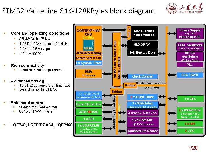
ARM® Cortex™-M 3 1. 25 DMIPS/MHz up to 24 MHz 2. 0 V to 3. 6 V range -40 to +105 °C JTAG/SW Debug Nested vect IT Ctrl Rich connectivity 8 communications peripherals 1 x Systick Timer DMA 7 Channels Advanced analog 12 -bit 1. 2 µs conversion time ADC Dual channel 12 -bit DAC 1 x 16 -bit PWM Synchronized AC Timer Enhanced control 16 -bit motor control timer 6 x 16 -bit PWM timers Up to 16 Ext. ITs 37/51/80 I/Os 1 x SPI LQFP 48, LQFP/BGA 64, LQFP 100 64 k. B - 128 k. B Flash Memory 8 k. B SRAM 1 x USART/LIN Smartcard/Ir. Da Modem Control Power Supply Reg 1. 8 V POR/PDR/PVD XTAL oscillators 32 KHz + 4~25 MHz 20 B Backup Data Int. RC oscillators 40 KHz + 8 MHz PLL Clock Control Bridge RTC / AWU ARM® Peripheral Bus 1 (max 24 MHz) Bridge 6 x 16 -bit Timer (max 24 MHz) 24 MHz ARM® Lite Hi-Speed Bus Matrix / Arbiter (max 24 MHz) Core and operating conditions CORTEXTM-M 3 CPU ARM® Peripheral Bus 2 Flash I/F STM 32 Value line 64 K-128 KBytes block diagram 1 x CEC 2 x Watchdog (independent & window) 2 -channel 12 -bit DAC 2 x USART/LIN Smartcard / Ir. Da Modem Control 1 x 12 -bit ADC up to 16 channels 1 x SPI Temperature Sensor 2 x I 2 C 7 /20
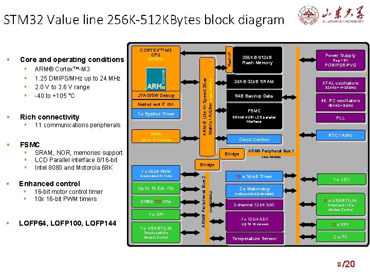
STM 32 Value line 256 K-512 KBytes block diagram JTAG/SW Debug Nested vect IT Ctrl Rich connectivity 11 communications peripherals FSMC 1 x Systick Timer SRAM, NOR, memories support. LCD Parallel interface 8/16 -bit Intel 8080 and Motorola 68 K DMA up to 12 Channels Enhanced control 16 -bit motor control timer 10 x 16 -bit PWM timers LQFP 64, LQFP 100, LQFP 144 24 KB-32 k. B SRAM Power Supply Reg 1. 8 V POR/PDR/PVD XTAL oscillators 32 KHz + 4~25 MHz 84 B Backup Data Int. RC oscillators 40 KHz + 8 MHz FSMC SRAM/ NOR/ LCD parallel interface Clock Control PLL RTC / AWU ARM® Peripheral Bus 1 (max 24 MHz) Bridge 1 x 16 -bit PWM Up to 16 Ext. ITs 51/80/112 I/Os 1 x SPI 256 KB-512 k. B Flash Memory Bridge Synchronized AC Timer Flash I/F ARM® Cortex™-M 3 1. 25 DMIPS/MHz up to 24 MHz 2. 0 V to 3. 6 V range -40 to +105 °C ARM ® Lite Hi-Speed 36 us Matrix / Arbiter (max 24 MHz) 1 x USART/LIN Smartcard/Ir. Da Modem Control 10 x 16 -bit Timer (max 24 MHz) Core and operating conditions ARM® Peripheral Bus 2 CORTEXTM-M 3 CPU 24 MHz 1 x CEC 2 x Watchdog (independent & window) 2 -channel 12 -bit DAC 4 x USART/LIN Smartcard / Ir. Da Modem Control 1 x 12 -bit ADC up to 16 channels 2 x SPI Temperature Sensor 2 x I 2 C 8 /20
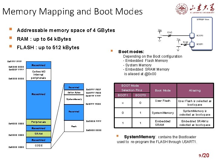
Memory Mapping and Boot Modes Addressable memory space of 4 GBytes RAM : up to 64 k. Bytes FLASH : up to 512 k. Bytes Boot modes: Depending on the Boot configuration - Embedded Flash Memory - System Memory - Embedded SRAM Memory is aliased at @0 x 00 0 x. FFFF 0 x. E 010 0000 0 x. E 00 F FFFF 0 x. E 0000 Reserved Cortex-M 3 internal peripherals Reserved Option Bytes BOOT Mode Selection Pins 0 x 1 FFF F 80 F Reserved 0 x 2000 0000 SRAM Reserved 0 x 0000 User Flash is selected as boot space BOOT 0 0 x 1 FFF F 000 x 0 0 1 System. Memory is selected as boot space 1 1 Embedded SRAM is selected as boot space Reserved 0 x 0801 FFFF Peripherals Aliasing BOOT 1 System. Memory 0 x 4000 0000 Boot Mode 0 x 1 FFF F 800 0 x 1 FFF F 7 FF Flash 0 x 0800 0000 System. Memory: contains the Bootloader used to re-program the FLASH through USART 1. CODE 9 /20
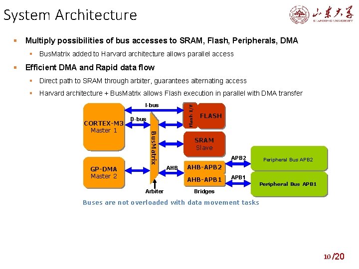
System Architecture Multiply possibilities of bus accesses to SRAM, Flash, Peripherals, DMA Bus. Matrix added to Harvard architecture allows parallel access Efficient DMA and Rapid data flow Direct path to SRAM through arbiter, guarantees alternating access Harvard architecture + Bus. Matrix allows Flash execution in parallel with DMA transfer D-bus Bus. Matrix CORTEX-M 3 Master 1 Flash I/F I-bus GP-DMA Master 2 FLASH SRAM Slave APB 2 AHB-APB 1 Arbiter Peripheral Bus APB 2 AHB-APB 2 APB 1 Peripheral Bus APB 1 Bridges Buses are not overloaded with data movement tasks 10 /20
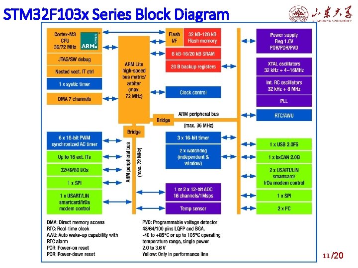
STM 32 F 103 x Series Block Diagram 11 /20
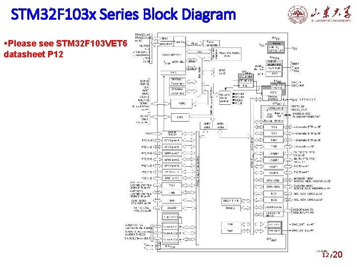
STM 32 F 103 x Series Block Diagram Please see STM 32 F 103 VET 6 datasheet P 12 12 /20
Power Control (PWR) and Backup Domain (BKP) 13 /20
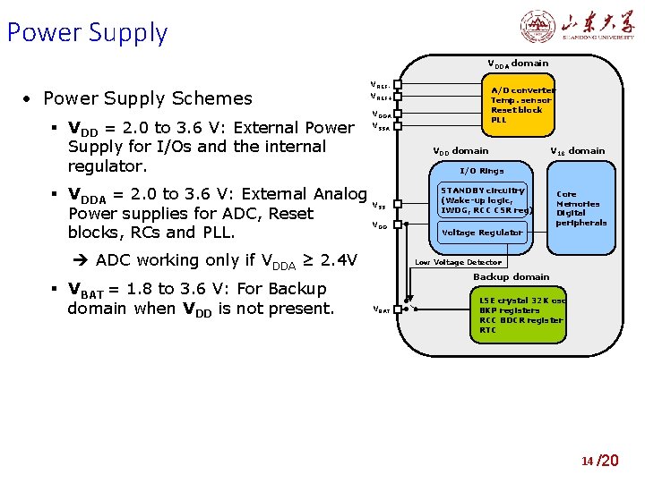
Power Supply VDDA domain • Power Supply Schemes VDD = 2. 0 to 3. 6 V: External Power Supply for I/Os and the internal regulator. VREF+ VDDA VSSA VDD domain V 18 domain I/O Rings VDDA = 2. 0 to 3. 6 V: External Analog V Power supplies for ADC, Reset V blocks, RCs and PLL. SS DD ADC working only if VDDA ≥ 2. 4 V VBAT = 1. 8 to 3. 6 V: For Backup domain when VDD is not present. A/D converter Temp. sensor Reset block PLL STANDBY circuitry (Wake-up logic, IWDG, RCC CSR reg) Voltage Regulator Core Memories Digital peripherals Low Voltage Detector Backup domain VBAT LSE crystal 32 K osc BKP registers RCC BDCR register RTC 14 /20
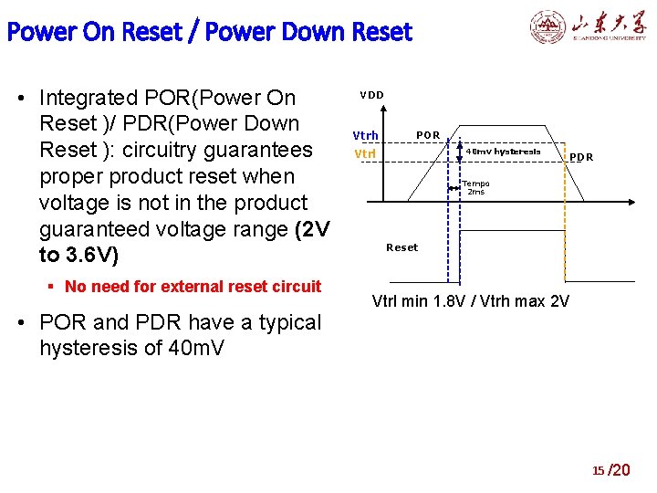
Power On Reset / Power Down Reset • Integrated POR(Power On Reset )/ PDR(Power Down Reset ): circuitry guarantees proper product reset when voltage is not in the product guaranteed voltage range (2 V to 3. 6 V) No need for external reset circuit • POR and PDR have a typical hysteresis of 40 m. V VDD Vtrh POR 40 mv hysteresis Vtrl PDR Tempo 2 ms Reset Vtrl min 1. 8 V / Vtrh max 2 V 15 /20
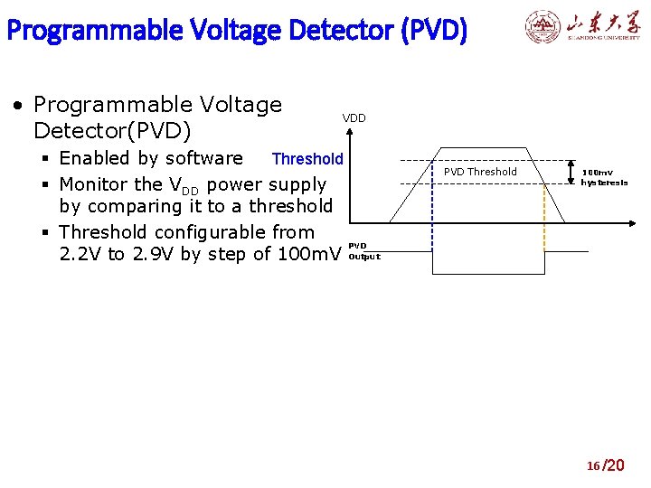
Programmable Voltage Detector (PVD) • Programmable Voltage Detector(PVD) VDD Enabled by software Threshold Monitor the VDD power supply by comparing it to a threshold Threshold configurable from PVD 2. 2 V to 2. 9 V by step of 100 m. V Output PVD Threshold 100 mv hysteresis 16 /20
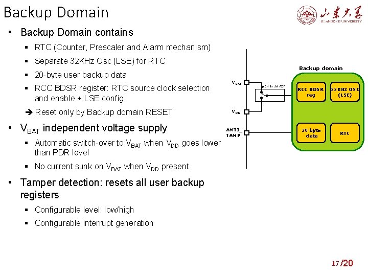
Backup Domain • Backup Domain contains RTC (Counter, Prescaler and Alarm mechanism) Separate 32 KHz Osc (LSE) for RTC 20 -byte user backup data RCC BDSR register: RTC source clock selection and enable + LSE config Reset only by Backup domain RESET • VBAT independent voltage supply Automatic switch-over to VBAT when VDD goes lower than PDR level Backup domain VBAT power switch RCC BDSR reg 32 KHz OSC (LSE) 20 byte data RTC VDD ANTI_ TAMP No current sunk on VBAT when VDD present • Tamper detection: resets all user backup registers Configurable level: low/high Configurable interrupt generation 17 /20
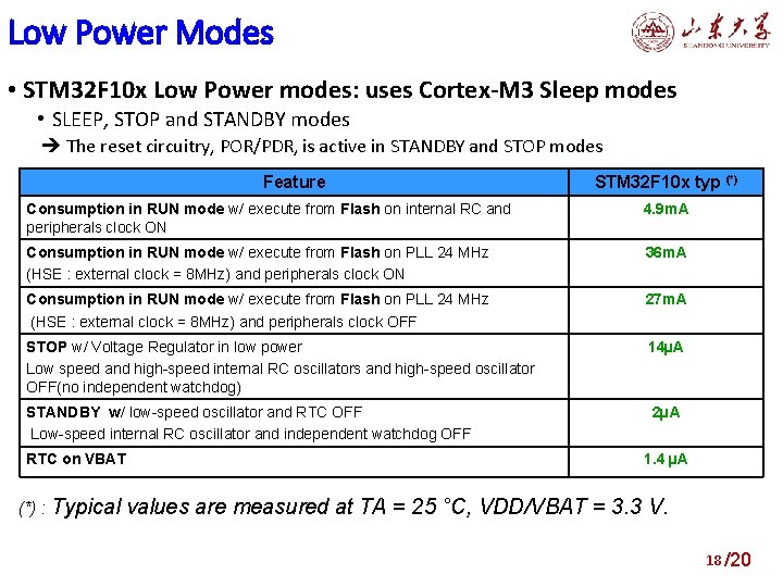
Low Power Modes • STM 32 F 10 x Low Power modes: uses Cortex-M 3 Sleep modes • SLEEP, STOP and STANDBY modes The reset circuitry, POR/PDR, is active in STANDBY and STOP modes Feature STM 32 F 10 x typ (*) Consumption in RUN mode w/ execute from Flash on internal RC and peripherals clock ON 4. 9 m. A Consumption in RUN mode w/ execute from Flash on PLL 24 MHz (HSE : external clock = 8 MHz) and peripherals clock ON 36 m. A Consumption in RUN mode w/ execute from Flash on PLL 24 MHz (HSE : external clock = 8 MHz) and peripherals clock OFF 27 m. A STOP w/ Voltage Regulator in low power Low speed and high-speed internal RC oscillators and high-speed oscillator OFF(no independent watchdog) 14µA STANDBY w/ low-speed oscillator and RTC OFF Low-speed internal RC oscillator and independent watchdog OFF 2µA RTC on VBAT (*) : Typical 1. 4 µA values are measured at TA = 25 °C, VDD/VBAT = 3. 3 V. 18 /20
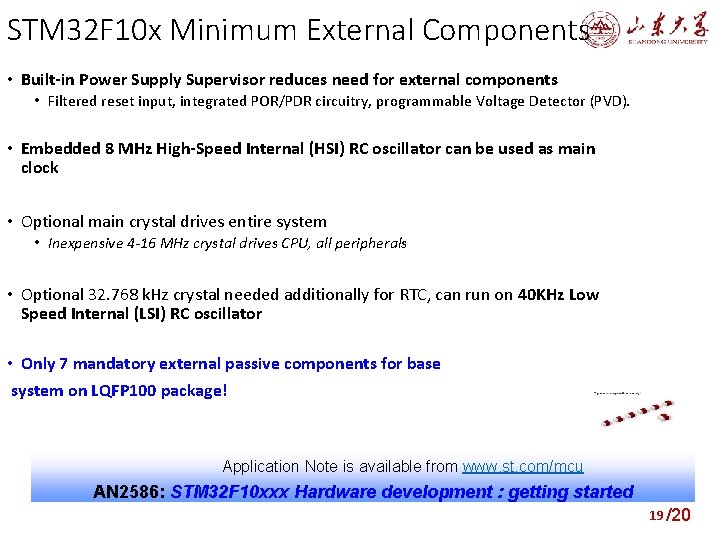
STM 32 F 10 x Minimum External Components • Built-in Power Supply Supervisor reduces need for external components • Filtered reset input, integrated POR/PDR circuitry, programmable Voltage Detector (PVD). • Embedded 8 MHz High-Speed Internal (HSI) RC oscillator can be used as main clock • Optional main crystal drives entire system • Inexpensive 4 -16 MHz crystal drives CPU, all peripherals • Optional 32. 768 k. Hz crystal needed additionally for RTC, can run on 40 KHz Low Speed Internal (LSI) RC oscillator • Only 7 mandatory external passive components for base system on LQFP 100 package! Application Note is available from www. st. com/mcu AN 2586: STM 32 F 10 xxx Hardware development : getting started 19 /20
Next lecture Chapter 4 STM 32 F 10 x Device-2 20 /20
- Slides: 20