PRESENTATION Topic SEM scanning electron microscope University college
 University college of agriculture, University 0 f Sargodha.")


 �EM allows to see those small objects which are not seen")
 �A scanning electron microscope (SEM) is a type of electron")


 tungsten filament (electron source) electrostatic lens (F = q.")

 �When the accelerated primary electrons strikes the sample , it")


 electromagnetic")


 vs Scanning Electron Microscopy (SEM) 25 mm radiolarian OM Small")

- Slides: 25
PRESENTATION Topic SEM (scanning electron microscope) University college of agriculture, University 0 f Sargodha.
BACK-GROUND -STORY �Light microscope was used light source as an illumination. �Visible light which is sensitive to our eyes, so things used visible light are seen under light microscope. (ranges 400700 nm, i. e one nanometer is one billionth of a meter) �This means that we cannot observe things that are much smaller using visible light.
BACK-GROUND -STORY �For example we cannot see cell organelles and atoms using visible light. �Therefore to observe cell organelles and atoms (which are just fractions of a nanometer) we need a microscope that use much smaller wavelength of light waves to see much smaller objects. �For this purpose EM (electron microscope) was invented.
EM (Electron microscope) �EM allows to see those small objects which are not seen by visible light. �It works by using an electron beam instead of visible light and an electron detector instead of our eye. �These electrons behave as a light and have properties of a wave with a wavelength that is much smaller than visible light. �with this smaller wavelength we can distinguish features down to a fraction of a nanometer.
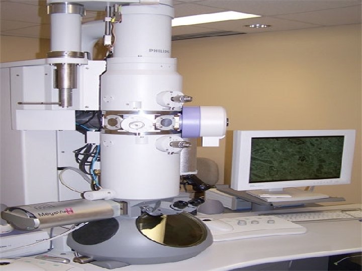
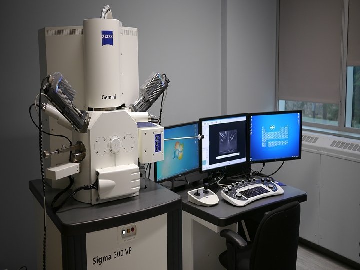
SEM (Scanning electron microscope) �A scanning electron microscope (SEM) is a type of electron microscope that produces images of a sample by scanning the surface with a focused beam of electrons. �The electrons interact with atoms in the sample, producing various signals that contain information about the sample's surface topography and composition. �The electron beam is scanned in a raster scan pattern, and the beam's position is combined with the detected signal to produce an image.
What is SEM? ? Column SEM is designed for direct studying of the surfaces of solid objects Sample Chamber Scanning electron microscope (SEM) is a microscope that uses electrons rather than light to form an image. There are many advantages to using the SEM instead of a OM.
SEM general info
Scanning Electron Microscope (simplified drawing) tungsten filament (electron source) electrostatic lens (F = q. E) accelerating voltage anode e- electromagnetic lenses (F = q v x B) (condenser lenses) electromagnetic lens (objective lens) & deflector coils (raster scan) SE sample detector
HOW THE SEM WORKS? Ø The SEM uses electrons instead of light to form an image. Ø A beam of electrons is produced at the top of the microscope by heating of a metallic filament. Ø The electron beam follows a vertical path through the column of the microscope. It makes its way through electromagnetic lenses which focus and direct the beam down towards the sample. Ø Once it hits the sample, other electrons ( backscattered or secondary ) are ejected from the sample. Detectors collect the secondary or backscattered electrons, and convert them to a signal that is sent to a viewing screen similar to the one in an ordinary television, producing an image.
WORKING PRINCIPLE (simple form) �When the accelerated primary electrons strikes the sample , it produces secondary electrons. these secondary electrons are collected by a positive charged electron detector which in turn gives a 3 - dimensional image of the sample.
How do we get an image? Electron gun 156 electrons! Image
Signals from the sample Incoming electrons Secondary electrons Backscattered electrons X-rays sample
COMPONENTS OF SEM 1. 2. 3. 4. 5. 6. 7. electron gun (filament) electromagnetic optics scan coils sample stage detectors vacuum system computer hardware and software
1. ELECTRON GUN �The electron gun. The electron gun refers to the top region of the SEM that generates a beam of electrons. The simplest and cheapest gun uses a heated tungsten wire to produce electrons
2. ELECTRO-MAGNETIC LENS �A magnetic lens is a device for the focusing or deflection of moving charged particles, such as electrons or ions, by use of the magnetic Lorentz force. Its strength can often be varied by usage of electromagnets. Magnetic lenses are used in diverse applications, from cathode ray tubes over electron microscopy to particle.
3. SCAN COILS �The beam passes through pairs of scanning coils or pairs of deflector plates in the electron column, so that it scans in a raster fashion over a rectangular area of the sample surface.
4. DETECTORS �Detectors. When the electron beam interacts with a sample in a scanning electron microscope (SEM), multiple events happen. In general, different detectors are needed to distinguish secondary electrons, backscattered electrons, or characteristic x-rays.
5. WHY NEED A VACCUME? � When a SEM is used, the electron-optical column and sample chamber must always be at a vacuum. § If the column is in a gas filled environment, electrons will be scattered by gas molecules which would lead to reduction of the beam intensity and stability. � Other gas molecules, which could come from the sample or the microscope itself, could form compounds and condense on the sample. This would lower the contrast and obscure detail in the image.
MAIN APPLICATION �Topography The surface features of an object and its texture (hardness, reflectivity… etc. ) �Morphology The shape and size of the particles making up the object (strength, defects in IC and chips. . . etc. ) �Composition The elements and compounds that the object is composed of and the relative amounts of them (melting point, reactivity, hardness. . . etc. ) �Crystallographic Information How the grains are arranged in the object (conductivity, electrical properties, strength. . . etc. )
COMPARISON OF SEM & TEM SEM �SEM is based on scattered electrons. �SEM focuses on the sample’s surface and its composition. �The sample in SEM not need to cut thinner. �SEM has shorter resolution. � • In SEM, pictures are shown on moniter. �SEM also provides a 3 dimensional image TEM �while TEM is based on transmitted electrons. �whereas TEM provides the details about internal composition. � where as there is a need of cut the sample in thin form. �TEM has higher resolution. �In TEM pictures are shown on fluorescent screen. �while TEM provides a 2 dimensional image.
Probe Source of electrons Light source Condenser Magnetic lenses Specimen Objective Eyepiece Projector Specimen CRT Cathode Ray Tube detector OM TEM SEM Principal features of an optical microscope, a transmission electron microscope and a scanning electron microscope, drawn to emphasize the similarities of overall design.
Optical Microscopy (OM ) vs Scanning Electron Microscopy (SEM) 25 mm radiolarian OM Small depth of field Low resolution SEM Large depth of field High resolution